 | ÐлекÑÑоннÑй компоненÑ: MAX2314 | СкаÑаÑÑ:  PDF PDF  ZIP ZIP |
Äîêóìåíòàöèÿ è îïèñàíèÿ www.docs.chipfind.ru
General Description
The MAX2310/MAX2312/MAX2314/MAX2316 are IF
receivers designed for dual-band, dual-mode, and sin-
gle-mode N-CDMA and W-CDMA cellular phone sys-
tems. The signal path consists of a variable gain
amplifier (VGA) and I/Q demodulator. The devices fea-
ture guaranteed +2.7V operation, a dynamic range of
over 110dB, and high input IP3 (-33dBm at 35dB gain,
1.7dBm at -35dB).
Unlike similar devices, the MAX2310 family of receivers
includes dual oscillators and synthesizers to form a
self-contained IF subsystem. The synthesizer's refer-
ence and RF dividers are fully programmable through a
3-wire serial bus, enabling dual-band system architec-
tures using any common reference and IF frequency.
The differential baseband outputs have enough band-
width to suit both N-CDMA and W-CDMA systems, and
offer saturated output levels of 2.7Vp-p at a low +2.75V
supply voltage. Including the low-noise voltage-con-
trolled oscillator (VCO) and synthesizer, the MAX2310
draws only 26mA from a +2.75V supply in CDMA (dif-
ferential IF) mode.
The MAX2310/MAX2312/MAX2314/MAX2316 are avail-
able in 28-pin QSOP packages.
Applications
Single/Dual/Triple-Mode CDMA Handsets
Globalstar Dual-Mode Handsets
Wireless Data Links
Tetra Direct-Conversion Receivers
Wireless Local Loop (WLL)
Features
o Complete IF Subsystem Includes VCO and
Synthesizer
o Supports Dual-Band, Triple-Mode Operation
o VGA with >110dB Gain Control
o Quadrature Demodulator
o High Output Level (2.7V)
o Programmable Charge-Pump Current
o Supports Any IF Frequency Between 40MHz and
300MHz
o 3-Wire Programmable Interface
o Low Supply Voltage (+2.7V)
MAX2310/MAX2312/MAX2314/MAX2316
CDMA IF VGAs and I/Q Demodulators
with VCO and Synthesizer
________________________________________________________________ Maxim Integrated Products
1
19-1507; Rev 1; 3/03
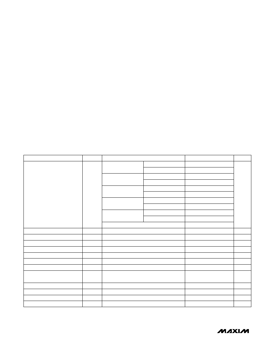
PART
MAX2310EEI
MAX2312EEI
-40°C to +85°C
-40°C to +85°C
TEMP RANGE
PIN-PACKAGE
28 QSOP
28 QSOP
Pin Configurations appear at end of data sheet.
Block Diagram appears at end of data sheet.
Ordering Information
Selector Guide
MAX2314EEI
MAX2316EEI
-40°C to +85°C
-40°C to +85°C
28 QSOP
28 QSOP
Single Band, Dual Mode
AMPS,
Cellular CDMA
MAX2314
Single Band, Single Mode
PCS CDMA
Dual Band, Triple Mode
AMPS,
Cellular CDMA,
PCS CDMA
MAX2310
MAX2312
DESCRIPTION
MODE
PART
Single Band, Single Mode or
Single Band, Dual Mode with
External Discriminator
Cellular CDMA
MAX2316
40MHz to 150MHz
40MHz to 150MHz
67MHz to 300MHz
40MHz to 300MHz
INPUT RANGE
EVALUATION KIT
AVAILABLE
For pricing, delivery, and ordering information, please contact Maxim/Dallas Direct! at
1-888-629-4642, or visit Maxim's website at www.maxim-ic.com.
I
CC
MAX2310/MAX2312/MAX2314/MAX2316
CDMA IF VGAs and I/Q Demodulators
with VCO and Synthesizer
2
_______________________________________________________________________________________
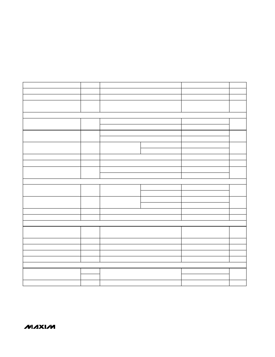
ABSOLUTE MAXIMUM RATINGS
DC ELECTRICAL CHARACTERISTICS
(V
CC
= +2.7V to +5.5V, MODE = DIVSEL = SHDN = STBY = BUFEN = high, differential output load = 10k
, T
A
= -40°C to +85°C,
registers set to default power-up settings. Typical values are at V
CC
= +2.75V and T
A
= +25°C, unless otherwise noted.)
Stresses beyond those listed under "Absolute Maximum Ratings" may cause permanent damage to the device. These are stress ratings only, and functional
operation of the device at these or any other conditions beyond those indicated in the operational sections of the specifications is not implied. Exposure to
absolute maximum rating conditions for extended periods may affect device reliability.
V
CC
to GND ..............................................................-0.3V, +6.0V
SHDN to GND.............................................-0.3V to (V
CC
+ 0.3V)
STBY, BUFEN, MODE, EN, DATA,
CLK, DIVSEL ...........................................-0.3V to (V
CC
+ 0.3V)
VGC to GND...............-0.3V, the lesser of +4.2V or (V
CC
+ 0.3V)
AC Signals TankH ±, TankL ±,
REF, FM ±, CDMA ± .................................................1.0V peak
Digital Input Current SHDN, MODE, DIVSEL,
BUFEN, DATA, CLK, EN, STBY .....................................±10mA
Continuous Power Dissipation (T
A
= +70°C)
28-pin QSOP (derate 10mW/°C above T
A
= +70°C) ....800mW
Operating Temperature Range ...........................-40°C to +85°C
Junction Temperature ......................................................+150°C
Storage Temperature Range .............................-65°C to +160°C
Lead Temperature (soldering, 10s) .................................+300°C
V
CC
= 2.75V
CDMA mode
I+ to I- and Q+ to Q-, PLL locked
50k
load
50k
load
SHDN = low
0.5V < V
VGC
< 2.3V
Addition for LO out (BUFEN = low)
CONDITIONS
V
V
CC
- 1.4
Common-Mode Output Voltage
mV
-20
±1.5
+20
DC Offset Voltage
V
0.5
Lock Indicator Low (unlocked)
V
2.0
Lock Indicator High (locked)
µA
1
VGC Control Input Current
During Shutdown
µA
-5
5
VGC Control Input Current
µA
2
I
IL
Logic Low Input Current
41.5
25.9
37.5
µA
2
I
IH
Logic High Input Current
V
0.5
Logic Low
V
2.0
Logic High
mA
3
5.8
I
CC
Register Shutdown Current
3.5
UNITS
MIN
TYP
MAX
SYMBOL
PARAMETER
T
A
= +25°C
T
A
= -40°C to +85°C
I
CC
Supply Current (Note 1)
mA
T
A
= +25°C
T
A
= -40°C to +85°C
FM IQ mode
40.6
25.4
36.7
T
A
= +25°C
T
A
= -40°C to +85°C
FM I mode
39.5
24.7
35.7
T
A
= +25°C
T
A
= -40°C to +85°C
STANDBY (VCO_H)
20.7
12.3
18.8
T
A
= +25°C
T
A
= -40°C to +85°C
STANDBY (VCO_L)
20.3
11.5
18.4
SHDN = low
µA
1.5
10
I
CC
Shutdown Current
MAX2310/MAX2312/MAX2314/MAX2316
CDMA IF VGAs and I/Q Demodulators
with VCO and Synthesizer
_______________________________________________________________________________________
3
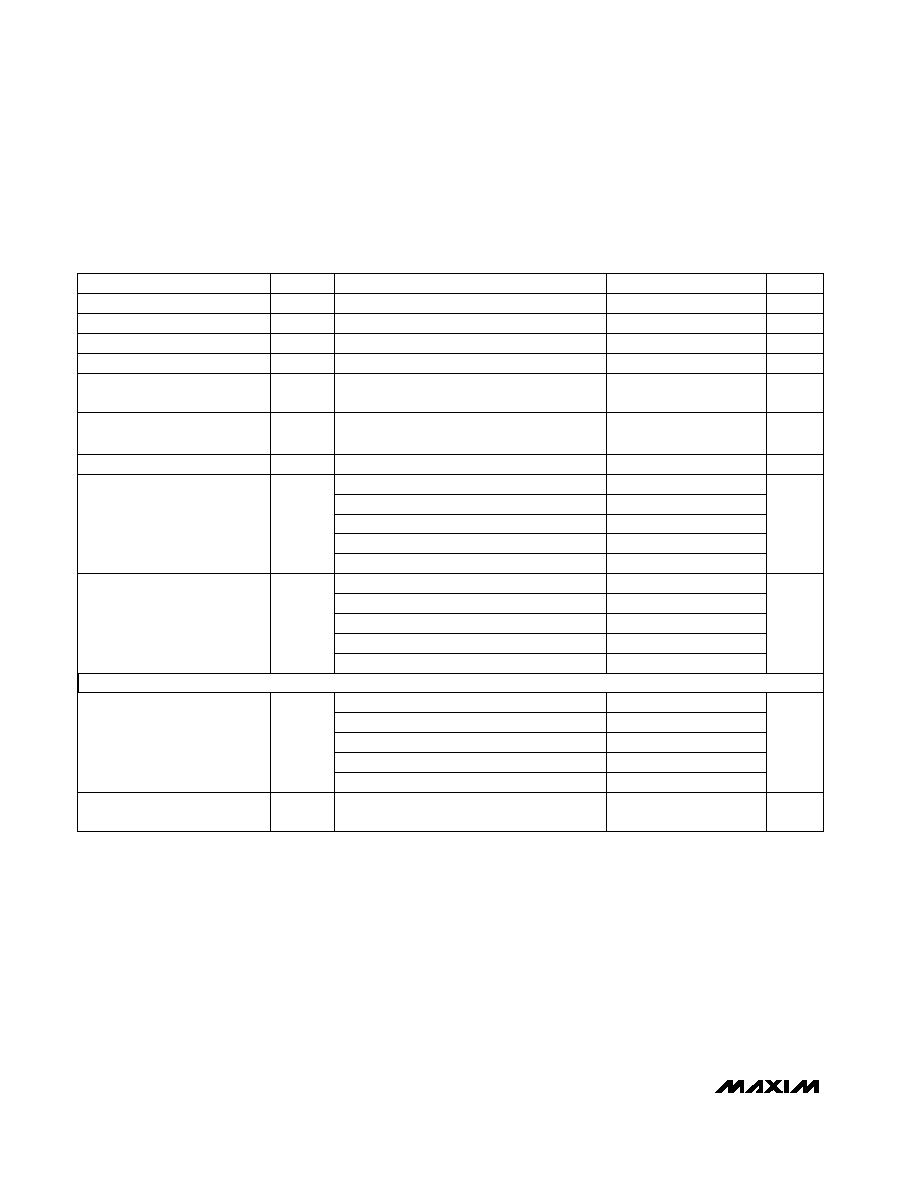
AC ELECTRICAL CHARACTERISTICS
(MAX2310/MAX2314 or MAX2312/MAX2316 EV kit, V
CC
= +2.75V, registers set to default power-up states, f
IN
= 210.88MHz for
CDMA, f
IN
= 85.88MHz for FM, f
REF
= 19.68MHz, synthesizer locked with passive 2nd-order lead-lag loop filter, SHDN = high, VGC
set for +35dB voltage gain, differential output load = 10k
, all power levels referred to 50, T
A
= +25°C, unless otherwise noted.)
(Note 2)
(Note 2)
Gain = +35dB
(Note 5)
Gain = -35dB
Gain = +35dB
Gain = -35dB
Gain = -35dB (Note 3)
Gain = +35dB (Note 4)
CONDITIONS
dBm
-31
IIP3
Input Third-Order Intercept
-6.0
dB
6.36
NF
DSB Noise Figure
62.9
dB
56
61.3
A
V
Maximum Voltage Gain
dB
-54.8
-49
A
V
Minimum Voltage Gain
Vp-p
0.2
V
REF
Frequency Reference Signal
Level
MHz
39
f
REF
MHz
40
300
f
IN
Input Frequency
Reference Frequency
dBm
-49
Input 0.25dB Desensitization
-14.8
dBm
-44
-38.3
P
1dB
Input 1dB Compression
-9
-6.4
1.7
dBm
-33.2
IIP3
Input Third-Order Intercept
UNITS
MIN
TYP
MAX
SYMBOL
PARAMETER
(Notes 6, 8)
dBm
-44
-38.4
P
1dB
Input 1dB Compression
-20
-16.2
dB
58.5
63.4
A
V
Maximum Voltage Gain
dB
-50.2
-47.4
A
V
Minimum Voltage Gain
MHz
4.2
Normalized to +25°C
Baseband 0.5dB Bandwidth
Differential
T
A
= T
MIN
to T
MAX
(Note 6)
Vp-p
2.7
V
SAT
Saturated Output Level
mVp-p
dB
±2.5
Maximum Gain Variation
Over Temperature
1
LO to Baseband Leakage
dB
+28
+35
Quadrature Suppression
R
L
= 50
, BUFEN = low
(Note 2)
dBm
-13.7
P
LO
LOOUT Output Power
MHz
135
600
f
VCO_H
VCO Tune Range
80
300
f
VCO_L
SIGNAL PATH, CDMA MODE
SIGNAL PATH, FM_IQ MODE
SIGNAL PATH, CDMA and FM_IQ MODE
PHASE-LOCKED LOOP
Gain = +35dB
V
GC
= 0.5V (Note 6)
Gain = -35dB
Gain = -35dB
V
GC
= 0.5V (Note 6)
Gain = -35dB
Gain = +35dB
(Note 7)
Gain = +35dB
V
GC
= 2.3V (Note 6)
V
GC
= 2.3V (Note 6)
MAX2310/MAX2312/MAX2314/MAX2316
CDMA IF VGAs and I/Q Demodulators
with VCO and Synthesizer
4
_______________________________________________________________________________________
AC ELECTRICAL CHARACTERISTICS (continued)
(MAX2310/MAX2314 or MAX2312/MAX2316 EV kit, V
CC
= +2.75V, registers set to default power-up states, f
IN
= 210.88MHz for
CDMA, f
IN
= 85.88MHz for FM, f
REF
= 19.68MHz, synthesizer locked with passive 2nd-order lead-lag loop filter, SHDN = high, VGC
set for +35dB voltage gain, differential output load = 10k
, all power levels referred to 50, T
A
= +25°C, unless otherwise noted.)
120kHz offset
30kHz offset
-119
12.5kHz offset
1kHz offset
(Note 6)
(Note 6)
CONDITIONS
-110
30kHz offset
12.5kHz offset
-105
1kHz offset
900kHz offset
-91
-100
-72
dBc
-50
Base Band Spurious due to PLL
-64
dBc/Hz
-125
LOOUT at 85MHz,
VCO_L Enabled (Note 9)
900kHz offset
kHz
1500
Maximum Phase Detector
Comparison Frequency
kHz
20
Minimum Phase Detector
Comparison Frequency
2047
R1, R2
REF Maximum Divide Ratio
2
R1, R2
REF Minimum Divide Ratio
16383
M1, M2
VCO Maximum Divide Ratio
dBc/Hz
-125
256
M1, M2
VCO Minimum Divide Ratio
UNITS
MIN
TYP
MAX
SYMBOL
PARAMETER
120kHz offset
LOOUT at 210MHz,
VCO_H Enabled (Note 9)
Locked, CPX = 00
Acquisition, CPX = XX, TC = 1
105
150
190
-115
1480
2100
2650
Charge-Pump Source/Sink
Current
Note 1:
FM_IQ and FM_I modes are not available on MAX2312 and MAX2316.
Note 2:
Recommended operating frequency range.
Note 3:
f
1
= 210.88MHz, f
2
= 210.89MHz, P
f1
= P
f2
= -15dBm.
Note 4:
f
1
= 210.88MHz, f
2
= 210.89MHz, P
f1
= P
f2
= -50dBm.
Note 5:
Small-signal gain at 200kHz below the LO frequency will be reduced by less than 0.25dB when an interfering signal at
1.25MHz below the LO frequency is applied at the specified level.
Note 6:
Guaranteed by design and characterization.
Note 7:
f
1
= 85.88MHz, f
2
= 85.98MHz, P
f1
= P
f2
= -15dBm.
Note 8:
f
1
= 85.88MHz, f
2
= 85.98MHz, P
f1
= P
f2
= -50dBm.
Note 9:
Measured at LOOUT with BD = 0 (
÷2 selected).
Locked, CPX = 10
Locked, CPX = 01
210
300
380
150
210
265
Locked, all values of CPX,
0.5V < V
CP
< V
CC
- 0.5V
Locked, CPX = 11
%
0.2
10
Charge-Pump Source/Sink
Matching
µA
300
425
530
TURBO LOCK
MAX2310/MAX2312/MAX2314/MAX2316
CDMA IF VGAs and I/Q Demodulators
with VCO and Synthesizer
_______________________________________________________________________________________
5
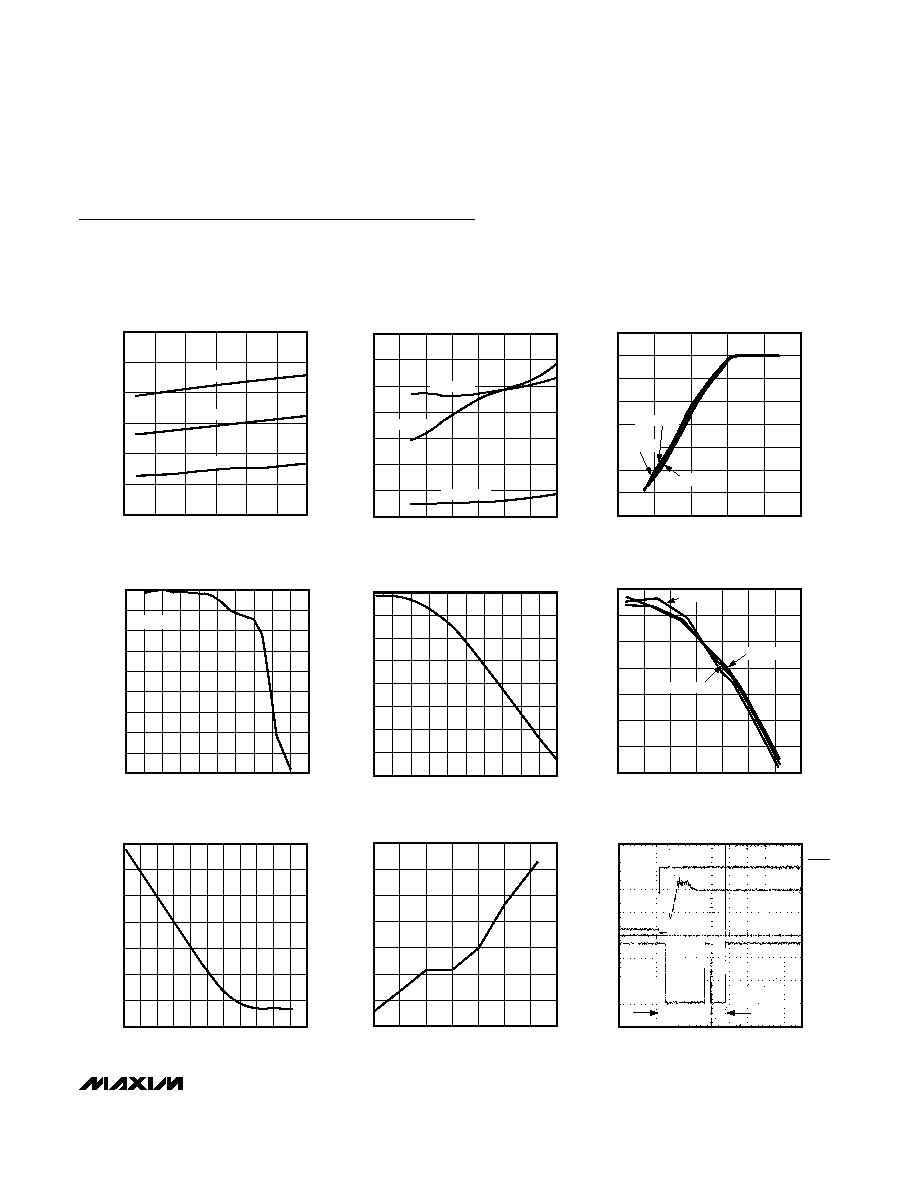
20.00
25.00
22.50
30.00
27.50
32.50
35.00
2.5
3.5
4.0
3.0
4.5
5.0
5.5
RECEIVE SUPPLY CURRENT
vs. SUPPLY VOLTAGE
MAX2310 toc01
SUPPLY VOLTAGE (V)
SUPPLY CURRENT (mA)
T
A
= +85°C
T
A
= +25°C
T
A
= -40°C
0
0.004
0.002
0.008
0.006
0.012
0.010
0.014
2.0
3.0
3.5
2.5
4.0
4.5
5.0
5.5
RECEIVE SHUTDOWN CURRENT vs.
SUPPLY VOLTAGE
MAX2310 toc02
SUPPLY VOLTAGE (V)
SHUTDOWN CURRENT (mA)
T
A
= -40°C
T
A
= +25°C
T
A
= +85°C
-80
-60
-40
-20
0
20
40
60
80
0.5
1.0
1.5
2.0
2.5
3.0
GAIN vs. V
GC
NAX2310 toc03
V
GC
(V)
GAIN (dB)
T
A
= +25°C
T
A
= -40°C
T
A
= +85°C
15
25
20
35
30
40
45
55
50
60
0
100
200
300
400
500
GAIN vs. INPUT FREQUENCY
MAX2310 toc04
FREQUENCY (MHz)
GAIN (dB)
V
GC
= 2.5V
56.0
57.0
56.5
57.5
59.0
59.5
58.5
58.0
60.0
0
4
6
8
10
2
12 14 16 18 20
GAIN vs. BASEBAND FREQUENCY
MAX2310 toc05
FREQUENCY (MHz)
RELATIVE GAIN (dB)
-60
-40
-50
-20
-30
0
-10
10
-60
-20
0
-40
20
40
60
80
THIRD-ORDER INPUT
INTERCEPT vs. GAIN
MAX2310 toc06
GAIN (dB)
IIP3 (dBm)
T
A
= -40°C
T
A
= +85°C
T
A
= +25°C
0
60
20
10
30
40
50
70
-40
-20 -10 0
-30
10 20
50
40
60
30
70
NOISE FIGURE vs. GAIN
MAX2310 toc07
GAIN (dB)
NF (dB)
6.0
6.4
6.2
6.8
6.6
7.2
7.0
7.4
-40
0
20
-20
40
60
80
100
NOISE FIGURE vs. TEMPERATURE
MAX2310 toc08
TEMPERATURE (°C)
NF (dB)
LOCK
VCO
VOLTAGE
VCO VOLTAGE vs. TIME
MAX2310 toc09
TIME (500
µs/div)
VOLTS (1V/div)
SHDN
LOCK TIME
1.83ms
Typical Operating Characteristics
(MAX2310/MAX2314 or MAX2312/MAX2316 EV kit, V
CC
= +2.75V, registers set to default power-up states, f
IN
= 210.88MHz for
CDMA, f
IN
= 85.88MHz for FM, f
REF
= 19.68MHz, synthesizer locked with passive 2nd-order lead-lag loop filter, SHDN = high, VGC
set for +35dB voltage gain, differential output load = 10k
, all power levels referred to 50, T
A
= +25°C, unless otherwise noted.)