 | –≠–ª–µ–∫—Ç—Ä–æ–Ω–Ω—ã–π –∫–æ–º–ø–æ–Ω–µ–Ω—Ç: MAX2338 | –°–∫–∞—á–∞—Ç—å:  PDF PDF  ZIP ZIP |
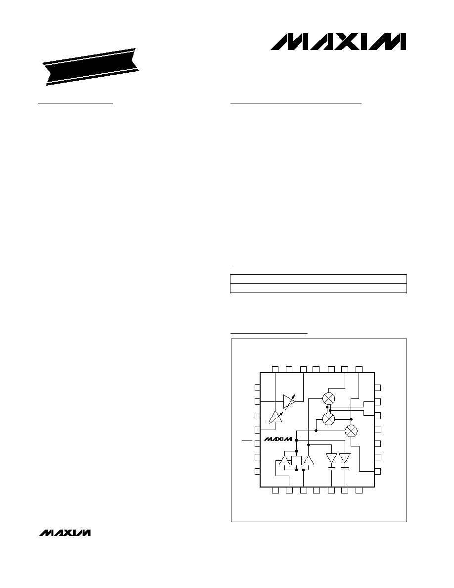
General Description
The MAX2338 receiver RF front-end IC is designed for
dual-band CDMA cellular phones and can also be used
in dual-band TDMA, GSM, or EDGE cellular phones.
Thanks to the MAX2338's on-chip low-power LO
divider, the cellular VCO module can be eliminated.
The MAX2338 includes a low-noise amplifier (LNA) with
an adjustable high-input third-order intercept point
(IIP3) to minimize intermodulation and cross-modulation
in the presence of large interfering signals. For cellular
band operation, a low-gain LNA is available for higher
cascaded IIP3 at lower current.
The CDMA mixers are designed for high linearity, low
noise, and differential IF outputs. The FM mixer is
designed for lower current and single-ended output.
The MAX2338 triple-mode LNA/mixer includes an on-
chip LO frequency divider to allow the use of a single
VCO for both bands. This device is available in an ultra-
small 28-pin leadless QFN package.
________________________Applications
Dual-Band, Triple-Mode PCS/Cellular Phones
Dual-Mode Cellular Phones
Features
o 1.4dB LNA Noise Figure
o 15dB LNA Gain
o Mixer Noise Figure
7.5dB (CDMA)
8.7dB (AMPS)
o Mixer Gain
14.5dB PCS
13.3dB Cellular
8.8dB AMPS
o LO Frequency Divider, Saves VCO Module
o LO Output Buffers for TX
o Ultra-Small 28-Pin Leadless Package
MAX2338
Triple/Dual-Mode CDMA LNA/Mixers
________________________________________________________________ Maxim Integrated Products
1
MAX2338
25
26
27
28
22
23
24
8
9
10
11
12
13
14
15
16
17
18
19
20
21
1
2
3
4
5
6
7
N.C.
GND
LO/2
LOIN
GND
PLOOUT
CLOOUT
CMIXIN
CLNAOUT
GND
PLNAOUT
GND
GND
PMIXIN
GND
CLNAIN
LIN
GAIN
PLNAIN
RLNA
IF-
GND
BUFFEN
V
CC
FMOUT
IF+
RBIAS
QFN
TOP VIEW
˜2
BAND
19-1807; Rev 1; 3/01
EVALUATION KIT
AVAILABLE
Ordering Information
28 QFN
PIN-PACKAGE
TEMP RANGE
-40∞C to +85∞C
MAX2338EGI
PART
Pin Configuration/
Functional Diagram
Typical Operating Circuit appears at end of data sheet.
For pricing, delivery, and ordering information, please contact Maxim/Dallas Direct! at
1-888-629-4642, or visit Maxim's website at www.maxim-ic.com.

MAX2338
Triple/Dual-Mode CDMA LNA/Mixers
2
_______________________________________________________________________________________
ABSOLUTE MAXIMUM RATINGS
DC ELECTRICAL CHARACTERISTICS
(V
CC
= +2.7V to +3.3V, R
RBIAS
= R
RLNA
= 24k
, BUFFEN = LOW, all RF and IF outputs connected to V
CC
, no RF applied, T
A
= -40∞C
to +85∞C. Typical values are at +3.0V and T
A
= +25∞C, unless otherwise noted. Refer to Operational Modes table for control logic.)
Stresses beyond those listed under "Absolute Maximum Ratings" may cause permanent damage to the device. These are stress ratings only, and functional
operation of the device at these or any other conditions beyond those indicated in the operational sections of the specifications is not implied. Exposure to
absolute maximum rating conditions for extended periods may affect device reliability.
V
CC
to GND..........................................................+0.3V to +4.3V
Digital Input Voltage to GND ......................-0.3V to (V
CC
+ 0.3V)
LNA Input Level...............................................................1V peak
LO, Mixer Input Levels .....................................................+5dBm
Digital Input Current .........................................................±10mA
Continuous Power Dissipation (T
A
= +70∞C)
28-Pin QFN (derate 28.5mW/∞C above T
A
= +70∞C) .........2W
Operating Temperature Range ...........................-40∞C to +85∞C
Junction Temperature ......................................................+150∞C
Storage Temperature Range .............................-65∞C to +150∞C
Lead Temperature (soldering, 10s) ................................ +300∞C
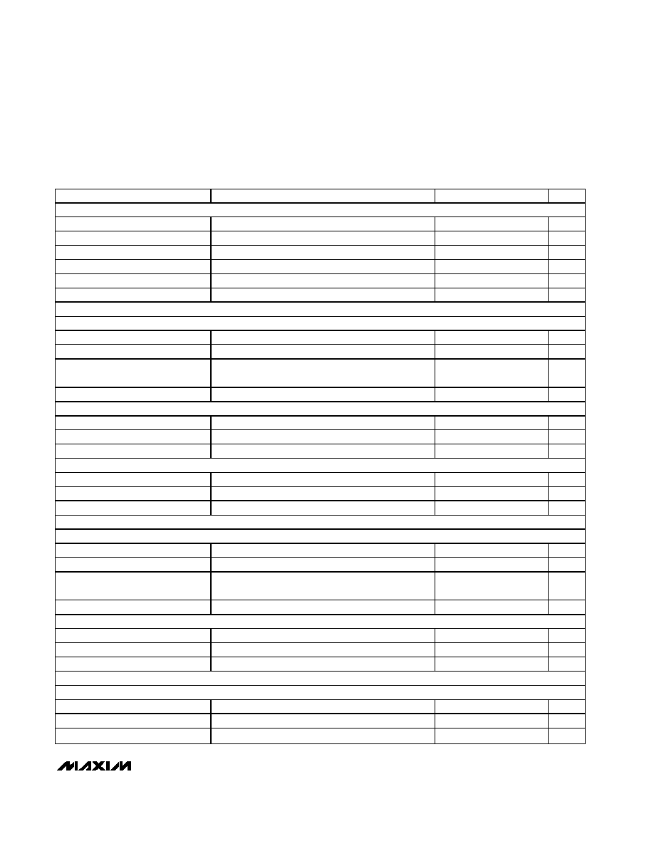
PARAMETER
CONDITIONS
MIN
TYP
MAX
UNITS
PCS CDMA MODES
High-gain, low-linearity mode
18
24
Operating Supply Current
High-gain, high-linearity mode
25
33
mA
CELLULAR CDMA MODE
Low-gain mode
19.5
25
High-gain, low-linearity mode
18
24
Operating Supply Current
High-gain, high-linearity mode
28
35
mA
FM MODE
Operating Supply Current
13.5
17
mA
SHUTDOWN MODE
Shutdown Supply Current
0.1
5
µA
ALL MODES
LO/2 = LOW
7.2
9.5
LO Buffer Supply Current
BUFFEN = HIGH
LO/2 = HIGH
10.3
mA
Additional Operational Current
Divider Active
Cellular and FM mode; LO/2 = HIGH
1.2
mA
Digital Input Logic High
2.0
V
Digital Input Logic Low
0.6
V
Digital Input High Current
5
µA
Digital Input Low Current
-25
µA
MAX2338
Triple/Dual-Mode CDMA LNA/Mixers
_______________________________________________________________________________________
3
AC ELECTRICAL CHARACTERISTICS
(MAX2338 EV kit, V
CC
= +2.7V to +3.3V, f
PLNAIN
= f
PMIXIN
= 1930MHz to 1990MHz, f
CLNAIN
= f
CMIXIN
= 869MHz to 894MHz, f
IF
=
183MHz, high side LO, LO/2 = LOW. All ports matched to 50
, R
RLNA
= R
RBIAS
= 24k
, T
A
= -40∞C to +85∞C. Typical values are at
T
A
= +25∞C, V
CC
= +3.0V, unless otherwise noted.)
PARAMETER
CONDITIONS
MIN
TYP
MAX
UNITS
OVERALL PERFORMANCE
Low-Band RF Frequency Range
869
894
MHz
High-Band RF Frequency Range
1930
1990
MHz
Low-Band LO Frequency Range
After divider if active (Note 1)
950
1100
MHz
High-Band LO Frequency Range
(Note 1)
1750
2210
MHz
IF Frequency Range
(Note 1)
80
220
MHz
LO Input Level
-7
-3
0
dBm
CELLULAR LNA PERFORMANCE
HIGH-GAIN, HIGH-LINEARITY MODES
Gain (Note 2)
14.0
15.7
17.0
dB
Noise Figure (Note 3)
T
A
= +25
∞C
1.4
1.6
dB
Noise Figure Change Due to
Temperature
T
A
= +25
∞C to T
MAX
0.3
dB
IIP3 (Notes 3, 4)
9.5
12
dBm
CDMA HIGH-GAIN, LOW-LINEARITY MODE AND FM MODE
Gain (Note 2)
13
14.7
16.5
dB
Noise Figure (Note 3)
T
A
= +25
∞C
1.4
1.7
dB
IIP3 (Note 3, 4)
2.5
5.5
dBm
CDMA LOW-GAIN MODE
Gain (Note 2)
-4.0
-2.3
0
dBm
Noise Figure (Note 3)
5
6
dB
IIP3 (Notes 3, 4)
15
18
dBm
PCS LNA PERFORMANCE
CDMA HIGH-GAIN, HIGH-LINEARITY MODE
Gain (Note 2)
13.8
15.3
16.9
dB
Noise Figure (Note 3)
T
A
= +25
∞C
1.4
1.7
dB
Noise Figure Change Due to
Temperature
T
A
= +25
∞C to T
MAX
0.3
dB
IIP3 (Notes 3, 5)
5.0
7.7
dBm
CDMA HIGH-GAIN, LOW-LINEARITY MODE
Gain (Note 2)
13.0
14.5
16.5
dB
Noise Figure (Note 3)
T
A
= +25
∞C
1.4
1.7
dB
IIP3 (Notes 3, 5)
2.5
7.5
dBm
CELLULAR MIXER PERFORMANCE
CDMA HIGH-GAIN, HIGH-LINEARITY, AND LOW-GAIN MODES
Gain (Note 2)
10.3
13.3
16.4
dB
Noise Figure (Note 3)
T
A
= +25
∞C
7.8
9.0
dB
IIP3 (Note 4)
3.0
5.5
dBm

MAX2338
Triple/Dual-Mode CDMA LNA/Mixers
4
_______________________________________________________________________________________
PARAMETER
CONDITIONS
MIN
TYP
MAX
UNITS
HIGH-GAIN, LOW-LINEARITY IDLE MODE
Gain (Note 2)
10.1
13
16
dB
Noise Figure (Note 3)
T
A
= +25
∞C
7.3
9.0
dB
IIP3 (Notes 3, 4)
1.4
3.5
dBm
FM MODE
Gain (Note 2)
6.0
8.8
11.1
dB
Noise Figure (Note 3)
T
A
= +25
∞C
8.7
11.0
dB
IIP3 (Note 4)
1.4
3.4
dBm
PCS MIXER PERFORMANCE
CDMA HIGH-GAIN, HIGH-LINEARITY MODE
Gain (Note 2)
11.7
14.5
17
dB
Noise Figure (Note 3)
T
A
= +25
∞C
7.8
9.0
dB
IIP3 (Notes 3, 5)
3.5
7.5
dBm
HIGH-GAIN, LOW-LINEARITY MODE
Gain (Note 2)
11.2
14
16.2
dB
Noise Figure (Note 3)
T
A
= +25
∞C
7.2
9.0
dB
IIP3 (Note 5)
0.5
2.5
dBm
ALL MODES
Mixer Output 1dB Compression
-1
dBm
4 x 5 Suppression (Note 6)
>45
dB
2 x 2 Inp ut Inter cep t P oi nt ( N otes 3, 7)
25
33
dBm
LO Output Level (Note 3)
Into 50
or 100 load, BUFFEN = HIGH
-12
-6
dBm
LO Output Leakage
BUFFEN = LOW
-35
dBm
LO E m i ssi on at P C S LN A Inp ut P or t
-55
dBm
LO Emission at Cellular LNA Input
Port
-55
dBm
LO Output Harmonic Suppression
BUFFEN = HIGH
-15
dBc
PCS band, 80MHz below LO
-161
LO Output Noise Power
BUFFEN = HIGH
C ell ul ar b and , 45M Hz b el ow LO
-161
dBm/Hz
RF Ports Return Loss
All active RF ports including 2-element matching
10
dB
AC ELECTRICAL CHARACTERISTICS (continued)
(MAX2338 EV kit, V
CC
= +2.7V to +3.3V, f
PLNAIN
= f
PMIXIN
= 1930MHz to 1990MHz, f
CLNAIN
= f
CMIXIN
= 869MHz to 894MHz, f
IF
=
183MHz, high side LO, LO/2 = LOW. All ports matched to 50
, R
RLNA
= R
RBIAS
= 24k
, T
A
= -40∞C to +85∞C. Typical values are at
T
A
= +25∞C, V
CC
= +3.0V, unless otherwise noted.)
Note 1: Operation over this frequency range may require the ports to be rematched for the desired operating frequency.
Note 2: MIN guaranteed by production test, MAX guaranteed by design and characterization.
Note 3: Guaranteed by design and device characterization.
Note 4: Two-tone IIP3. Tested at f
RF1
= 880MHz, f
RF2
= 880.9MHz, and power = -25dBm/tone.
Note 5: Two-tone IIP3. Tested at f
RF1
= 1960MHz, f
RF2
= 1961.25MHz, and power = -25dBm/tone.
Note 6: F
LO
= 1064MHZ, f
RF1
= 887.8MHz at -30dBm, f
RF2
= 881MHz at -100dBm. Performance is measured as P
IF
due to
RF1 - P
IF
due to RF2.
Note 7: F
LO
= 2143MHz, f
RF1
= 2051.5MHz at -35dBm, f
RF2
= 1960MHz at -100dBm. Performance is measured as P
IF
due to
RF1 - P
IF
due to RF2.
_______________________________________________________________________________________
5
MAX2338
Triple/Dual-Mode CDMA LNA/Mixers
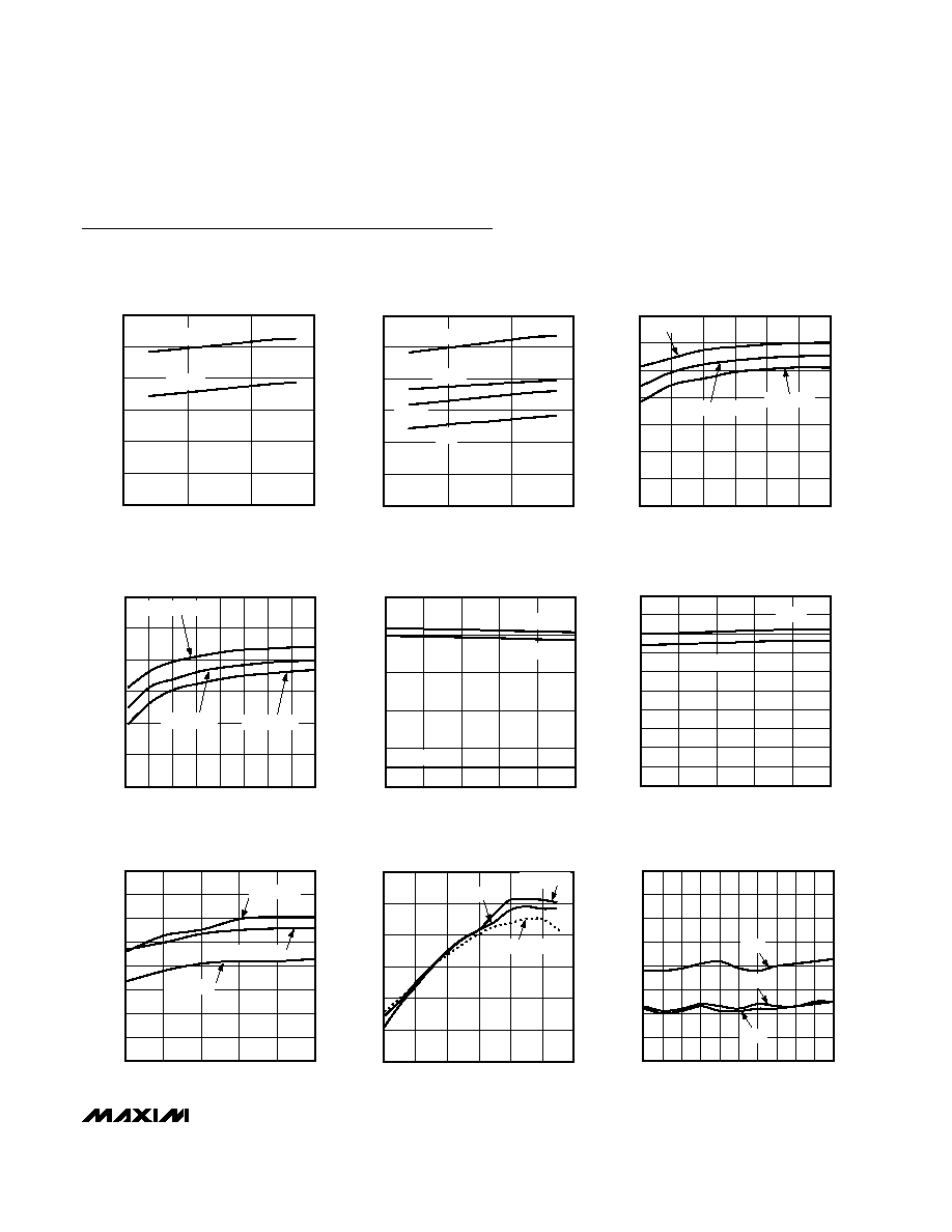
Typical Operating Characteristics
(T
A
= +25∞C, unless otherwise noted.)
0
10
5
20
15
25
30
-50
0
50
100
PCS-BAND SUPPLY CURRENT
MAX2338 toc01
TEMPERATURE (
∞C)
SUPPLY CURRENT (mA)
HGHL
HGLL
-5
0
10
5
15
20
850
870
860
880
890
900
CELLULAR-BAND LNA GAIN
vs. FREQUENCY
MAX2338 toc05
FREQUENCY (MHz)
GAIN (dB)
HGHL
HGLL, FM
LGHL
7
10
9
8
11
12
13
14
15
16
17
1900
1940
1920
1960
1980
2000
PCS-BAND LNA GAIN
vs. FREQUENCY
MAX2338 toc06
FREQUENCY (MHz)
GAIN (dB)
HGHL
HGLL
2
6
4
10
8
12
14
4
8
10
6
12
14
16
CELLULAR-BAND HGHL LNA IIP3
vs. CURRENT
MAX2338 toc08
LNA CURRENT (mA)
IIP3 (dBm)
TA = +85∞C
TA = -40∞C
TA = +25∞C
1.2
1.4
1.3
1.5
1.8
1.9
1.7
1.6
2.0
1900
1920
1940
1960
1980
2000
MAX2338 toc09
FREQUENCY (MHz)
NOISE FIGURE (dB)
PCS-BAND HGHL LNA NOISE FIGURE
vs. FREQUENCY
15mA
8.4mA
4mA
12
17
18
4
8
6
10
12
14
16
18
20
CELLULAR-BAND HGHL LNA GAIN
vs. CURRENT
MAX2338 toc04
LNA CURRENT (mA)
13
GAIN (dB)
14
15
16
TA = -40∞C
TA = +85∞C
TA = +25∞C
2
3
4
5
6
7
8
9
10
4
5
6
7
8
9
PCS-BAND HGHL LNA IIP3
vs. CURRENT
MAX2338 toc07
LNA CURRENT (mA)
IIP3 (dBm)
T
A
= -40
∞C
T
A
= +25
∞C
T
A
= +85
∞C
0
10
5
20
15
25
30
-50
0
50
100
CELLULAR-BAND SUPPLY CURRENT
MAX2338 toc02
TEMPERATURE (
∞C)
SUPPLY CURRENT (mA)
HGHL
LGHL
HGLL
FM
10
12
11
14
13
16
15
17
4
8
10
6
12
14
16
PCS-BAND HGHL LNA GAIN
vs. CURRENT
MAX2338 toc03
LNA CURRENT (mA)
GAIN (dB)
TA = +25∞C
TA = +85∞C
TA = -40∞C