MAX2338 EV KIT
General Description
The MAX2338 evaluation kit (EV kit) simplifies evalua-
tion of the MAX2338 dual-band, triple-mode LNA and
mixers. This kit allows evaluation of the device's low
noise amplifiers (LNA), downconverters and buffers.
Figure 1 shows the MAX2338 EV kit schematic. The EV
kit provides 50
SMA connectors for all RF and IF input
and output signals.
Features
o Easy Evaluation of the MAX2338
o +2.7V to +3.3V Single Supply Operation
o All Critical Matching Components Included
o Cellular-Band RF Ports Matched to 880MHz
o PCS-Band RF Ports Matched to 1960MHz
o SMA Connectors for all RF and IF Signal Ports
o Easy Configuration of Operating Modes
Evaluates: MAX2338
MAX2338 Evaluation Kit
________________________________________________________________ Maxim Integrated Products
1
19-1807; Rev 1; 4/03
PART
MAX2338EVKIT
-40°C to +85°C
TEMP RANGE
IC PACKAGE
28 QFN
Ordering Information
SUPPLIER
PHONE
FAX
AVX
803-946-0690
803-626-3123
EFJohnson
402-474-4800
402-474-4858
WEB
avx-corp.com
efjohnson.com
Component Suppliers
Kamaya
219-489-1533
219-489-2261
kamaya.com
D ESIG N A T IO N QTY
DESCRIPTION
C1, C4, C9
3
0.1µF
±10% ceramic capacitors
(0402)
Murata GRM39X7R103K016A
C2, C3,
C24, C27
6
100pF
±5% ceramic capacitors
(0402)
Murata GRM36COG101J050A
C5, C14, C16
3
6800p F
± 10% cer am i c cap aci tor s
(0402)
Murata GRM36X7R682025A
C6, C13, C15,
C17, C21
3
Not Installed
C7
1
2.7pF
±0.1pF ceramic capacitor
(0402)
Murata GRM36COG2R7B050A
C8
1
0.75pF
±0.1pF ceramic capacitor
(0402)
Murata GRM36COGR75B050A
C10
1
7pF
±0.1pF ceramic capacitor
(0402)
Murata GRM36COG070B050A
C11, C18,
C19, C20,
C26, C28, C33
7
1000p F
± 10% cer am i c cap aci tor s
(0402)
Murata GRM36X7R102050A
C12
1
0
resistor (0402)
Component List
Murata
949-852-2001
949-852-2002
murata.com
Toko
708-297-0070
708-699-1194
toko.com
D ESIG N A T IO N QTY
DESCRIPTION
C22
1
22pF
±5% ceramic capacitor
(0402)
Murata GRM36COG220J050A
C23, C25
2
4.0pF
±0.1pF ceramic capacitors
(0402)
Murata GRM36COG040B050A
C29
1
22µF, 10V m i n tantal um cap aci tor
AVX TAJC226K010
C30
1
15pF
±5% ceramic capacitor
(0603)
Murata GRM39COG150J050A
C31
1
4.7pF
±0.1pF ceramic capacitors
(0402)
Murata GRM36COG4R7B050
R1, R4, R5,
R6, R8
5
1k
±5% resistors (0402)
R2, R3
2
24.3
±1% resistors (0402)
R7
1
3.3k
±1% resistor (0402)
R9, R10
2
0
resistors (0402)
R11
1
8.25k
±5% resistor (0402)
R12, R13
2
Not installed
R14
1
20
±1% resistor (0402)
L1
1
8.2nH inductor
Toko LL1608-FS8N2J
Note: Components in bold text are on the backside of the PC board.
For pricing, delivery, and ordering information, please contact Maxim/Dallas Direct! at
1-888-629-4642, or visit Maxim's website at www.maxim-ic.com.
Note: When contacting these suppliers, please specify that
you are using the MAX2338.
Evaluates: MAX2338
MAX2338 Evaluation Kit
2
_______________________________________________________________________________________
Quick Start
The MAX2338 EV kit is fully assembled and factory test-
ed. Follow the instructions in the Connections and
Setup section for proper device evaluation.
Connections and Setup
This section provides a step-by-step guide to setting up
the MAX2338 EV kit and testing the LNA and downcon-
verters. Do not turn on the DC power or RF signal
generators until all connections are made.
D ESIG N A T IO N
QTY
DESCRIPTION
L2, L12
2
2.7nH inductors
Toko LL1608-FS2N7S
L3
1
0
resistor (0603)
L4
1
2.2nH inductor
Toko LL1608-FS2N2S
L5
1
3.9nH inductor
Toko LL1608-FS2N9J
L6
1
15nH inductor
Toko LL1608-FS15J
L7, L8, L11
3
120nH inductors
Toko LL1608-FS15J
L10
1
Not installed
T1
1
Balun transformer
Toko B5F 458Db-1011
U1
1
MAX2338EGI 44-pin QFN
N O T E: U 1 HA S A N EXPO SED
PA D D L E WH IC H IS SO L D ER ED
T O T H E CIRCUIT BOARD
GROUND PLANE.
D ESIG N A T IO N
QTY
DESCRIPTION
JU2
1
20
±1% resistor (0603)
JU 6, JU 8, JU 10
3
1
2 headers (0.1 inch centers)
JU1, JU3, JU4,
JU5, JU7
5
1
3 headers (0.1 inch centers)
JU1, JU3, JU4,
JU5, JU6, JU7,
JU8, JU10
8
Shunts
PMIXIN,
CMIXIN,
CLOOUT
3
SMA connectors ( PC mount )
Johnson 142-0701-201
CLNAOUT,
IFOUT,
PLNAOUT,
PLNAIN,
CLNAIN, LOIN,
PLOOUT,
FMOUT
8
SMA connectors ( edge mount )
Johnson 142-0701-801
VCC, GND
2
Test points
None
1
MAX2338 data sheet
None
1
MAX2338 EV kit data sheet
None
1
MAX2338 Rev A EV kit circuit
board
Component List (continued)
________________________________________________________ Recommended Test Equipment
Power Supply
Capable of providing at least 100mA at +2.7V to +3.3V.
RF Signal Generators (2)
HP 8648C or equivalent, capable of delivering -50dBm to -10dBm of output power from 800MHz to
2500MHz.
Network Analyzer
HP8753 or equivalent, covering the MAX2338 operating frequency range.
Spectrum Analyzer
HP8561E or equivalent, covering MAX2338 operating frequency range.
Cables (50
)
Three 50
cables with SMA connectors.
Ammeter (optional)
For measuring supply current.
Noise Figure Meter
(optional)
HP8970B or equivalent, for measuring the noise figure of the LNA and downconverters.

Evaluates: MAX2338
MAX2338 Evaluation Kit
_______________________________________________________________________________________
3
Low-Noise Amplifier, High-Gain
High-Linearity Mode
1) Set the GAIN jumper (JU4) on the EV kit to V
CC
(HIGH). This enables the LNA to operate in high
gain mode.
2) Set the BAND jumper (JU1) on the EV kit to V
CC
(HIGH) to test cellular band [JU1 to GND for PCS].
3) Set the LIN jumper (JU3) on the EV kit to V
CC
(HIGH) to test the amplifiers in high linearity mode.
4) Connect a DC supply preset to +3V (through an
ammeter, if desired) to the EV kit's V
CC
and GND
terminals. Do not turn on the supply.
5) Perform a full two-port calibration on a network ana-
lyzer at a power level of -30dBm over frequency
range of 800MHz to 900MHz for cellular band
[1900MHz to 2000MHz for PCS band].
6) Connect port 1 and port 2 of the network analyzer to
CLNAIN [PLNAIN for PCS] and CLNAOUT
[PLNAOUT for PCS] respectively to measure the
cellular [PCS] band gain.
7) Turn on the DC supply. If an ammeter is connected,
the supply current should read approximately 28mA
for cellular band [25mA for PCS].
8) The network analyzer display should indicate a typi-
cal gain of 15.7dB for cellular band and 15.3dB for
PCS band after accounting for board losses. The
input and output board losses are 0.12dB for the
cellular band. The input and output board losses for
PCS band are 0.17dB and 0.3dB, respectively.
These losses are to be added to the measurements
to obtain the performance of the LNAs.
Downconverter
1) Turn off the DC supply.
2) Remove the network analyzer from the LNA input
and output connections. The DC supply connec-
tions needed for testing the downconverter mixer
are the same as in the LNA section.
3) Set the LO/2 jumper (JU5) to V
CC
(ON) to enable
the LO divider circuit for cellular band. When testing
PCS band, this jumper setting has no effect.
4) Set the BAND jumper (JU1) on the EV kit to V
CC
(HIGH) to test cellular band [JU1 to GND for PCS].
5) Set the LIN jumper (JU3) on the EV kit to V
CC
(HIGH) to test cellular and PCS downconverters in
high-linearity mode.
6) Connect an RF signal generator (with output dis-
abled) to the LOIN connector. Set the frequency to
2126MHz for cellular band [2143MHz for PCS] and
the output power to -3dBm.
7) Connect another RF signal generator (with output
disabled) to the CMIXIN SMA connector. Set the
frequency to 880MHz for cellular band [1960MHz
for PCS band] and the output power to -25dBm.
8) Connect the spectrum analyzer to the IFOUT SMA
connector. Set the spectrum analyzer center fre-
quency to 183MHz.
9) Turn on the DC supply. Enable the LO signal gener-
ator and RF input signal generator outputs.
10) Measure the peak of the 183MHz IF signal on the
spectrum analyzer. Compensate the IF signal con-
version gain for the balun and board losses. Balun
loss is 0.3dB and the input and output board losses
are 0.1dB each.
11) The conversion gain for cellular and PCS band are
typically +13.3dB and +14.5dB respectively, after
corrections from step 10 are applied.
Checking Noise Figure
Noise figure measurements are sensitive to board and
lab setup losses and parasitics. There are many tech-
niques and precautions for measuring a low-noise fig-
ure. Detailed explanation of these items goes beyond
the scope of this document. For more information on
how to perform this level of noise figure measurement,
refer to the noise figure meter operating manual, as well
as to Hewlett Packard application note #57-2, Noise
Figure Measurement Accuracy.
PC Board Layout Considerations
The MAX2338 EV kit can serve as a board layout guide.
Keep PC board trace lengths as short as possible to
minimize parasitics. Keep decoupling capacitors close
to the device, with a low inductance connection to the
ground plane.
Evaluates: MAX2338
MAX2338 Evaluation Kit
4
_______________________________________________________________________________________
Figure 1. MAX2338 EV Kit Schematic
MAX2338
U1
CLNAOUT
RLNA
PLNAIN
GND
CLNAIN
LIN
GAIN
RBIAS
IF+
IF-
GND
BUFFEN
V
CC
FM
GND
PLNAOUT
GND
GND
PMIXIN
CMIXIN
GND
LO/2
LOIN
GND
PLOOUT
CLOOUT
N/C
JU2
C2
100pF
L1
8.2nH
L4
2.2nH
C7
2.7pF
R2
24.3k
SMA
CLNAOUT
SMA
PLNAIN
C1
0.01
µ
F
JU10
C3
100pF
L2
2.7nH
C4
0.01
µ
F
V
CC
V
CC
C14
6800pF
SMA
CLNAIN
C16
6800pF
C15
OPEN
L5
3.9nH
C17
OPEN
C11
1000pF
JU1
V
CC
R1
1k
C18
1000pF
C27
100pF
C26
1000pF
C28
1000pF
JU3
V
CC
R4
1k
C19
1000pF
JU4
V
CC
R5
1k
SMA
LOIN
C22
22pF
SMA
PLOOUT
R12
OPEN
SMA
CLOOUT
R13
OPEN
R10
0
R9
0
SMA
FMOUT
JU8
L11
120nH
V
CC
R11
8.25k
R7
3.32k
C33
1000pF
C31
4.7pF
C30
15pF
V
CC
GND
V
CC
JU7
V
CC
R8
1k
JU6
V
CC
L7
120nH
C24
100pF
C23
4.0pF
C25
4.0pF
L8
120nH
3
2
1
4
6
SMA
IFOUT
R3
24.3k
R14
20
L6
15nF
SMA
CMIXIN
L10
OPEN
C10
7pF
C21
OPEN
C9
0.01
µ
F
L3
0
SMA
PMIXIN
L12
2.7nH
C6
OPEN
C5
6800pF
SMA
PLNAOUT
C8
0.75pF
1
2
3
4
5
6
7
8
9
10
11
12
13
14
15
16
17
18
19
20
21
22
23
24
25
26
27
28
C12
0
R6
1k
C20
1000pF
C13
OPEN
JU5
V
CC
C29
22
µ
F
BAND
T1
BALUNTOKO85F
45808-1011
Evaluates: MAX2338
MAX2338 Evaluation Kit
_______________________________________________________________________________________
5
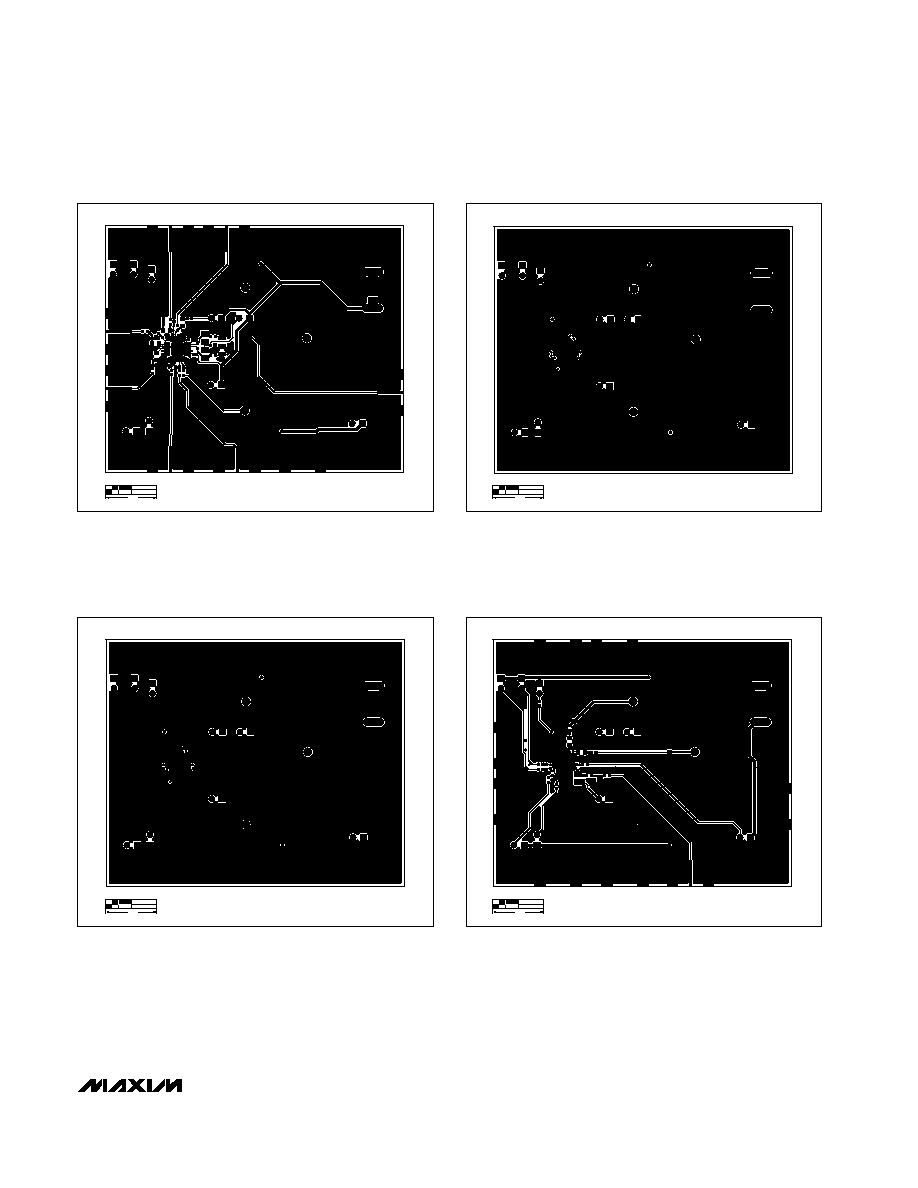
Figure 2. MAX2338 EV Kit PC Board Layout--Front Side
1.0"
Figure 3. MAX2338 EV Kit PC Board Layout--Ground Layer 2
1.0"
Figure 4. MAX2338 EV Kit PC Board Layout--Ground Layer 3
1.0"
Figure 5. MAX2338 EV Kit PC Board Layout--Back Side
1.0"