 | ÐлекÑÑоннÑй компоненÑ: MAX2374 | СкаÑаÑÑ:  PDF PDF  ZIP ZIP |
Äîêóìåíòàöèÿ è îïèñàíèÿ www.docs.chipfind.ru
General Description
The MAX2374 silicon-germanium (SiGe), switchable-
gain, variable-linearity, low-noise amplifier (LNA) is
designed for cellular-band, code-division multiple-
access (CDMA). It can be used for applications such
as TDMA and PDC or wherever high dynamic range
and low noise are required. This LNA provides a high
intermodulation intercept point (IIP3), which is
adjustable to meet specific system requirements by
selecting an appropriate external resistor. To achieve
high gain and low noise, the LNA is packaged in a tiny
ultra-chip-scale package (UCSP) with six solder
bumps. The LNA operates from a +2.7V to +5.5V single
supply and consumes just 8.5mA while achieving a
+6.2dBm input IIP3. Supply current reduces to less
than 1µA in shutdown mode.
The MAX2374 provides two gain modes. High-gain
mode optimizes system sensitivity, while low-gain mode
optimizes system linearity.
Applications
CDMA Phones
TDMA Phones
Wireless Local Loop (WLL)
GSM Handsets
Land Mobile Radio
Wireless Data
Features
o +2.7V to +5.5V Single Supply
o Low Operating Current
8.5mA for High Linearity
4.5mA for Paging
4.1mA in Low-Gain, High-Linearity Mode
o Low Noise Figure: 1.5dB Cellular
o Adjustable IIP3
o Two Gain Settings
o < 1µA Shutdown Mode
o Ultra-Small 6-Bump UCSP (1mm x 1.5mm)
MAX2374
SiGe, Variable IIP3, Low-Noise Amplifier
in UCSP Package
________________________________________________________________ Maxim Integrated Products
1
19-1614; Rev 0; 6/00
EVALUATION KIT MANUAL
FOLLOWS DATA SHEET
Ordering Information
*UCSP reliability is integrally linked to the user's assembly
methods, circuit board material, and environment. Refer to the
UCSP Reliability Notice in the UCSP Reliability section of this
data sheet for more information.
For free samples and the latest literature, visit www.maxim-ic.com or phone 1-800-998-8800.
For small orders, phone 1-800-835-8769.
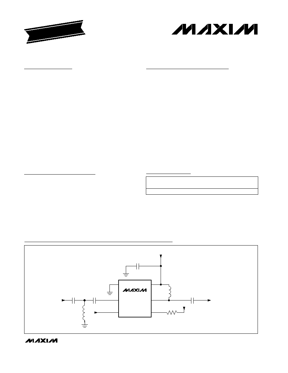
GND
LNAIN
LNA INPUT
LNA OUTPUT
GAIN-CONTROL
LOGIC OUTPUT
A3
B2
B1
B3
A2
A1
LNAOUT
BIAS
R
BIAS
V
CC
V
CC
MAX2374
GAIN
0.01
µF
2pF
100pF
5pF
6.8nH
V
CC
= + 2.75V
8.2nH
Pin Configuration appears at end of data sheet.
Typical Application Circuit
PART
MAX2374EBT
TEMP. RANGE
-40°C to +85°C
PIN-
PACKAGE
6 UCSP*
TOP
MARK
AAB
MAX2374
SiGe, Variable IIP3, Low-Noise Amplifier
in UCSP Package
2
_______________________________________________________________________________________
ABSOLUTE MAXIMUM RATINGS
DC ELECTRICAL CHARACTERISTICS
(V
CC
= +2.7V to +5.5V, R
BIAS
= 20k
, V
GAIN
= high, LNAOUT = V
CC
, no input signals at LNAIN, T
A
= -40°C to +85°C. Typical values
are at V
CC
= +2.75V, T
A
= +25°C, unless otherwise noted.) (Note 1)
Stresses beyond those listed under "Absolute Maximum Ratings" may cause permanent damage to the device. These are stress ratings only, and functional
operation of the device at these or any other conditions beyond those indicated in the operational sections of the specifications is not implied. Exposure to
absolute maximum rating conditions for extended periods may affect device reliability.
V
CC
to GND ...........................................................-0.3V to +6.0V
GAIN, BIAS Voltage to GND...................-0.3V to (V
CC
+ 0.3V)
GAIN, BIAS Current ......................................................±10mA
RF Input Power
LNAIN .........................................................................+10dBm
LNAOUT to GND ....................................-0.3V to (V
CC
+ 0.6V)
Continuous Power Dissipation (T
A
= +85°C) ...................540mW
Operating Temperature Range
MAX2374 .........................................................-40°C to +85°C
Storage Temperature.........................................-65°C to +150°C
Junction Temperature ......................................................+150°C
V
CC
= 2.75V
GAIN = 0.6V, V
CC
= 2.75V
BIAS = open circuit
V
CC
= 5.5V
R
BIAS
= 10k
R
BIAS
= 43k
CONDITIONS
V
V
CC
-
1.16
BIAS Pin Voltage (Note 2)
µA
-5
5
Input Current
V
0.6
Input Logic Voltage Low
V
1.5
Input Logic Voltage High
µA
0.1
1
Shutdown Supply Current
8.5
10.5
V
2.7
5.5
Supply Voltage
mA
4.5
5.5
Supply Current
10.5
15
4.5
UNITS
MIN
TYP
MAX
PARAMETER
AC ELECTRICAL CHARACTERISTICS
(Typical Application Circuit, V
CC
= +2.7V to +5.5V, P
LNAIN
= -30dBm, V
GAIN
= high, f
LNAIN
= 881MHz, R
BIAS
= 20k
, T
A
= +25°C.
Typical values are at V
CC
= +2.75V, unless otherwise noted.) (Note 2)
V
CC
= 2.75V
All modes, f
6.5GHz
Input and output ports externally matched to 50
V
GAIN
= high
CONDITIONS
10:1
Maximum Stable Load VSWR
MHz
750
1000
Recommended Operating Frequency
Range (Note 3)
dBm
-3.5
Output 1dB Compression
dB
14
Input and Output Return Loss
-20
6
UNITS
MIN
TYP
MAX
PARAMETER
V
GAIN
= high
V
GAIN
= low
V
GAIN
= low
dB
-9
Reverse Isolation
SUPPLY
GAIN CONTROL INPUT
T
A
= -40°C to +85°C
MAX2374
SiGe, Variable IIP3, Low-Noise Amplifier
in UCSP Package
_______________________________________________________________________________________
3
AC ELECTRICAL CHARACTERISTICS (continued)
(Typical Application Circuit, V
CC
= +2.7V to +5.5V, P
LNAIN
= -30dBm, V
GAIN
= high, f
LNAIN
= 881MHz, R
BIAS
= 18k
, T
A
= +25°C.
Typical values are at V
CC
= +2.75V, unless otherwise noted.) (Note 2)
V
CC
= 2.75V
CONDITIONS
dB
1.5
1.7
Noise Figure
dB
12.5
17
Gain
13.8
15
15.6
UNITS
MIN
TYP
MAX
PARAMETER
Note 1: Production tested at T
A
= +25°C. Maximum and minimum limits are guaranteed by design and characterization.
Note 2: Guaranteed by design and characterization.
Note 3: Operation over this frequency range is possible with a matching network tuned to the desired operating frequency.
Note 4: Measured with two-tone test with P
LNAIN
= -25dBm per tone, f1 = 881MHz, f2 = 881.9MHz.
0.4
1.2
2
Gain
T
A
= -40°C to +85°C
-1
3.5
dB
Noise Figure
3
3.5
dB
T
A
= +25°C
T
A
= +25°C
T
A
= -40°C to +85°C
7.2
4.5
6.2
MAX2374
dBm
4.2
Input Third-Order Intercept Point (Note 4)
R
BIAS
= 10k
R
BIAS
= 20k
R
BIAS
= 43k
10.5
5.8
7.2
Input Third-Order Intercept Point (Note 4)
MAX2374
1
dBm
HIGH-GAIN MODE (GAIN = V
CC
)
LOW-GAIN MODE (GAIN = GND)
R
BIAS
= 10k
R
BIAS
= 20k
R
BIAS
= 43k
12
10
8
6
4
2.5
4.0
3.0
3.5
4.5
5.0
5.5
I
CC
vs. V
CC
AND TEMPERATURE
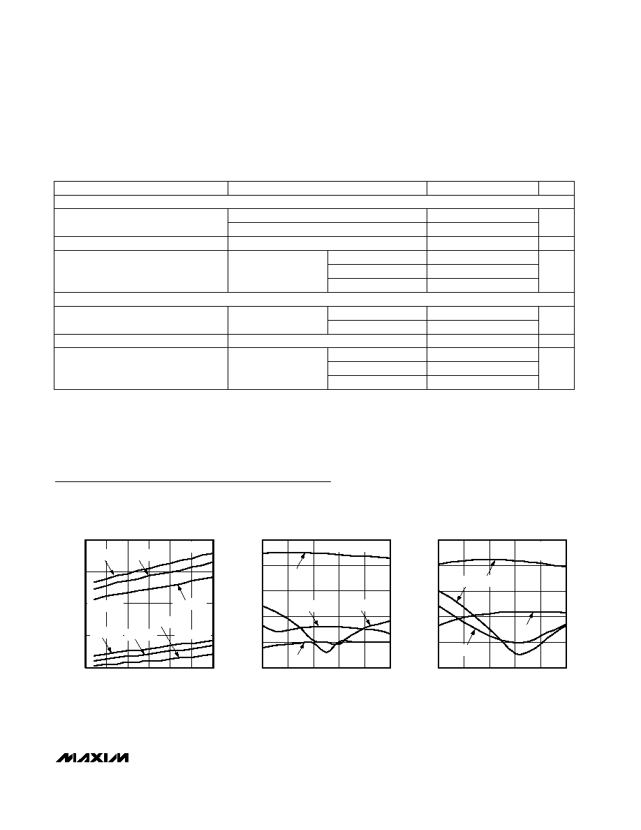
MAX2374-01
V
CC
(V)
I
CC
(mA)
T
A
= -40°C
T
A
= +25°C
T
A
= +85°C
T
A
= +85°C T
A
= +25°C
T
A
= -40°C
GAIN = V
CC
GAIN = GND
R
BIAS
= 20k
-30
-20
0
-10
10
20
750
850
800
900
950
1000
MAX2374-03
FREQUENCY (MHz)
MAGNITUDE (dB)
S21, S11, S22, S12 vs. FREQUENCY
S21
S11
S22
S12
V
CC
= GAIN = 2.75V
-20
-15
-5
-10
0
5
750
850
800
900
950
1000
S21, S11, S22, S12 vs. FREQUENCY
MAX2374-04
FREQUENCY (MHz)
MAGNITUDE (dB)
S21
S12
S11
S22
V
CC
= 2.75V
GAIN = GND
T
A
= -40°C to +85°C
Typical Operating Characteristics
(Typical Application Circuit, V
CC
= +2.7V to +5.5V, P
LNAIN
= -30dBm, f
LNAIN
= 881MHz, R
BIAS
= 20k
, T
A
= +25°C, unless other-
wise noted.)
MAX2374
SiGe, Variable IIP3, Low-Noise Amplifier
in UCSP Package
4
_______________________________________________________________________________________
1.0
2.0
1.5
3.0
2.5
4.0
3.5
4.5
750
850
800
900
950
1000
NOISE FIGURE vs. FREQUENCY
MAX2374-07
FREQUENCY (MHz)
NOISE FIGURE (dB)
V
CC
= 2.75V
GAIN = V
CC
20
15
10
5
0
2.5
4.0
3.0
3.5
4.5
5.0
5.5
CURRENT vs. VOLTAGE AND R
BIAS
MAX2374-08
V
CC
(V)
R
BIAS
= 20k
, GAIN = V
CC
R
BIAS
= 20k
, GAIN = GND
R
BIAS
= 10k
, GAIN = V
CC
R
BIAS
= 10k
, GAIN = GND
R
BIAS
= 43k
, GAIN = GND
R
BIAS
= 43k
, GAIN = V
CC
I
CC
(mA)
Typical Operating Characteristics (continued)
(Typical Application Circuit, V
CC
= +2.7V to +5.5V, P
LNAIN
= -30dBm, f
LNAIN
= 881MHz, R
BIAS
= 20k
, T
A
= +25°C, unless other-
wise noted.)
LNA Output Port. This port requires an external pullup inductor, which may be used as part of the matching
network.
LNAOUT
B2
Supply Voltage Input. Bypass with a 100pF capacitor to GND.
V
CC
B3
LNA Bias Setting Pin. For nominal bias, connect 20k
resistor to V
CC
. Adjust the resistor value to alter the
linearity of the LNA.
BIAS
B1
Gain-Control Logic Input. Drive high for high-gain mode. Drive low for low-gain mode.
GAIN
A1
PIN
LNA Input Port. Blocking capacitor is required, which may be used as part of the matching network.
LNAIN
A2
Ground
GND
A3
FUNCTION
NAME
20
0
5
25
15
35
45
GAIN vs. R
BIAS
AND TEMPERATURE
MAX2374-05
R
BIAS
(k
)
GAIN (dB)
15
10
5
T
A
= +85°C
T
A
= -40°C
T
A
= -40°C
T
A
= +25°C
T
A
= +85°C
T
A
= +25°C
GAIN = V
CC
GAIN = GND
V
CC
= 2.75V
0
20
40
60
IIP3 vs. R
BIAS
AND TEMPERATURE
MAX2374-06
R
BIAS
(k
)
IIP3 (dBm)
0
5
15
10
20
V
CC
= 2.75V,
f = 881MHz, 882MHz
= V
GAIN
= GND
A
= V
GAIN
= V
CC
B
T
A
= +25
°C
T
A
= +85
°C
T
A
= -40
°C
T
A
= +85
°C
A
B
B
T
A
= +25
°C
T
A
= -40
°C
Pin Description
MAX2374
SiGe, Variable IIP3, Low-Noise Amplifier
in UCSP Package
_______________________________________________________________________________________
5
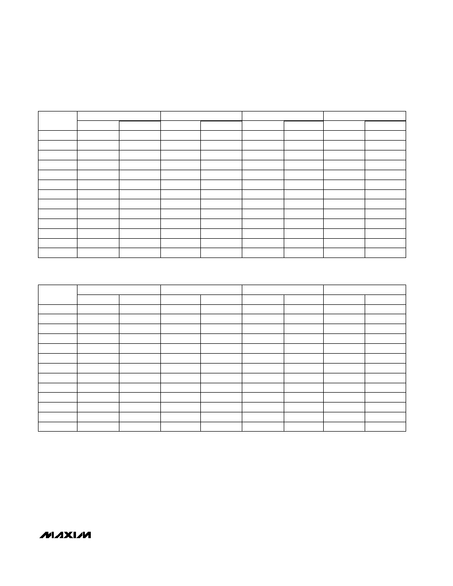
Table 1a. S-Parameters (V
CC
= V
GAIN
= 2.75V)
2250
2500
158.7
146.5
-20.2
78.8
-54.8
S22
0.626
3000
0.689
FREQ (MHz)
0.842
0.908
0.728
2750
250
128
MAGNITUDE
0.68
50
0.671
0.68
0.704
0.732
0.697
-12.9
-45.4
ANGLE
69
123.5
47.6
S12
0.693
500
ANGLE
33.3
21
11.19
5.042
15
17
110
0.686
0.161
0.1
-81
0.026
0.007
-33.3
0.041
-37
0.078
MAGNITUDE
0.053
0.06
0.063
0.057
0.061
0.094
-60.5
750
-77
-105
122.73
-151.3
79.42
S21
0.074
ANGLE
49.35
24.18
1
-19.2
-35
-51
1.01
0.892
-128
9.83
12.84
6.19
-91.7
1000
0.781
MAGNITUDE
4.21
1250
3.12
2.38
1.77
1500
1.46
1.07
149
1750
139
-150
-49
2000
-11.89
-77.5
S11
125
ANGLE
-101
-123.7
-145.2
-165
176
163
0.664
0.691
-171
0.728
0.929
0.571
0.716
162
MAGNITUDE
0.524
0.529
0.568
0.612
0.639
0.652
-104
0.662
111.5
0.72
2250
2500
140
126.35
1.23
85.8
-42
S22
0.534
3000
0.623
FREQ (MHz)
0.471
0.374
0.596
2750
250
103.2
MAGNITUDE
0.659
50
0.689
0.694
0.695
0.681
0.629
-47
-77.2
ANGLE
85.7
127
52.2
S12
0.6
500
ANGLE
19.6
-9.33
-30.7
-47
-53.4
-42.5
85.8
0.566
0.175
0.123
-82
0.06
0.01
-62.8
0.14
-63.3
0.082
MAGNITUDE
0.189
0.2
0.184
0.146
0.117
0.096
-62
750
-89
-117.3
128.8
-148.7
72.4
S21
0.103
ANGLE
28.18
-6.87
-34.5
-54
-66
-66
0.196
0.156
-147.5
1.21
1.25
1
-83
1000
0.096
MAGNITUDE
0.772
1250
0.583
0.429
0.301
1500
0.228
0.148
126.3
1750
112
-173
-42.4
2000
-8.93
-77
S11
92.4
ANGLE
-106
-132.7
-158
180
159.5
141.5
0.739
0.745
164.6
0.916
0.987
0.8
0.701
141.7
MAGNITUDE
0.75
0.754
0.782
0.803
0.811
0.797
-73.48
0.112
73
0.591
Table 1b. S-Parameters (V
CC
= 2.75V, V
GAIN
= GND)