 | –≠–ª–µ–∫—Ç—Ä–æ–Ω–Ω—ã–π –∫–æ–º–ø–æ–Ω–µ–Ω—Ç: MAX2385 | –°–∫–∞—á–∞—Ç—å:  PDF PDF  ZIP ZIP |
General Description
The MAX2385/MAX2386 LNA/mixer ICs are designed
for CDMA/cdma2000 1x and GPS applications. The
MAX2385/MAX2386 are optimized for the Japanese
832MHz to 870MHz band, and can also be configured
for the Korean/Chinese/U.S. 869MHz to 894MHz band.
To optimize linearity and current consumption, the
CDMA LNA comprises four gain states. The high-gain
LNA has a reduced supply-current mode for use when
no transmit (Tx) signal is present, and a high linearity
mode, which minimizes Tx cross-modulation in the
presence of a large interfering signal during talk mode.
Two low-gain modes, provide higher cascade IIP3 at
lower current. The lowest gain setting provides an LNA
bypass and an ultra-low chip current of 4mA. This sig-
nificantly extends the phone's standby time and lowers
the overall current consumption of the phone.
Gain-switching hysteresis can be adjusted by selection
of an off-chip resistor, which sets the current and linear-
ity in each mode to customize switchover points.
In GPS mode, the MAX2386 LNA offers high gain and
the MAX2385 features lower current consumption with
lower gain. The CDMA paths of the MAX2385/MAX2386
are identical.
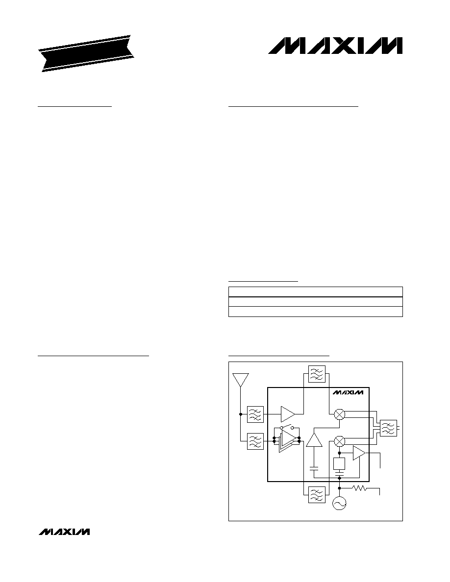
The MAX2385/MAX2386 include an on-chip LO divider,
which enables the use of one VCO module for both cel-
lular and GPS modes. An on-chip LO buffer to drive the
Tx upconverter further reduces system complexity.
Applications
CDMA/cdma2000 1x Cellular Phones with GPS
Features
o Low Average Current Consumption: 4.5mA
(CDMA)
o +2.7V to +3.6V Operation
o 2.0dB Cascade GPS Noise Figure
o 2.5 dB Cascade CDMA Noise Figure
o Adjustable IIP3
o LO Output Buffer to Drive Tx Upconverter
o 1µA Shutdown Current
o Tiny 2.1mm
2.7mm Chip-Scale Package
(UCSPTM)
o Single VCO for GPS and CDMA Operation
o LO Divider Improves Phase Noise/Desensitization
MAX2385/MAX2386
CDMA + GPS LNA/Mixers
________________________________________________________________ Maxim Integrated Products
1
19-2205; Rev 0; 10/01
For pricing, delivery, and ordering information, please contact Maxim/Dallas Direct! at
1-888-629-4642, or visit Maxim's website at www.maxim-ic.com.
*Requires a special solder temperature profile described in the
Absolute Maximum Ratings section.
EVALUATION KIT
AVAILABLE
Ordering Information
PART
TEMP. RANGE
BUMP-PACKAGE
MAX2385EBP-T
-40
∞C to +85∞C
5
4 UCSP*
MAX2386EBP-T
-40
∞C to +85∞C
5
4 UCSP*
UCSP is a trademark of Maxim Products, Inc.
MAX2385
MAX2386
CDMA PATH
VCO
LO BUFFER
ENABLE
LO BUFFER
OUTPUT
GPS PATH
˜2
Block Diagram
Pin Configuration/Functional Diagram/Typical Operating
Circuit appears at end of data sheet.
MAX2385/MAX2386
CDMA + GPS LNA/Mixers
2
_______________________________________________________________________________________
ABSOLUTE MAXIMUM RATINGS
Stresses beyond those listed under "Absolute Maximum Ratings" may cause permanent damage to the device. These are stress ratings only, and functional
operation of the device at these or any other conditions beyond those indicated in the operational sections of the specifications is not implied. Exposure to
absolute maximum rating conditions for extended periods may affect device reliability.
V
CC
to GND ...........................................................-0.3V to +4.3V
Digital Input Voltage to GND ........................-0.3V to V
CC
+ 0.3V
RF Input Power ...............................................................+12dBm
Digital Input Current .........................................................±10mA
Continuous Power Dissipation
5
4 UCSP (T
A
= +70∞C, derate 1.2mW/∞C above
T
A
= +70∞C) .................................................................995mW
Thermal Resistance from Junction to Ambient ..............+80∞C/W
Operating Temperature Range ...........................-40∞C to +85∞C
Junction Temperature ......................................................+150∞C
Storage Temperature Range .............................-65∞C to +150∞C
Bump Temperature (Soldering) (Note 1)
Infrared (15s) ...............................................................+220∞C
Vapor Phase (60s) .......................................................+215∞C
DC ELECTRICAL CHARACTERISTICS
(V
CC
= +2.7 to +3.6V, R
BIAS
= 47k
, V
IH
= +2.0V, V
IL
= +0.6V, T
A
= -40∞C to +85∞C. Typical values are at +2.75V and T
A
= +25∞C,
unless otherwise noted.) (Note 2) (Table 1)
PARAMETER
SYMBOL
CONDITIONS
MIN
TYP
MAX
U N I T S
ULG mode
3.7
4.5
R
BIAS
= 47k
6.5
7.6
LG mode
R
BIAS
= 36k
(Note 3)
8.3
9.7
MG mode
10.2
11.8
HGLL
12.5
15.0
CDMA Active Supply Current
I
CC
HGHL
17.4
20.9
mA
MAX2385
9.6
11.6
GPS Active Supply Current
I
CC
MAX2386
16.9
22.3
mA
Shutdown Supply Current
I
CC
SHDN mode
0.1
10
µA
Digital Input Logic High
V
IH
2.0
V
Digital Input Logic Low
V
IL
0.6
V
Digital Input Current
-25
25
µA
Additional Current for LO Buffer
BUFFEN = high
5.2
7.3
mA
Note 1: This device is constructed using a unique set of packaging techniques that impose a limit on the thermal profile the device
can be exposed to during board level solder attach and rework. This limit permits only the use of the solder profiles recom-
mended in the industry standard specification, JEDEC 020A, paragraph 7.6, Table 3 for IR/VPR and convection reflow.
Preheating is required. Hand or wave soldering is not recommended.

MAX2385/MAX2386
CDMA + GPS LNA/Mixers
_______________________________________________________________________________________
3
AC ELECTRICAL CHARACTERISTICS
(MAX2385/MAX2386 EV kit, V
CC
= +2.75V, T
A
= -40∞C to +85∞C, f
RF
= 832MHz to 870MHz (CDMA), f
RF
= 1575.42MHz (GPS), f
IF
=
110MHz, f
LO
= (f
RF
- f
IF
)
2 (CDMA), f
LO
= 1465.42MHz (GPS), LO input power = -12dBm, 50
RF system impedance, IF matched
to 50
load, R
BIAS
= 47k
, V
IH
= +2.0V, V
IL
= +0.6V. Typical values are at f
RF
= 851MHz, T
A
= +25∞C (CDMA). (Note 3) (Table 1)
PARAMETER
CONDITIONS
MIN
TYP
MAX
UNITS
FREQUENCY RANGE
IF Frequency Range
(Note 4)
70
200
MHz
CDMA mode (Note 5)
832
870
RF Frequency Range
GPS mode
1575.42
MHz
CDMA mode
1260
1482
1600
LO Frequency Range
GPS mode
1300
1465
1600
MHz
LNA PERFORMANCE
T
A
= +25∞C, f
RF
= 851MHz
13.8
15.0
16.5
HGHL mode
(Note 6)
13.1
HGLL mode
T
A
= +25∞C, f
RF
= 851MHz
12.4
14.0
15.4
T
A
= +25∞C, f
RF
= 851MHz
-0.6
0.7
2.0
MG mode
(Note 6)
-1.4
T
A
= +25∞C, f
RF
= 851MHz
-6.2
-5.3
-4.4
LG/ULG
mode
(Note 6)
-7.1
T
A
= +25∞C, f
RF
= 1575MHz
16.6
18.5
20.4
GPS mode
(MAX2385)
(Note 6)
14.5
T
A
= +25∞C, f
RF
= 1575MHz
19.7
20.9
22.1
Gain
GPS mode
(MAX2386)
(Note 6)
16.8
dB
HGHL mode
1.5
1.8
HGLL mode
1.5
1.8
MG mode
3.8
4.7
LG/ULG mode
8.2
9.5
Noise Figure
T
A
= +25∞C
GPS mode
1.7
1.9
dB
HGHL mode
0.5
HGLL mode
0.5
MG mode
0.9
LG/ULG mode
1.0
Noise Figure Change Over
Temperature
(T
A
= +25∞C to +85∞C)
GPS mode
0.5
dB

MAX2385/MAX2386
CDMA + GPS LNA/Mixers
4
_______________________________________________________________________________________
AC ELECTRICAL CHARACTERISTICS (continued)
(MAX2385/MAX2386 EV kit, V
CC
= +2.75V, T
A
= -40∞C to +85∞C, f
RF
= 832MHz to 870MHz (CDMA), f
RF
= 1575.42MHz (GPS), f
IF
=
110MHz, f
LO
= (f
RF
- f
IF
)
2 (CDMA), f
LO
= 1465.42MHz (GPS), LO input power = -12dBm, 50
RF system impedance, IF matched
to 50
load, R
BIAS
= 47k
, V
IH
= +2.0V, V
IL
= +0.6V. Typical values are at f
RF
= 851MHz, T
A
= +25∞C (CDMA). (Note 3) (Table 1)
PARAMETER
CONDITIONS
MIN
TYP
MAX
UNITS
HGHL mode, P
IN
= -25dBm/tone
4.5
7.4
HGLL mode, P
IN
= -30dBm/tone
-0.2
3.5
MG mode, P
IN
= -20dBm/tone
9.2
14.1
LG/ULG mode, P
IN
= -20dBm/tone, R
BIAS
= 47k
4.2
7.3
LG/ULG mode, P
IN
= -20dBm/tone, R
BIAS
= 36k
7.7
10.4
MAX2385
-5.0
IIP3 (Note 7)
GPS mode,
P
IN
= -35dBm/tone
MAX2386
-6.6
dBm
Reverse Isolation (S12)
HGHL mode
20
dB
MIXER PERFORMANCE
T
A
= +25∞C, f
RF
= 851MHz
9.9
11.7
13.5
HGHL/HGLL mode
(Note 6)
8.0
T
A
= +25∞C, f
RF
= 851MHz
9.6
11.3
13.1
MG mode
(Note 6)
7.2
T
A
= +25∞C, f
RF
= 851MHz
9.1
11.0
12.8
LG mode
(Note 6)
7.0
T
A
= +25∞C, f
RF
= 851MHz
1.6
4.0
6.2
ULG mode
(Note 6)
-1.4
T
A
= +25∞C, f
RF
= 1575MHz
10.3
12.4
14.5
GPS mode
(MAX2385)
(Note 6)
9.9
T
A
= +25∞C, f
RF
= 1575MHz
12.3
13.8
15.3
Gain
GPS mode
(MAX2386)
(Note 6)
11.6
dB
HGHL mode
9
10.2
HGLL mode
8.5
9.7
MG mode
8.4
9.6
LG/ULG mode
12.5
14.5
Noise Figure
T
A
= +25∞C
GPS mode
7.5
8.5
dB
HGHL/HGLL mode
0.3
3.7
MG mode
-2.3
0.7
LG mode
-5.4
-1.5
CDMA
P
IN
= -25dBm/tone
ULG mode
-7.3
-2.8
MAX2385
-3.4
IIP3 (Note 7)
GPS
P
IN
= -35dBm/tone
MAX2386
0
dBm
MAX2385/MAX2386
CDMA + GPS LNA/Mixers
_______________________________________________________________________________________
5
Note 2: DC characteristics are production tested at T
A
= +85∞C. DC specifications over temperature are guaranteed by design and
characterization.
Note 3: Specifications are guaranteed by design and characterization.
Note 4: Operation over this frequency range requires each port to be rematched for the desired operating range. Performance at
various frequencies is indicated by the S-parameter data in the Typical Operating Characteristics.
Note 5: Operation outside this range is possible, although not guaranteed by design and characterization.
Note 6: Guaranteed by production test at f
MAX
(870MHz) and T
MAX
(+85∞C). For GPS mode, f
MAX
= 1575.42MHz.
Note 7: Specifications are based on R
BIAS
= 47k
. I
CC
for all LNAs and mixers is inversely proportional to R
BIAS
. IIP3 can be traded
for I
CC
by selecting other values of R
BIAS
. Two-tone IIP3 is measured with each tone input at the specified level separated
by 900kHz.
AC ELECTRICAL CHARACTERISTICS (continued)
(MAX2385/MAX2386 EV kit, V
CC
= +2.75V, T
A
= -40∞C to +85∞C, f
RF
= 832MHz to 870MHz (CDMA), f
RF
= 1575.42MHz (GPS), f
IF
=
110MHz, f
LO
= (f
RF
- f
IF
)
2 (CDMA), f
LO
= 1465.42MHz (GPS), LO input power = -12dBm, 50
RF system impedance, IF matched
to 50
load, R
BIAS
= 47k
, V
IH
= +2.0V, V
IL
= +0.6V. Typical values are at f
RF
= 851MHz, T
A
= +25∞C (CDMA). (Note 3) (Table 1)
PARAMETER
CONDITIONS
MIN
TYP
MAX
UNITS
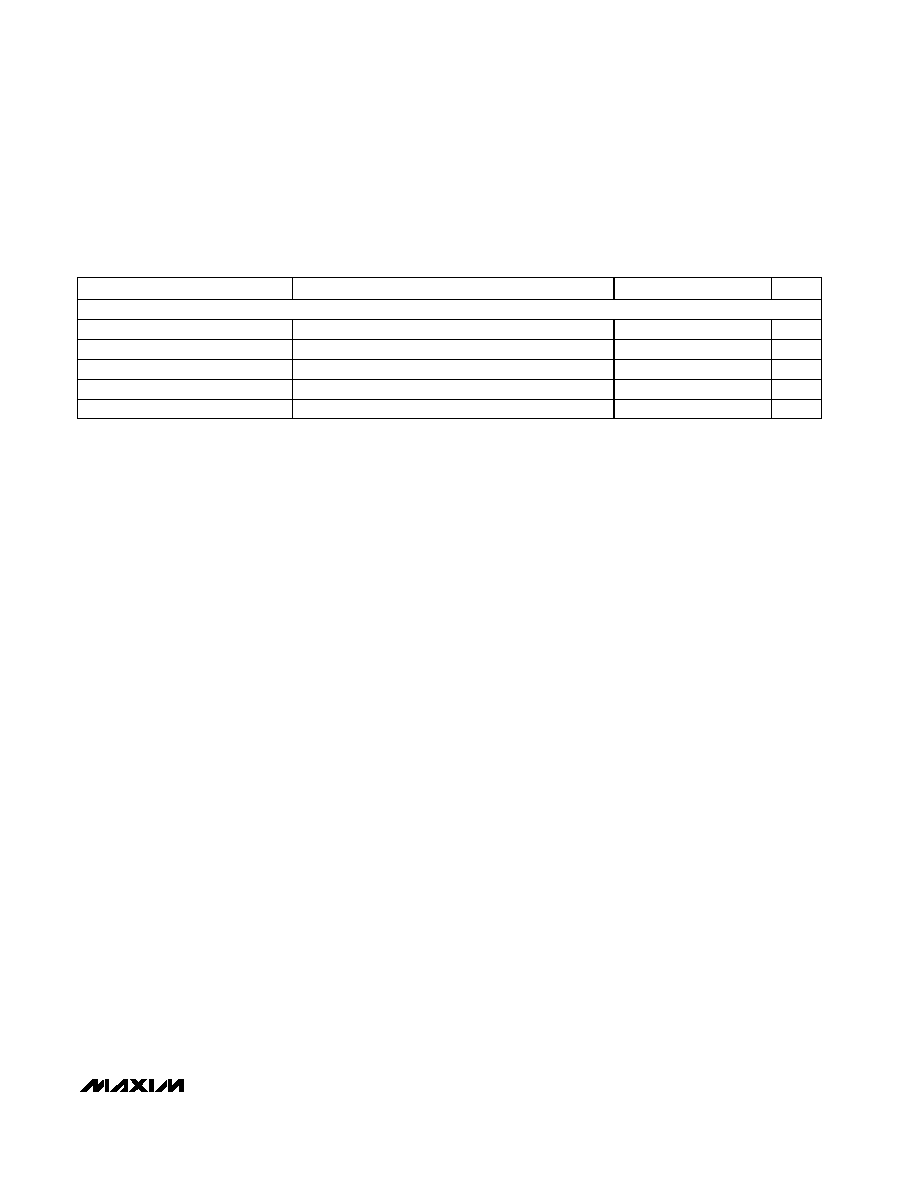
LO SECTION
LO Input Power
-12
-10
-5
dBm
LO Leakage at LNA Input
-40
dBm
LO Output Power
BUFFEN = high, 100
load
-10
-7
dBm
LO Output Noise Power
45MHz to 55MHz offset
-145
-143
dBc/Hz
LO Buffer Reverse Isolation
35
dB