 | ÐлекÑÑоннÑй компоненÑ: MAX2424 | СкаÑаÑÑ:  PDF PDF  ZIP ZIP |
Äîêóìåíòàöèÿ è îïèñàíèÿ www.docs.chipfind.ru
________________General Description
The MAX2424/MAX2426 highly integrated front-end ICs
provide the lowest cost solution for cordless and ISM-
band radios operating in the 900MHz band. Both devices
incorporate a receive image-reject mixer (to reduce filter
cost) as well as a versatile transmit mixer. The devices
operate from a +2.7V to +4.8V single power supply,
allowing direct connection to a 3-cell battery stack.
The receive path incorporates an adjustable-gain LNA
and an image-reject downconverter with 35dB image
suppression. These features yield excellent combined
downconverter noise figure (4dB) and high linearity with
an input third-order intercept point (IIP3) of up to +2dBm.
The transmitter consists of a double-balanced mixer and
a power amplifier (PA) predriver that produces up to
0dBm (in some applications serving as the final power
stage). It can be used in a variety of configurations,
including BPSK modulation, direct VCO modulation, and
transmitter upconversion. For devices featuring trans-
mit as well as receive image rejection, refer to the
MAX2420/MAX2421/MAX2422/MAX2460/MAX2463
data sheet.
The MAX2424/MAX2426 have an on-chip local oscillator
(LO), requiring only an external varactor-tuned LC tank
for operation. The integrated divide-by-64/65 dual-mod-
ulus prescaler can also be set to a direct mode, in which
it acts as an LO buffer amplifier. Four separate power-
down inputs can be used for system power manage-
ment, including a 0.5µA shutdown mode.
The MAX2424/MAX2426 come in a 28-pin SSOP pack-
age.
________________________Applications
Cordless Phones
Wireless Telemetry
Wireless Networks
Spread-Spectrum Communications
Two-Way Paging
____________________________Features
o
Receive Mixer with 35dB Image Rejection
o
Adjustable-Gain LNA
o
Up to +2dBm Combined Receiver Input IP3
o
4dB Combined Receiver Noise Figure
o
Optimized for Common Receiver IF Frequencies:
10.7MHz (MAX2424)
70MHz (MAX2426)
o
PA Predriver Provides up to 0dBm
o
Low Current Consumption: 23mA Receive
20mA Transmit
9.5mA Oscillator
o
0.5µA Shutdown Mode
o
Operates from Single +2.7V to +4.8V Supply
MAX2424/MAX2426
900MHz Image-Reject Receivers
with Transmit Mixer
________________________________________________________________
Maxim Integrated Products
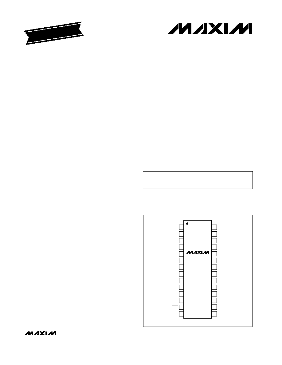
1
28
27
26
25
24
23
22
21
20
19
18
17
16
15
1
2
3
4
5
6
7
8
9
10
11
12
13
14
GND
GND
GND
TANK
TXON
PREOUT
PREGND
MOD
DIV1
VCOON
RXON
CAP2
TXIN
TXIN
LNAGAIN
TXOUT
GND
GND
RXIN
GND
RXOUT
CAP1
SSOP
TOP VIEW
MAX2424
MAX2426
TANK
V
CC
V
CC
V
CC
V
CC
V
CC
___________________Pin Configuration
19-1350 Rev 2; 2/99
PART
MAX2424
EAI
-40°C to +85°C
TEMP. RANGE
PIN-PACKAGE
28 SSOP
_______________Ordering Information
Functional Diagram appears at end of data sheet.
EVALUATION KIT MANUAL
FOLLOWS DATA SHEET
MAX2426
EAI
-40°C to +85°C
28 SSOP
For free samples & the latest literature: http://www.maxim-ic.com, or phone 1-800-998-8800.
For small orders, phone 1-800-835-8769.
MAX2424/MAX2426
900MHz Image-Reject Receiver
with Transmit Mixer
2
_______________________________________________________________________________________
ABSOLUTE MAXIMUM RATINGS
DC ELECTRICAL CHARACTERISTICS
(V
CC
= +2.7V to +4.8V, no RF signals applied, LNAGAIN = Unconnected, V
TXIN
= V
TXIN
= 2.3V, V
VCOON
= 2.4V, V
RXON
= V
TXON
=
V
MOD
= V
DIV1
= 0.45V, PREGND = GND, T
A
= -40°C to +85°C. Typicals are at T
A
= +25°C, V
CC
= 3.3V, unless otherwise noted.)
Stresses beyond those listed under "Absolute Maximum Ratings" may cause permanent damage to the device. These are stress ratings only, and functional
operation of the device at these or any other conditions beyond those indicated in the operational sections of the specifications is not implied. Exposure to
absolute maximum rating conditions for extended periods may affect device reliability.
Note 1:
Calculated by measuring the combined oscillator and prescaler supply current and subtracting the oscillator supply current.
Note 2:
Calculated by measuring the combined oscillator and LO buffer supply current and subtracting the oscillator supply current.
Note 3:
Calculated by measuring the combined receive and oscillator supply current and subtracting the oscillator supply current.
With LNAGAIN = GND, the supply current drops by 4.5mA.
Note 4:
Calculated by measuring the combined transmit and oscillator supply current and subtracting the oscillator supply current.
V
CC
to GND ...........................................................-0.3V to +5.5V
TXIN, TXIN Differential Voltage ..............................................+2V
Voltage on TXOUT......................................-0.3V to (V
CC
+ 1.0V)
Voltage on LNAGAIN, TXON, RXON, VCOON,
DIV1, MOD, TXIN, TXIN............................-0.3V to (V
CC
+ 0.3V)
RXIN Input Power..............................................................10dBm
TANK, TANK Input Power ...................................................2dBm
Continuous Power Dissipation (T
A
= +70°C)
SSOP (derate 9.50mW/°C above +70°C) ......................762mW
Operating Temperature Range ...........................-40°C to +85°C
Junction Temperature ......................................................+150°C
Storage Temperature Range .............................-65°C to +165°C
Lead Temperature (soldering, 10sec) .............................+300°C
PARAMETER
MIN
TYP
MAX
UNITS
Receive Supply Current (Note 3)
23
36
mA
Prescaler Supply Current
(buffer mode) (Note 2)
5.4
8.5
mA
Oscillator Supply Current
Supply-Voltage Range
2.7
4.8
V
9.5
14
mA
Prescaler Supply Current
(÷ 64/65 mode) (Note 1)
4.2
6
mA
CONDITIONS
V
RXON
= 2.4V, PREGND = unconnected
V
DIV1
= 2.4V
PREGND = unconnected
Digital Input Voltage Low
0.45
V
Shutdown Supply Current
0.5
RXON, TXON, DIV1, VCOON, MOD
VCOON = RXON = TXON
= MOD = DIV1 = GND
Digital Input Current
±1
±10
µA
Voltage on any one digital input = V
CC
or GND
Digital Input Voltage High
V
2.4
RXON, TXON, DIV1, VCOON, MOD
10
µA
T
A
= +25°C
T
A
= -40°C to +85°C
Transmitter Supply Current (Note 4)
20
32
mA
V
RXON
= 0.45V, V
TXON
= 2.4V,
PREGND = unconnected
AC ELECTRICAL CHARACTERISTICS
(MAX2424/MAX2426 EV kit, V
CC
= +3.3V, f
RXIN
= 915MHz, P
RXIN
= -35dBm, V
TXIN
= V
TXIN
= 2.3V (DC bias), V
TXIN
= 250mVp-p,
f
TXIN
= 1MHz, V
LNAGAIN
= 2V, V
VCOON
= 2.4V, RXON = TXON = MOD = DIV1 = PREGND = GND, T
A
= +25°C, unless otherwise noted.)
MAX2424/MAX2426
900MHz Image-Reject Receiver
with Transmit Mixer
_______________________________________________________________________________________
3
(Note 11)
MAX2424 (Notes 5, 6)
T
A
= T
MIN
to T
MAX
(Note 5)
T
A
= +25°C
(Notes 5, 6)
(Notes 5, 10)
(Note 9)
Receiver on or off
LNAGAIN = GND (Note 7)
V
LNAGAIN
= 1V (Note 7)
V
LNAGAIN
= 1V (Notes 5, 8)
LNAGAIN = V
CC
(Notes 5, 8)
V
LNAGAIN
= V
CC
,
T
A
= -40°C to +85°C (Notes 5, 7)
MAX2426 (Notes 5, 6)
V
LNAGAIN
= V
CC
,
T
A
= +25°C (Note 7)
V
LNAGAIN
= 1V (Notes 5, 7)
LNAGAIN = V
CC
(Notes 5, 7)
CONDITIONS
dBc
30
Carrier Suppression
dBm
3.5
Output Third-Order Intercept (OIP3)
dBm
-0.5
Output 1dB Compression
-10
-4.5
dBm
-9.5
-7
-5
Output Power
MHz
125
Baseband 3dB Bandwidth
MHz
800
1000
Output Frequency Range
ns
500
Receiver Turn-On Time
dBm
-60
LO to RXIN Leakage
-8
dB
-19
-17
Input Third-Order Intercept
(IIP3)
12
dB
4
5
Noise Figure
MHz
8.5
10.7
12.5
MHz
800
1000
Input Frequency Range
-16
12
18
24
19
25
55
70
85
IF Frequency Range
dB
26
35
Image Frequency Rejection
dB
20
22
24.5
Conversion Power Gain
19
21
23.5
UNITS
MIN
TYP
MAX
PARAMETER
MAX2424
MAX2426
MAX2424
MAX2426
V
LNAGAIN
= 1V
LNAGAIN = V
CC
-18
dBm
-26
Input 1dB Compression
(Note 12)
ns
220
Transmitter Turn-On Time
dBm/Hz
-140
Output Noise Density
RECEIVER
(V
RXON
= 2.4V, f
LO
= 925.7MHz (MAX2424), f
LO
= 985MHz (MAX2426))
TRANSMITTER
(V
TXON
= 2.4V, f
LO
= 915MHz)
V
DIV1
= 2.4V, Z
L
= 50
,
MAX2424/MAX2426
900MHz Image-Reject Receiver
with Transmit Mixer
4
_______________________________________________________________________________________
AC ELECTRICAL CHARACTERISTICS (continued)
(MAX2424/MAX2426 EV kit, V
CC
= +3.3V, f
RXIN
= 915MHz, P
RXIN
= -35dBm, V
TXIN
= V
TXIN
= 2.3V (DC bias), V
TXIN
= 250mVp-p,
f
TXIN
= 1MHz, V
LNAGAIN
= 2V, V
VCOON
= 2.4V, RXON = TXON = MOD = DIV1 = PREGND = GND, T
A
= +25°C, unless otherwise noted.)
PARAMETER
MIN
TYP
MAX
UNITS
Oscillator Phase Noise
Oscillator Frequency Range
800
1100
MHz
82
dBc/Hz
(Note 5)
CONDITIONS
Note 5:
Guaranteed by design and characterization.
Note 6:
Image rejection typically falls to 30dBc at the frequency extremes.
Note 7:
Refer to the
Typical Operating Characteristics for a plot showing Receiver Gain vs. LNAGAIN Voltage, Input IP3 vs.
LNAGAIN Voltage, and Noise Figure vs. LNAGAIN Voltage.
Note 8:
Two tones at P
RXIN
= -45dBm each, f1 = 915.0MHz and f2 = 915.2MHz.
Note 9:
Time delay from V
RXON
= 0.45V to V
RXON
= 2.4V transition to the time the output envelope reaches 90% of its final value.
Note 10:
Output power typically falls to -10dBm at the frequency extremes.
Note 11:
Two tones at V
TXIN
= 125mVp-p, f1 = 1.0MHz, and f2 = 1.2MHz.
Note 12:
Time delay from V
TXON
= 0.45V to V
TXON
= 2.4V transition to the time the output envelope reaches 90% of its final value.
Note 13:
Using tank components L3 = 5.0nH (Coilcraft A02T), C2 = C3 = C26 = 3.3pF, R6 = R7 = 10
.
Note 14:
This approximates a typical application in which TXOUT is followed by an external PA and a T/R switch with finite isolation.
Note 15:
Relative to the rising edge of PREOUT.
Prescaler Output Level
500
mVp-p
-11
-8
Required Modulus Setup Time
(Notes 5, 15)
10
ns
Z
L
= 100k
| |
10pF
÷
64/65 mode
Required Modulus Hold Time
(Notes 5, 15)
0
ns
÷
64/65 mode
Oscillator Buffer Output Level
(Notes 5, 13)
-12
dBm
V
DIV1
= 2.4V,
Z
L
= 50
10kHz offset (Note 13)
72
Standby to TX or Standby to RX
35
Oscillator Pulling
8
kHz
110
RX to TX with P
RXIN
=-45dBm (RX mode)
to P
RXIN
= 0dBm (TX mode) (Note 14)
MAX2424
MAX2426
MAX2424
MAX2426
MAX2424
MAX2426
70
T
A
= +25°C
T
A
= -40°C to +85°C
OSCILLATOR AND PRESCALER
MAX2424/MAX2426
900MHz Image-Reject Receiver
with Transmit Mixer
_______________________________________________________________________________________
5
28
32
30
38
36
34
42
40
24
26
-40
0
20
-20
40
60
80
RECEIVER SUPPLY CURRENT
vs. TEMPERATURE
MAX2424/6-01
TEMPERATURE (°C)
I
CC
(mA)
V
CC
= 2.7V
V
CC
= 3.3V
V
CC
= 4.8V
RXON = V
CC
PREGND = UNCONNECTED
INCLUDES OSCILLATOR
CURRENT
37
35
33
31
29
27
25
23
21
39
-40
0
20
-20
40
60
80
TRANSMITTER SUPPLY CURRENT
vs. TEMPERATURE
MAX2424/6-02
TEMPERATURE (°C)
I
CC
(mA)
V
CC
= 2.7V
V
CC
= 3.3V
V
CC
= 4.8V
TXON = V
CC
PREGND = UNCONNECTED
INCLUDES OSCILLATOR
CURRENT
0
1.0
0.5
2.5
2.0
1.5
4.0
3.5
3.0
4.5
-40
0
20
-20
40
60
80
SHUTDOWN SUPPLY CURRENT
vs. TEMPERATURE
MAX2424/6-03
TEMPERATURE (°C)
I
CC
(
µ
A)
V
CC
= 2.7V
V
CC
= 3.3V
V
CC
= 4.8V
VCOON = GND
25
20
15
10
5
0
-5
-10
-15
-20
0
0.5
1.0
1.5
2.0
RECEIVER GAIN vs. LNAGAIN
MAX2424/6-04
LNAGAIN VOLTAGE (V)
RECEIVER GAIN (dB)
ADJUSTABLE
GAIN
MAX
GAIN
LNA
PARTIALLY
BIASED
LNA
OFF
AVOID
THIS
REGION
RXON = V
CC
18
22
20
26
24
-40
0
20
-20
40
60
80
MAX2424
RECEIVER GAIN vs. TEMPERATURE
MAX2424/6-07
TEMPERATURE (°C)
RECEIVER GAIN (dB)
V
CC
= 2.7V
V
CC
= 3.3V
V
CC
= 4.8V
LNAGAIN = V
CC
RXON = V
CC
-20
-15
-10
-5
0
5
0
0.5
1.0
1.5
2.0
RECEIVER INPUT IP3 vs. LNAGAIN
MAX2424/6-05
LNAGAIN VOLTAGE (V)
IIP3 (dBm)
ADJUSTABLE
GAIN
AVOID
THIS
REGION
MAX
GAIN
LNA
PARTIALLY
BIASED
LNA
OFF
RXON = V
CC
0
5
15
10
25
20
30
40
35
0
0.5
1.0
1.5
2.0
RECEIVER NOISE FIGURE
vs. LNAGAIN
MAX2424/6-06
LNAGAIN VOLTAGE (V)
NOISE FIGURE (dB)
ADJUSTABLE
GAIN
AVOID
THIS
REGION
MAX
GAIN
LNA
PARTIALLY
BIASED
LNA
OFF
RXON = V
CC
DIV1 = V
CC
3.0
4.0
3.5
5.0
5.5
4.5
-40
0
20
-20
40
60
80
RECEIVER NOISE FIGURE vs.
TEMPERATURE AND SUPPLY VOLTAGE
MAX2424/6-08
TEMPERATURE (°C)
NOISE FIGURE (dB)
V
CC
= 3.3V
LNAGAIN = V
CC
RXON = V
CC
DIV1 = V
CC
V
CC
= 4.8V
V
CC
= 2.7V
-20
-16
-18
-8
-10
-6
-12
-14
-40
0
20
-20
40
60
80
RECEIVER INPUT IP3
vs. TEMPERATURE
MAX2424/6-09
TEMPERATURE (°C)
IIP3 (dBm)
V
LNAGAIN
= 1V
RXON = V
CC
V
LNAGAIN
= 2V
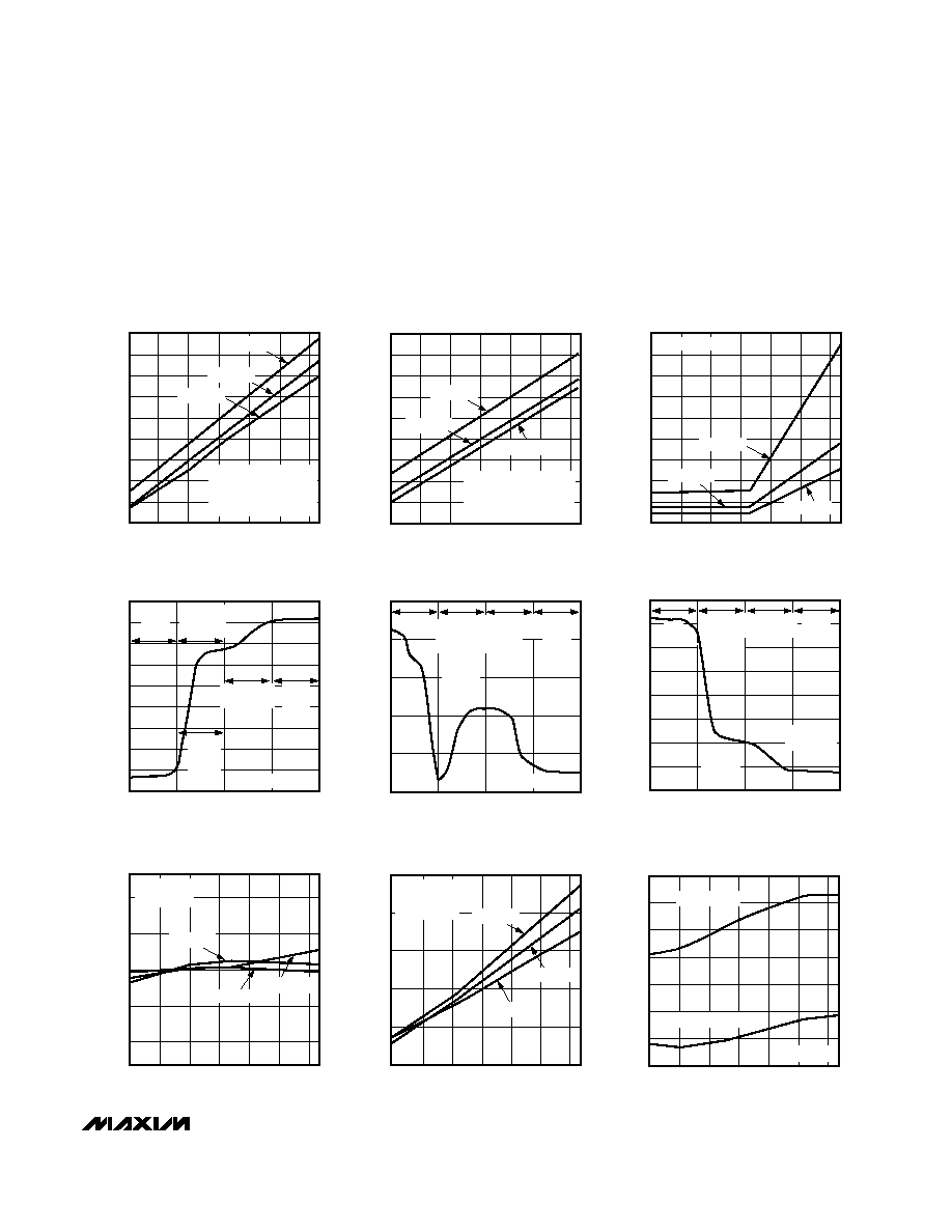
__________________________________________Typical Operating Characteristics
(MAX2424/MAX2426 EV kit, V
CC
= +3.3V; f
LO(RX)
= 925.7MHz (MAX2424), 985MHz (MAX2426); f
RXIN
= 915MHz, P
RXIN
=
-35dBm, f
LO(TX)
= 915MHz, V
TXIN
= V
TXIN
= 2.3V (DC bias), V
TXIN
= 250mVp-p, f
TXIN
= 1MHz, V
LNAGAIN
= 2V, V
VCOON
= 2.4V,
RXON = TXON = MOD = DIV1 = PREGND = GND, T
A
= +25°C, unless otherwise noted.)