 | –≠–ª–µ–∫—Ç—Ä–æ–Ω–Ω—ã–π –∫–æ–º–ø–æ–Ω–µ–Ω—Ç: MAX2473 | –°–∫–∞—á–∞—Ç—å:  PDF PDF  ZIP ZIP |

For free samples & the latest literature: http://www.maxim-ic.com, or phone 1-800-998-8800.
For small orders, phone 1-800-835-8769.
General Description
The MAX2472/MAX2473 are flexible, wideband, high-
reverse-isolation buffer amplifiers. The MAX2472 has dual
open-collector outputs capable of delivering -5dBm into
50
while maintaining harmonic suppression below
-25dBc. The MAX2473 has a single open-collector output
with a bias control pin to vary output power from -10dBm
to -2dBm while maintaining harmonic suppression below
-25dBc. The MAX2472/MAX2473's combination of high
reverse isolation and low supply current makes them ideal
for applications requiring high performance with low
power. They feature high input impedance and open-col-
lector outputs for maximum flexibility, enabling them to be
used with a variety of oscillator topologies.
Both the MAX2472 and MAX2473 operate from a single
+2.7V to +5.5V supply. With V
CC
= +3.0V and -25dBm
input power, the MAX2472 consumes 5.2mA, while the
MAX2473 consumes only 2.7mA. Both devices are avail-
able in a tiny 6-pin SOT23 package requiring minimal
board space.
Applications
Cellular and PCS Mobile Phones
Private Mobile Radios
ISM-Band Applications
IF/RF Oscillators
General-Purpose Buffers/Amplifiers
Typical Operating Circuits appear at end of data sheet.
Features
o
+2.7V to +5.5V Supply Range
o
500MHz to 2500MHz Input Frequency Range
o
High Reverse Isolation: 49dB at 900MHz
o
Dual Open-Collector Outputs (MAX2472)
o
Adjustable -10dBm to -2dBm Output Power
Control (MAX2473)
o
High Input Impedance: >250
at 900MHz
o
Ultra-Small SOT23-6 Package
MAX2472/MAX2473
500MHz to 2500MHz
VCO Buffer Amplifiers
________________________________________________________________
Maxim Integrated Products
1
Functional Diagrams
19-1466; Rev 0; 6/99
PART
MAX2472
EUT-T
MAX2473
EUT-T -40∞C to +85∞C
-40∞C to +85∞C
TEMP.
RANGE
PIN-
PACKAGE
6 SOT23-6
6 SOT23-6
EVALUATION KIT MANUAL
FOLLOWS DATA SHEET
Ordering Information
SOT
TOP MARK
AAAZ
AABA
GND
GND
OUT2
OUT1
IN
V
CC
MAX2472
BIAS
GND
GND
BIAS
OUT
IN
V
CC
MAX2473
BIAS
GND
IN
OUT2 (BIAS)
1
6
V
CC
5
GND
OUT1 (OUT)
MAX2472
MAX2473
SOT23-6
TOP VIEW
( ) ARE FOR MAX2473.
2
3
4
Pin Configuration

MAX2472/MAX2473
500MHz to 2500MHz
VCO Buffer Amplifiers
2
_______________________________________________________________________________________
ABSOLUTE MAXIMUM RATINGS
DC ELECTRICAL CHARACTERISTICS
(V
CC
= +2.7V to +5.5V, P
IN
= -25dBm, IN driven from a 50
source, OUT_ LC-matched to 50
, T
A
= T
MIN
to T
MAX
, unless otherwise
noted. Typical values are at V
CC
= +3V, T
A
= +25∞C.) (Note 1)
AC ELECTRICAL CHARACTERISTICS--MAX2472
(
Typical Operating Circuits, V
CC
= +3V, P
IN
= -25dBm, IN driven from a 50
source, OUT1 and OUT2 LC matched to 50
, T
A
=
+25∞C, unless otherwise noted.)
Stresses beyond those listed under "Absolute Maximum Ratings" may cause permanent damage to the device. These are stress ratings only, and functional
operation of the device at these or any other conditions beyond those indicated in the operational sections of the specifications is not implied. Exposure to
absolute maximum rating conditions for extended periods may affect device reliability.
V
CC
to GND ..............................................................-0.3V to +7V
OUT1, OUT2, BIAS to GND........................-0.3V to (V
CC
+ 0.3V)
Maximum BIAS Pin Current................................................150µA
Maximum Input Power....................................................+10dBm
Continuous Power Dissipation
SOT23-6 (derate 8.7mW/∞C above +70∞C)...................696mW
Operating Temperature Range ...........................-40∞C to +85∞C
Junction Temperature ......................................................+150∞C
Storage Temperature Range .............................-65∞C to +150∞C
Lead Temperature (soldering, 10sec) .............................+300∞C
CONDITIONS
2.7
mA
5.2
8.0
I
CC
V
2.7
5.5
V
CC
Input Voltage Range
Supply Current
4.8
5.1
2.5
4.3
UNITS
MIN
TYP
MAX
SYMBOL
PARAMETER
MAX2473, R
BIAS
= 23k
MAX2473, R
BIAS
= 11k
MAX2472
No drive
MAX2472
MAX2473, R
BIAS
= 23k
MAX2473, R
BIAS
= 11k
dBm
S
12
2
S
21
2
f
IN
= 900MHz, T
A
= +25∞C
Transducer Gain
(IN to OUT2)
f
IN
= 600MHz
f
IN
= 900MHz
dB
9.2
f
IN
= 900MHz
f
IN
= 2400MHz
f
IN
= 1900MHz
f
IN
= 600MHz
40
f
IN
= 1900MHz
f
IN
= 2400MHz
f
IN
= 900MHz
f
IN
= 900MHz, T
A
= T
MIN
to T
MAX
(Note 3)
CONDITIONS
dB
6.6
14.6
f
IN
= 600MHz
13.0
S
21
2
f
IN
= 2400MHz
5.3
f
IN
= 1900MHz
6.8
Transducer Gain
(IN to OUT1)
dB
7.8
10.2
12.2
14.0
MHz
500
2500
f
IN
Input Frequency Range (Note 2)
26
30
43
Reverse Isolation
(IN to OUT2)
7.5
6.0
-3.2
P
OUT1dB
Output 1dB Compression Point
UNITS
MIN
TYP
MAX
SYMBOL
PARAMETER
MAX2472/MAX2473
500MHz to 2500MHz
VCO Buffer Amplifiers
_______________________________________________________________________________________
3
Note 1:
Limits are 100% production tested at T
A
= +25∞C. Limits over the entire operating temperature range are guaranteed by
design and characterization but are not production tested.
Note 2:
This is the recommended operating frequency range. The parts have been characterized over the specified frequency
range and production tested at 900MHz. Operation outside of this range is possible but not guaranteed.
Note 3:
Guaranteed by design and characterization.
P
OUT
= -5dBm, f
IN
= 900MHz
f
IN
= 900MHz
f
IN
= 1900MHz
f
IN
= 900MHz
CONDITIONS
dBc
-25
dB
24
Isolation (OUT1 to OUT2)
10.2
9.5
NF
Noise Figure
UNITS
MIN
TYP
MAX
SYMBOL
PARAMETER
Harmonic Suppression
dB
f
IN
= 900MHz, T
A
= +25∞C
f
IN
= 600MHz
f
IN
= 1900MHz
f
IN
= 900MHz
P
OUT
= -5dBm, f
IN
= 900MHz
f
IN
= 600MHz
f
IN
= 1900MHz
f
IN
= 2400MHz
f
IN
= 900MHz
f
IN
= 900MHz
f
IN
= 2400MHz
CONDITIONS
Harmonic Suppression
dB
dBc
-25
9.2
dB
29
NF
Noise Figure
6.8
11.8
16.8
14.8
S
21
2
MHz
500
2500
f
IN
Input Frequency Range (Note 2)
35
S
12
2
48
50
Reverse Isolation
7.6
7.2
-6.0
P
OUT1dB
Output 1dB Compression Point
UNITS
MIN
TYP
MAX
SYMBOL
PARAMETER
AC ELECTRICAL CHARACTERISTICS--MAX2473
(
Typical Operating Circuits, V
CC
= +3V, P
IN
= -25dBm, R
BIAS
= 15k
, IN driven from a 50
source, OUT LC matched to 50
, T
A
=
+25∞C, unless otherwise noted.)
dBm
-0.9
R
BIAS
= 23k
R
BIAS
= 11k
f
IN
= 1900MHz
9.9
Transducer Gain
dB
f
IN
= 900MHz, T
A
= T
MIN
to T
MAX
(Note 3)
6.4
19.0
S
12
2
f
IN
= 900MHz
f
IN
= 2400MHz
f
IN
= 1900MHz
f
IN
= 600MHz
49
dB
30
34
54
Reverse Isolation
(IN to OUT1)
AC ELECTRICAL CHARACTERISTICS--MAX2472 (continued)
(
Typical Operating Circuits, V
CC
= +3V, P
IN
= -25dBm, IN driven from a 50
source, OUT1 and OUT2 LC matched to 50
, T
A
=
+25∞C, unless otherwise noted.)
MAX2472/MAX2473
500MHz to 2500MHz
VCO Buffer Amplifiers
4
_______________________________________________________________________________________
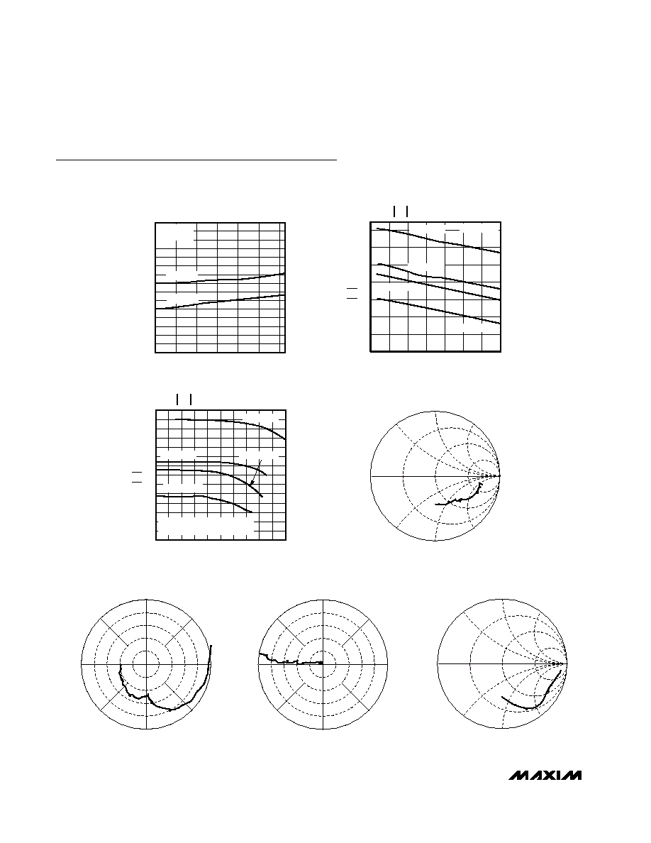
Typical Operating Characteristics
(MAX2472/MAX2473 EV kit, V
CC
= +3V, T
A
= +25∞C, unless otherwise noted.)
5.0
4.0
6.0
7.0
-40
-20
0
20
40
60
80
SUPPLY CURRENT vs. TEMPERATURE
MAX2472 toc01
TEMPERATURE (∞C)
I
CC
(mA)
P
IN
= -20dBm
f
IN
= 900MHz
V
CC
= 3V
V
CC
= 5V
0
4
2
10
8
6
14
12
-50
10
30
-30
-10
50
70
90
S
21
2
vs. TEMPERATURE
MAX2472 toc02
TEMPERATURE (∞C)
f
IN
= 600MHz
f
IN
= 900MHz
f
IN
= 1900MHz
f
IN
= 2400MHz
P
IN
= -20dBm
S
21
2
(dB)
0
2
4
6
10
8
12
14
-20
-16 -14
-18
-12 -10 -8
-6
-4
-2
0
S
21
2
vs. OUTPUT POWER
MAX2472 toc03
P
OUT
(dBm)
FOR OUT1 WITH OUT2 REACTIVELY
MATCHED AND TERMINATED
f
IN
= 600MHz
f
IN
= 900MHz
f
IN
= 2400MHz
S
21
2
(dB)
f
IN
= 1900MHz
S
21
MAX2472 toc07
A
C
B
D
(3 UNITS FULL SCALE)
FOR OUT2 WITH OUT1 BIASED
AND TERMINATED
A: f
IN
= 600MHz
B: f
IN
= 900MHz
C: f
IN
= 1900MHz
D: f
IN
= 2400MHz
S
11
MAX2472 toc06
A
C
B
D
FOR OUT2 WITH OUT1 BIASED
AND TERMINATED
A: f
IN
= 600MHz
B: f
IN
= 900MHz
C: f
IN
= 1900MHz
D: f
IN
= 2400MHz
S
12
MAX2472 toc08
A
C
B
D
(0.1 UNITS FULL SCALE)
FOR OUT2 WITH OUT1 BIASED
AND TERMINATED
A: f
IN
= 600MHz
B: f
IN
= 900MHz
C: f
IN
= 1900MHz
D: f
IN
= 2400MHz
S
22
MAX2472 toc09
A
C
B
D
FOR OUT2 WITH OUT1 BIASED
AND TERMINATED
A: f
IN
= 600MHz
B: f
IN
= 900MHz
C: f
IN
= 1900MHz
D: f
IN
= 2400MHz
MAX2472
MAX2472/MAX2473
500MHz to 2500MHz
VCO Buffer Amplifiers
_______________________________________________________________________________________
5
Typical Operating Characteristics (continued)
(MAX2472/MAX2473 EV kit, V
CC
= +3V, T
A
= +25∞C, unless otherwise noted.)
MAX2472
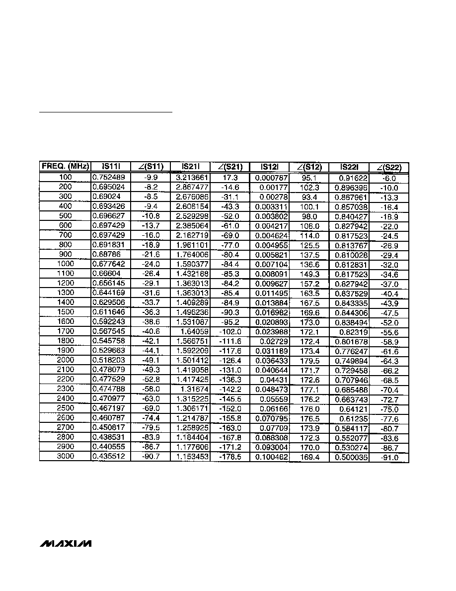
SCATTERING PARAMETERS
(IN to OUT 2)