MAX2510 EV DS
General Description
The MAX2510 evaluation kit (EV kit) simplifies testing of
the MAX2510 low-power IF transceiver with limiter/
received-signal-strength indicator (RSSI) and quadra-
ture modulator. This EV kit allows simple evaluation of
all chip functions in a 50
test environment.
Features
o +2.7V to +5.5V Single-Supply Operation
o Allows Testing of Advanced Power Management
(four modes):
< 1nA Shutdown
Receive
Transport
Standby
o 50 SMA Connector Interface
o Fully Assembled and Tested
Evaluates: MAX2510
MAX2510 Evaluation Kit
________________________________________________________________ Maxim Integrated Products
1
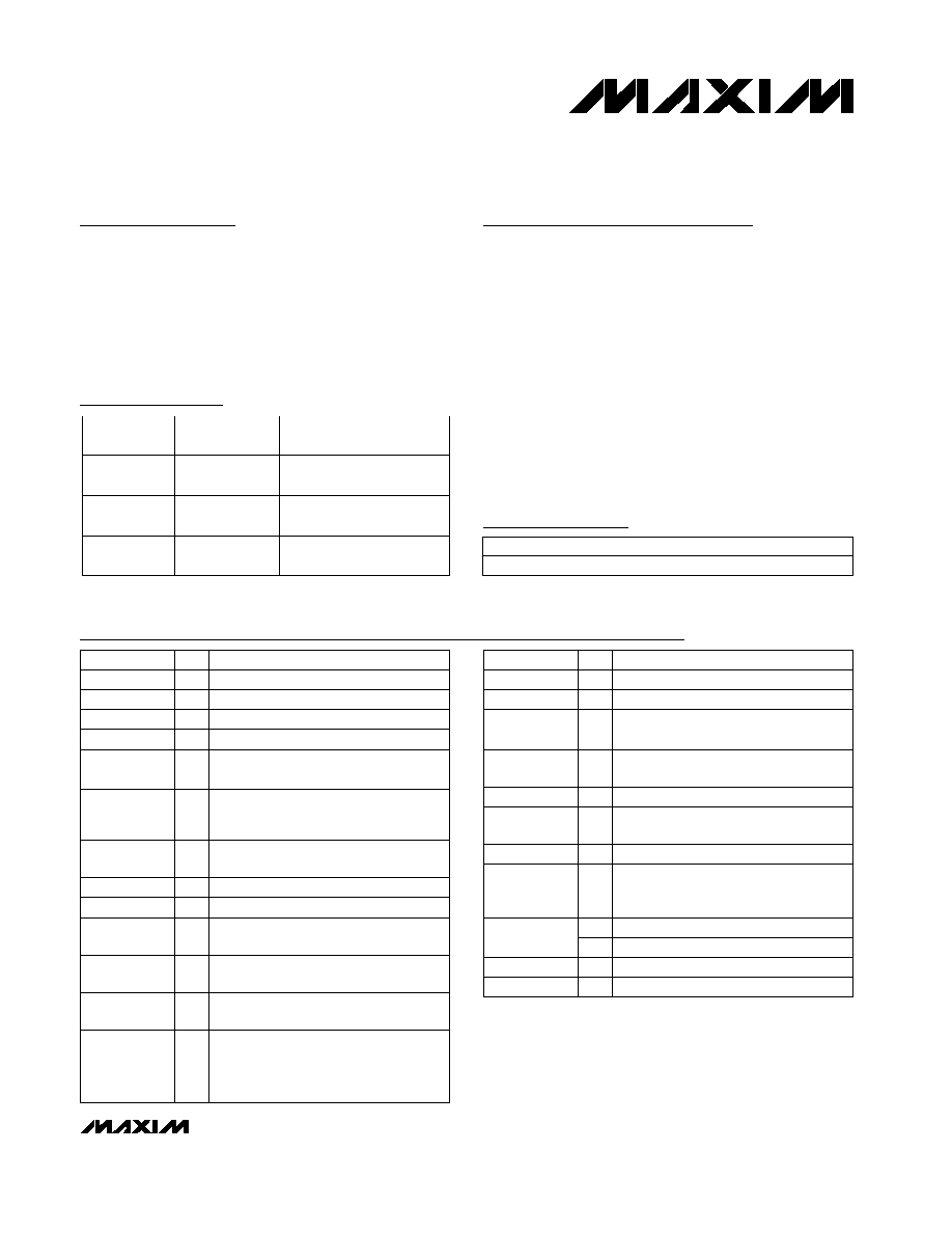
PART
TEMP. RANGE
IC PACKAGE
MAX2510EVKIT-SO
-40°C to +85°C
28 QSOP
SUPPLIER
PHONE/
FAX
INTERNET
Coilcraft
(847) 639-6400/
(847) 639-1469
http://www.coilcraft.com
Component Suppliers
Component List
Ordering Information
Murata-Erie
(814) 237-1431/
(814) 238-0490
http://www.murata.com
Sprague
(603) 224-1961/
(603) 224-1430
--
DESIGNATION QTY
DESCRIPTION
C1, C3
2
0.01µF capacitors
C2
1
330pF ceramic capacitor
C4
1
0.047µF capacitor
C6, C8
2
47pF capacitors (0603)
C7, C9, C12,
C13, C21, C22,
C23, C27
8
0.1µF capacitors
C18, C25
2
10pF capacitors (0603)
C20, C29
2
0.022µF capacitors
C24
1
10µF tantalum capacitor
Sprague 293D106X0010C2
L2
1
82nH inductor
Coilcraft 0805HS-820TKBC
L3, L4
2
47nH inductors
Coilcraft 0805HS-470TKBC
LO IN, I, Q,
RXIN, RXIN,
TXOUT, TXOUT,
MIXOUT, LIMIN
9
50
edge-mount SMA connectors
E.F. Johnson 142-0701-801
DESIGNATION QTY
DESCRIPTION
R3, R11, R17
3
50
resistors
R4, R7, R8, R14
4
5k
resistors
R1, R5
2
0
shorts (0603) (can be changed to
allow for other matching networks)
R9
1
Resistor--not installed (for back-
terminating an interstage filter)
R10, R15
2
280
1% resistors
R16
1
Resistor--not installed (for adjusting
the RSSI output voltage range)
U1
1
MAX2510EEI (28 QSOP)
U2
1
10.7MHz ceramic bandpass filter
(Z
O
= 330
), 3-pin through-hole footprint
Murata SFE10.7MA5-A
RXEN, TXEN
2
3-pin headers (0.1" center)
None
1
MAX2510EEI data sheet
Note: All resistors, capacitors, and inductors are surface-
mount components with an 0805 footprint, unless otherwise
specified. Filter U2 and the various jumpers are through-hole
mounted.
C14, C15,
C17, C19
4
0.001µF capacitors
2
Shunts
None
1
MAX2510EV-SO circuit board
C5, C10,
C30, C31
0
Not installed
19-1296; Rev 2; 1/01
For price, delivery, and to place orders, please contact Maxim Distribution at 1-888-629-4642,
or visit Maxim's website at www.maxim-ic.com.

Evaluates: MAX2510
MAX2510 Evaluation Kit
2
_______________________________________________________________________________________
_________________________Quick Start
The following section provides instructions for operating
the EV kit as an IF transceiver. The RF ports (RXIN,
RXIN, TXOUT, and TXOUT) are matched to 50
at
240MHz, and the second IF is configured for 10.7MHz
operation. The EV kit and the MAX2510 can be config-
ured for operation at other frequencies (see the
Detailed Description section and the MAX2510 data
sheet).
Test Equipment Required
This section lists the test equipment recommended for
verifying operation of the MAX2510. It is intended only
as a guide; some substitutions may be possible.
· Two RF-signal generators capable of delivering at
least 0dBm of output power up to 500MHz
(HP8656B, HP8648A, or equivalent). One generator
is required for the local oscillator (LO) source in
both transmit (Tx) and receive (Rx) modes. The
other is required for the Rx input signal in Rx mode.
· An RF spectrum analyzer that can cover the trans-
mitter's output frequency range, as well as a few
harmonics (HP8560E, for example).
· A baseband-signal generator that can produce two
outputs in quadrature (sine and cosine waves) at
levels of approximately 500mVp-p. This is neces-
sary to evaluate the transmitter's sideband suppres-
sion. The HP8904A/Opt. 002 generator provides
sine and cosine outputs at frequencies up to
600kHz.
· Optional: An RF 180° hybrid combiner or balun
(Anzac H-9 or equivalent). This is used for differen-
tial coupling into the RXIN, RXIN connections on the
receiver or the TXOUT, TXOUT connections on the
transmitter. If a balun is not available, these inputs
and outputs can be evaluated in a single-ended
configuration, at a slight performance cost.
· A voltmeter for measuring the RSSI output voltage.
· An oscilloscope for observing the limiter output
signals.
· A power supply that can provide up to 50mA at
+2.7V to +5.5V.
· Two 0V to 5V adjustable voltage sources for provid-
ing gain-control (GC) pin voltage and the VBIAS
voltage for the I and Q inputs.
· Two 50
SMA terminators
· Several 50
SMA cables
Connections and Setup
This section provides step-by-step instructions for get-
ting the EV kit up and running in both Tx and Rx modes.
Tx Mode
Perform the following steps to set up the EV kit in Tx
mode:
1) Make the DC connections: set the power supply to
3V, and connect it to the VCC and GND terminals
on the EV kit. Set one of the voltage sources to
1.4V, and connect it to VBIAS. Set the other voltage
source to 2V, and connect it to the gain-control ter-
minal (marked GC).
2) Set the part in Tx mode by putting 3-pin jumper
TXEN in the "high" position, and jumper RXEN in the
"low" position.
3) The supply current should be near 30mA. If this is
not the case, check the voltage on the TXEN and
RXEN test points. The TXEN voltage should be at
V
CC
, and the RXEN voltage should be at ground.
4) Connect TXOUT to the spectrum analyzer using an
SMA cable. Terminate TXOUT with a 50
SMA ter-
minator.
For differential operation, TXOUT and TXOUT can
be combined using a balun. Connect the balun's
output to the spectrum analyzer. Set the spectrum
analyzer to 240MHz center frequency with a 1MHz
total span.
5) Connect the local oscillator (LO) signal source to
the LO SMA connector. Set the frequency to
240MHz and the amplitude to -13dBm. You will see
a small amount of LO signal present at the center of
the spectrum-analyzer display.
6) Set both channels of the baseband-signal genera-
tor to deliver sine waves at 500mVp-p at a fre-
quency of 100kHz. To achieve maximum sideband
suppression, be sure that there is a precise 90°
phase difference between these two sinusoidal
signals. Connect the first signal to the I input. You
will see a double sideband signal (DSB) on the
spectrum analyzer at 240MHz, with the lower side-
band at (240MHz - 100kHz) and the upper side-
band at (240MHz + 100kHz). Connect the other
signal to the Q input. If the phase difference is set
correctly, you will see a cancellation of the side-
bands. Which sideband is canceled depends on
which input leads the other in phase. Swapping
the I and Q connections at the board's input sup-
presses one or the other sideband. Leave the part
set to transmit the upper sideband (USB) when fin-
ished. The rest of these instructions assume the

Evaluates: MAX2510
MAX2510 Evaluation Kit
_______________________________________________________________________________________
3
transmitter is set in USB mode and the lower side-
band (LSB) is the suppressed sideband. If the
application requires LSB, reverse the relevant
instructions. The EV kit also accommodates differ-
ential I and Q inputs. (Refer to the Detailed
Description section.)
7) The USB output power should be approximately
0dBm with GC = 2V. Test the GC function by slowly
lowering the voltage on the GC pin from 2V to 0V.
You will see at least a 40dB change in USB power
over this voltage range.
8) When the transmitter is working properly, you may
wish to test other features, such as shutdown mode
(both TXEN and RXEN jumpers set to "low". The I
and Q inputs can be adjusted to check transmitter
gain over frequency, VBIAS voltage, etc.
Rx Mode
This section describes how to connect and use the
MAX2510's receiver section.
1) Remove the I and Q input signal sources to prevent
crosstalk into the receiver during Rx-mode mea-
surements. The GC and VBIAS voltage supplies
have no function in Rx mode.
2) Switch the part into Rx mode by moving the RXEN
jumper to the "high" position and the TXEN jumper
to the "low" position.
3) Change the LO frequency to equal the desired Rx
frequency minus 10.7MHz. This provides a
10.7MHz downconverted signal into the off-chip fil-
ter (a 10.7MHz bandpass type). For a 240MHz Rx
frequency, the LO frequency should be (240 - 10.7
= 229.3 MHz). Leave the LO power level at -13dBm.
4) Connect RXIN to a second RF-signal generator
using an SMA cable. Terminate RXIN with 50
.
For differential operation, connect the signal gener-
ator to RXIN and RXIN through a balun. Set this
generator's frequency to 240MHz at -30dBm of out-
put power.
5) Connect an oscilloscope to the limiter outputs
LIMOUT and LIMOUT. A 2-channel oscilloscope
with low-capacitance probes is ideal. The signals
from LIMOUT and LIMOUT should be approximate-
ly 600mVp-p and out-of-phase with each other.
6) Connect a voltmeter to the RSSI test pad in the
upper-left corner of the EV kit to monitor the RSSI
output voltage. For -30dBm of RXIN power, the
RSSI voltage should be 1.8V. Lower the input power
in 10dBm steps, observing the decrease in RSSI
output voltage of about 20mV per 1dB change in
input power. Return the power level to -30dBm.
7) Observe that the signals at LIMOUT and LIMOUT
remain at constant level over the RXIN power range.
Advanced System
Power-Management Features
Besides the Tx and Rx modes previously mentioned, the
MAX2510 supports two other operating modes: shutdown
and standby. Bring both TXEN and RXEN jumpers to the
"low" position, putting the part in shutdown mode and
reducing the supply current to 2.0µA (typical).
To enter standby mode, bring both TXEN and RXEN
jumpers to the "high" position. This reduces the supply
current to about 0.5µA while leaving the VREF generator
active (for fast switching into receive mode).
_______________Detailed Description
The following section covers the EV kit's circuit design
in detail. (See the MAX2510 data sheet for additional
information.)
Baseband Inputs
The I, I, Q, and Q pins comprise the quadrature modu-
lator's baseband inputs. They require external DC bias-
ing to set a common-mode level of approximately 1.4V.
On the EV kit, this voltage is provided by external resis-
tors and a voltage supply (VBIAS). The I and Q pins are
AC coupled to SMA connectors, which induces a high-
pass cutoff of approximately 300Hz. The I and Q pins
are biased to the common-mode voltage and AC
grounded. Test points on the EV kit allow flexible
access to these pins if the application requires differen-
tial drive.
Transmitter Output
The MAX2510's Tx outputs (TXOUT and TXOUT) are
high-impedance open collectors; therefore, external
inductors are used for proper biasing. DC-blocking
capacitors are used to connect to these outputs. The
inductors and capacitors act only to provide biasing;
they do not set the output impedance. For single-ended
applications, terminate TXOUT with a 50
terminator.
Alternatively, replace L4 with a 0
short. Refer to the
MAX2510 data sheet for more information on matching
this port.
Receiver Input
The Rx inputs (RXIN and RXIN) require an impedance-
matching network for optimum performance. The Rx
inputs are matched to 240MHz on the EV kit as
shipped. The input matching network comprises a
series capacitor from each Rx input SMA connector to
the part, as well as a shunt inductor across RXIN and
RXIN. The EV kit layout provides space for additional
components: one series element on each side and a

Evaluates: MAX2510
MAX2510 Evaluation Kit
4
_______________________________________________________________________________________
shunt element across the inputs. The additional series
elements have been replaced by 0
shorts, and the
additional shunt element is not installed. Refer to the
MAX2510 data sheet for more information on designing
a matching network for this port.
Receiver Output
The receive downconverter mixer's output appears at
the MIXOUT pin (a current source that can drive a
165
load to 2Vp-p). The MIXOUT pin is terminated
with a net 330
(R10 + R11) for proper match to the
bandpass filter (Z
O
= 330
). Therefore, the net load at
MIXOUT is 330
330 = 165.
The EV kit design allows separate testing of the
MAX2510's Rx mixer and limiter sections for testing the
Rx mixer only. Coupling capacitor C20 is used to con-
nect the node between R10 and R11 to an external
SMA connector (MIXOUT). For these tests, the filter
(U2) must be removed, and R10 replaced with a 140
resistor. This network has some attenuation, but pre-
sents the correct impedance to the MIXOUT pin and
provides a nearly 50
output impedance for measure-
ment. The attenuation is 11.2dB.
Limiter Input
The MAX2510 EV kit can be modified to allow separate
testing of the limiter only, similar to the receive mixer in
the previous section. The filter (U2) must be removed.
This allows the limiter SMA connector to be used as a
direct input to the limiter.
Limiter Output
The downconverted, limited signal appears at the
LIMOUT and LIMOUT pins as a 1.2Vp-p differential
voltage (600mVp-p per side). For single-ended use, the
unused side can be left open. The limiter outputs can
deliver this voltage across a load as low as 250
.
______________________Layout Issues
A good PC board is an essential part of an RF circuit
design. The EV kit PC board can serve as a guide for
laying out a board using the MAX2510.
Rx Inputs and Tx Outputs
The layout of the RXIN and RXIN input matching net-
work should be layed out symmetrically to provide the
best input balance if used as a differential input. The
TXOUT and TXOUT biasing networks should also be
layed out symmetrically to present an equal load
impedance on each pin.
Baseband Inputs
The MAX2510's I, I, Q, and Q inputs are high imped-
ance; take care to minimize potential unwanted cou-
pling into these pins. The easiest way to accomplish
this is to keep the trace length to a minimum.
Power-Supply Decoupling
Each V
CC
node on a PC board should have its own
0.047µF decoupling capacitor. This minimizes supply
coupling from one section of the MAX2510 to another.
A star topology for the supply layout, in which each
V
CC
node on the MAX2510 circuit has a separate con-
nection to a central V
CC
node, can further minimize
coupling between sections of the MAX2510.
Evaluates: MAX2510
MAX2510 Evaluation Kit
_______________________________________________________________________________________
5
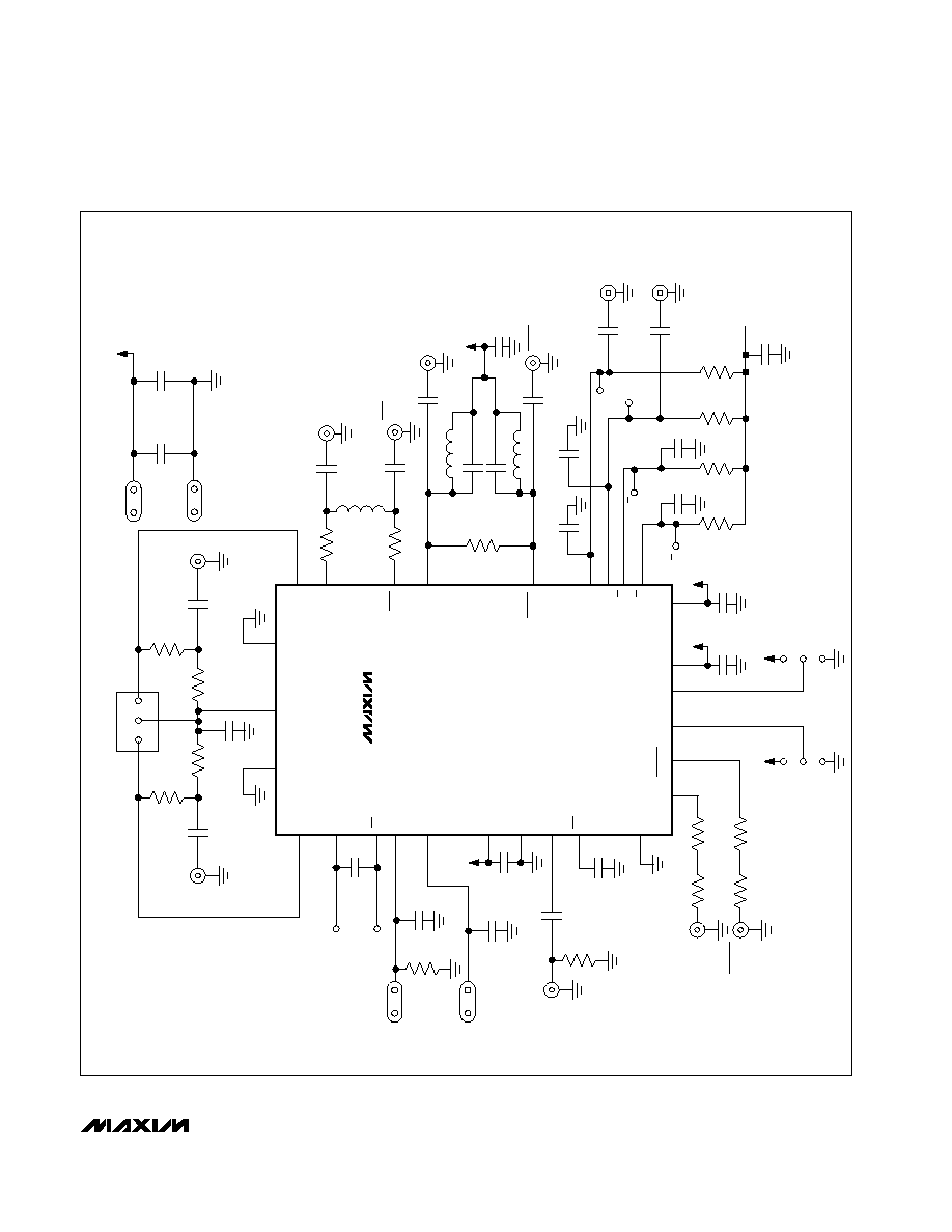
U1
MAX2510
C7
0.1
µ
F
C27
0.1
µ
F
R4
5k
R8
5k
R14
5k
R7
5k
I
I
Q
C12
0.1
µ
F
CZ
C1
0.01
µ
F
LIMIN
LIMIN
SMA
3
2
1
MURATA FILTER
SFE10.7MA5-A
V
CC
GND
V
CC
MIXOUT
SMA
C2
10
µ
F
C23
0.1
µ
F
R15
280
R10
280
C21
0.1
µ
F
GND
VREF
GND
MIXOUT
RXIN
RXIN
TXOUT
TXOUT
Q
I
I
Q
18
16
17
15
13
14
11
12
19
21
1
2
HIGH
HIGH
LOW
LOW
JU9
RXEN
R2
0
R6
0
R13
0
C6
47pF
C29
0.022
µ
F
C20
0.022
µ
F
C17
50
R11
50
R12
0
JU8
TXEN
3
1
2
3
24
22
25
RXIN
SMA
V
CC
TXOUT
SMA
TXOUT
SMA
L3, 47nH
L4, 47nH
L2
82nH
C25
10pF
C18
10pF
R1, 0
R5, 0
27
23
VIL
VA
RXEN
TXEN
LIMOUT
LIMOUT
GND
LO
LO
GND
V
CC
V
CC
GC
RSSI
CZ
2
26
28
20
1
TP1
TP2
RSSI
GC
LO
SMA
LIMOUT
SMA
LIMOUT
SMA
47pF
C8
R3
50
C3
0.01
µ
F
C2
300pF
R16
OPEN
C4
0.047
µ
F
10
9
6
7
8
5
4
3
C5
OPEN
R9
OPEN
C10
OPEN
C19
0.001
µ
F
C14
0.001
µ
F
C15
0.001
µ
F
C9
0.1
µ
F
C13
0.1
µ
F
C30, 20pF
C31, 20pF
C22
0.1
µ
F
RXIN
SMA
I
SMA
Q
SMA
V
CC
V
CC
VBIAS
V
CC
V
CC
Q
U2
Figure 1. MAX2510 EV Kit Schematic