General Description
The MAX2530/MAX2531/MAX2538 evaluation kits (EV
kits) simplify evaluation of the MAX2351/MAX2354/
MAX2358/MAX2359/MAX2530/MAX2531/MAX2537/
MAX2538 high-performance, silicon germanium (SiGe)
BiCMOS, quad-mode LNA/mixer ICs. They enable test-
ing of the devices' RF performance and require no
additional support circuitry. The signal inputs and out-
puts use SMA connectors to simplify the connection of
RF test equipment.
The MAX2530/MAX2531/MAX2538 EV kits are assem-
bled with an associated IC and incorporate input- and
output-matching components optimized for the 869MHz
to 894MHz cellular frequency band, 1930MHz to
1990MHz PCS frequency band, 1575.42MHz GPS fre-
quency band, and 183.6MHz IF output frequency. All
matching components can be changed to work at other
frequencies.
Use the Evaluation Kit Selector Guide to determine which
EV kit to order based on the application. For example,
to evaluate the MAX2354, use the MAX2530EVKIT.
Features
o 50 SMA Ports for Easy Testing
o 2.7V to 3.3V Single-Supply Operation
o Matched to Cellular, PCS, and GPS Bands
o Fully Assembled and Tested
Evaluate: MAX2351/4/8/9/MAX2530/1/7/8
Quadruple-Mode LNA/Mixer Evaluation Kits
________________________________________________________________ Maxim Integrated Products
1
19-2521; Rev 0; 7/02
Component List
For pricing, delivery, and ordering information, please contact Maxim/Dallas Direct! at
1-888-629-4642, or visit Maxim's website at www.maxim-ic.com.
Ordering Information
PART
TEMP RANGE
IC PACKAGE
MAX2530EVKIT
-40
�C to +85�C
28 QFN-EP*
MAX2531EVKIT
-40
�C to +85�C
28 QFN-EP*
MAX2538EVKIT
-40
�C to +85�C
28 QFN-EP*
DESIGNATION
QTY
DESCRIPTION
BAND, BUF_EN,
G1, G2, IF_SEL,
MODE, PLL_EN,
SHDN
8
3-pin headers
C1, C2, C5, C9,
C10, C14
6
2.7pF �0.1pF capacitors
Murata GRP1555C1H2R7B
C3
1
8.2pF �0.1pF capacitor
Murata GRP1555C1H8R2B
C4
1
10�F, 16V capacitor
Panasonic ECS-T1CX106R
C6
1
1.8pF �0.1pF capacitor
Murata GRP1555C1H1R8B
C7, C8, C13, C24
4
1000pF �10% capacitors
Murata GRP155R71H102K
C11
1
1000nF �10% capacitor
Murata GRM188F51A105Z
C12, C16
2
100pF �5% capacitors
Murata GRP1555C1H101J
C15
1
1.2pF �0.1pF capacitor
Murata GRP1555C1H1R2B
DESIGNATION
QTY
DESCRIPTION
C17
1
2.4pF �0.1pF capacitor
Murata GRP1555C1H2R4B
C25�C29
5
6800pF �10% capacitors
Murata GRP155R71E682K
CLNA_IN,
CLNA_OUT,
CMIX_IN, GLNA_IN,
GLNA_OUT,
GMIX_IN, GPS_IF,
IF1, IFO, LO_IN,
LO_OUT, PLL_OUT,
PLNA_IN,
PLNA_OUT,
PMIX_IN
15
SMA connectors, edge mount
GND, VCC
2
2-pin headers
JU1, JU2
2
2-pin headers
L1, L3, L6, L7, L8,
L13
6
120nH �5% inductors (0603)
Coilcraft 0603CS-R12XJB
L2, L14
2
3.3nH �5% inductors (0402)
Coilcraft 0402CS-3N3XJB
L4
1
1.0nH �5% inductor (0402)
Coilcraft 0402CS-1N0XJB
*EP = Exposed pad.
Evaluate: MAX2351/4/8/9/MAX2530/1/7/8
Quadruple-Mode LNA/Mixer Evaluation Kits
2
_______________________________________________________________________________________
Quick Start
The MAX2530/MAX2531/MAX2538 EV kits are fully
assembled and factory tested. Follow the instructions in
the Connections and Setup section for proper device
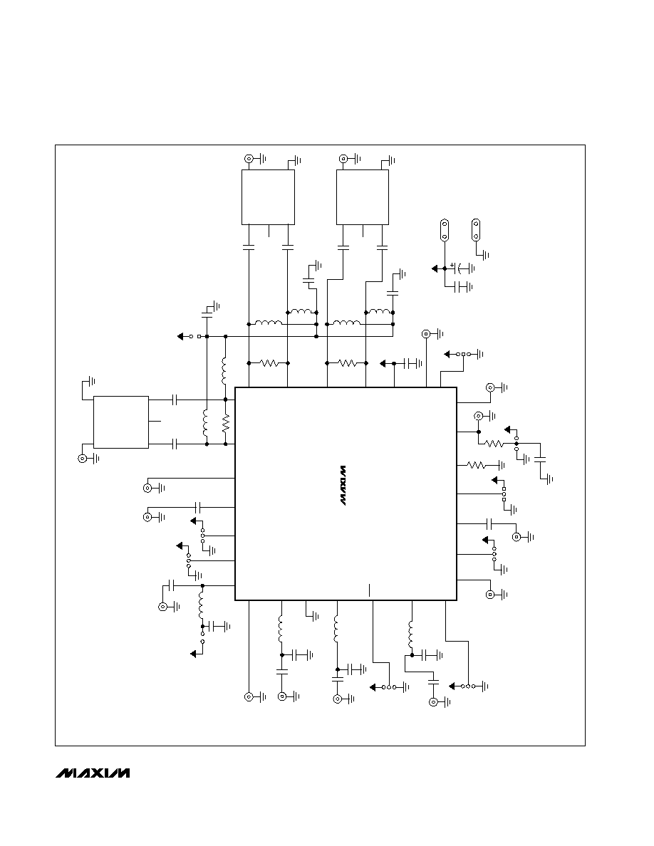
evaluation. Figure 1 shows the schematic. Figures 2
through 7 are component placement guides and PC
board layouts.
Test Equipment Required
This section lists the test equipment recommended to
verify operation of the MAX2530/MAX2531/MAX2538
EV kits. It is intended as a guide only, and some substi-
tutions are possible.
� Two RF signal generators capable of delivering
0dBm of output power up to 2.5GHz (HP 8648C or
equivalent)
� An RF spectrum analyzer capable of covering the
operating frequency range of the devices as well as
a few harmonics (HP 8561E, for example)
� A power supply capable of 50mA at 2.7V to 3.3V
� (Optional) An ammeter for measuring the supply
current
� 50
SMA cables
� (Optional) A network analyzer (HP 8753D, for exam-
ple) to measure small-signal return loss and gain
Connections and Setup
This section provides a step-by-step guide to operating
the EV kits and testing the devices' functions. Do not
turn on DC power or RF signal generators until all con-
nections are made.
Testing the LNA
1) Set the jumpers for the desired mode according to
Table 1 and Table 2.
2) Connect a DC supply (preset to 2.75V) to the V
CC
and GND terminals (through an ammeter, if desired)
on the EV kit.
3) Set the RF generator and spectrum analyzer to oper-
ate at the frequency of 881MHz for cellular,
1960MHz for PCS, or 1575.42MHz for GPS at a
power level of -30dBm.
4) Connect the output of the RF generator to the
respective LNA SMA connector, and connect the
coaxial cable from the LNA output SMA connector to
the spectrum analyzer.
5) Turn on the DC supply and activate the RF generator's
output.
6) The signal that appears on the spectrum analyzer
should have a magnitude of approximately -15dBm
in high-gain mode.
7) (Optional) Another method for determining the gain
is using a network analyzer. This has the advantage
of displaying gain vs. a swept frequency band, in
addition to displaying input and output return loss.
Refer to the user manual of the network analyzer for
setup details.
Testing the Mixer
1) Set the jumpers for the desired mode according to
Table 1 and Table 2.
2) Connect a DC supply (preset to 2.75V) to the V
CC
and GND terminals (through an ammeter, if desired)
on the EV kit.
3) Set one RF generator for an output frequency
of 881MHz for cellular, 1960MHz for PCS, or
1575.42MHz for GPS at a power level of -30dBm.
Connect the output of this generator to the respec-
tive mixer input SMA connector.
Component List (continued)
DESIGNATION
QTY
DESCRIPTION
L5
1
7.5nH �5% inductor (0402)
Coilcraft 0402CS-7N5XJB
R1, R3
2
3.3k
�1% resistors (0402)
R2
1
8.2k
�1% resistor (0402)
R4
1
10k
�5% resistor (0402)
R15
1
20k
�1% resistor (0402)
T1, T2, T3
3
4:1 balun transformers
Toko 617DB-1018
U1
1
MAX2530ETI for MAX2530EVKIT
MAX2531ETI for MAX2531EVKIT
MAX2538ETI for MAX2538EVKIT
Evaluation Kit Selector Guide
TO EVALUATE
USE
MAX2351
MAX2531EVKIT
MAX2354
MAX2530EVKIT
MAX2358
MAX2538EVKIT
MAX2359
MAX2538EVKIT
MAX2530
MAX2530EVKIT
MAX2531
MAX2531EVKIT
MAX2537
MAX2538EVKIT
MAX2538
MAX2538EVKIT

4) Set a second RF generator output frequency
according to Table 3, and connect it to the LO input
port (LO_IN).
5) Connect the coaxial cable from the desired IF port
SMA connector to the spectrum analyzer. See Table
2 for IF port and jumper settings.
6) Set the spectrum analyzer center frequency to
183.6MHz.
7) Turn on the DC supply and activate the RF genera-
tors' outputs.
8) The signal that appears on the spectrum analyzer
should have an amplitude of approximately -17dBm
in high-gain mode.
Layout
A good PC board layout is an essential part of an RF cir-
cuit design. The EV kit PC board can serve as a guide
for laying out a board using the MAX2351/MAX2354/
MAX2358/MAX2359/MAX2530/MAX2531/MAX2537/
MAX2538. Put a decoupling capacitor close to the
device's VCC pin to minimize supply coupling. Proper
grounding of the GND pin is essential. Connect the
GND pin to the ground plane either directly or through
vias as close to the pin as possible. Keep traces carry-
ing RF signals as short as possible to minimize radiation
and insertion loss. Keep the differential mixer output
traces together and of equal length to ensure signal bal-
ance. Solder the entire bottom-side exposed pad evenly
to the board ground plane for proper device operation.
Run the LNA input trace on the top layer of the PC
board to avoid via-induced coupling. Minimize parallel
RF traces to improve coupling loss and isolation. Use
abundant ground vias between RF traces to minimize
undesired coupling.
Evaluate: MAX2351/4/8/9/MAX2530/1/7/8
Quadruple-Mode LNA/Mixer Evaluation Kits
_______________________________________________________________________________________
3
BAND
OPERATING MODE
IF_SEL
G2
G1
MODE
BAND
High gain/high linearity
0 = IF0
1 = IF1
LO
LO
HI
LO
High gain/low linearity
0 = IF0
1 = IF1
LO
LO
LO
LO
Midgain
0 = IF0
1 = IF1
LO
HI
X
LO
Low gain
0 = IF0
1 = IF1
HI
HI
X
LO
Cellular
Ultra-low gain
0 = IF0
1 = IF1
HI
LO
X
LO
High gain/high linearity
0 = IF0
1 = IF1
LO
LO
HI
HI
Low gain
0 = IF0
1 = IF1
HI
HI
X
HI
PCS
Ultra-low gain
0 = IF0
1 = IF1
HI
LO
X
HI
GPS
GPS
X
LO
LO
LO
HI
Table 1. Modes of Operation
X = Don't care.
Evaluate: MAX2351/4/8/9/MAX2530/1/7/8
Quadruple-Mode LNA/Mixer Evaluation Kits
4
_______________________________________________________________________________________
PART
CELL (MHz)
PCS (MHz)
GPS (MHz)
LO GENERATION
MAX2530
1064.6
2143.6
2087.73
--
MAX2531
1064.6
1071.8
1043.865
LO multiplier
MAX2538
2129.2
2143.6
2087.73
LO divider
SUPPLIER
PHONE
FAX
WEBSITE
AVX
843-448-9411
803-626-3123
www.avxcorp.com
Coilcraft
847-639-6400
803-639-1469
www.coilcraft.com
Murata
770-436-1300
770-436-3030
www.murata.com
Taiyo Yuden
800-348-2496
847-925-0899
www.t-yuden.com
Toko
847-297-0070
847-699-7864
www.toko.com
Table 3. LO input (LO_IN) Frequency for Mixer Testing
NAME
FUNCTION
BUF_EN
LO Buffer Enable. On enables the LO buffer output, off disables LO buffer.
G1, G2, MODE, BAND
Set device operating modes according to Table 1.
IF_SEL
Selects IF Port. 0 selects IF0 port, 1 selects IF1 port.
JU1
V
CC
for PCS LNA. Can be used for monitoring the LNA current.
JU2
V
CC
for IF Ports. Can be used for monitoring the mixer current.
PLL_EN
PLL Enable. On enables the PLL drive output, off disables the PLL drive output.
SHDN
Shutdown. On for normal operation, off to shut down the device.
Table 2. Jumper Settings
Component Suppliers
Evaluate: MAX2351/4/8/9/MAX2530/1/7/8
Quadruple-Mode LNA/Mixer Evaluation Kits
_______________________________________________________________________________________
5
MAX2530
MAX2531
MAX2538
PLNA_OUT
CLNA_OUT
PLNA_IN
GND
BAND
IF_SEL
PMIX_IN
CMIX_IN
IF1-
IF1+
VCC
L2
3.3nH
21
C16
100pF
C3
8.2pF
PLNA_OUT
C29
6800pF
PMIX_IN
28
1
2
3
27
26
25
CMIX_IN
IF1
24
23
22
BAND
VCC
IF_SEL
VCC
C7
1000pF
R3
3.3k
L8
120nH
L1
120nH
C2
2.7pF
C1
2.7pF
12
3
46
CLNA_OUT
PLNA_IN
L4
1.0nH
C25
6800pF
C15
1.2pF
CLNA_IN
4
GLNA_IN
GLNA_OUT
GLNA_OUT
6
G1
7
8
G2
9
5
CLNA_IN
GMIX_IN
GLNA_IN
L5
7.5nH
C26
6800pF
C17
2.4pF
VCC
SHDN
VCC
G1
SHDN
L14
3.3nH
C6
1.8pF
C27
6800pF
LO_IN
LO_OUT
G2
VCC
MODE
11
BIAS
12
PLL
LO_IN
BUFFEN
13
14
15
LO_OUT
16
V
CC
17
IFO+
18
IFO-
19
GMIX_IN
10
MODE
VCC
VCC
C28
6800pF
R15
20k
R4
10k
C24
1000pF
PLL_EN
PLL_OUT
VCC
VCC
VCC
BUF_EN
C12
100pF
C11
1000nF
C4
10
�
F
VCC
GND
C13
1000pF
L13
120nH
L3
120nH
R1
3.3k
1
2
4:1
BALUN
3
6
4
GPS_IF
C14
2.7pF
C5
2.7pF
GIF+
20
GIF-
21
C8
1000pF
L7
120nH
L6
120nH
R2
8.2k
C10
2.7pF
C9
2.7pF
T2
1
2
4:1
BALUN
3
6
4
IFO
T1
4:1
BALUN
T3
VCC
JU2
U1
JU1
Figure 1. MAX2530/MAX2531/MAX2538 EV Kits Schematic