 | ÐлекÑÑоннÑй компоненÑ: MAX2609 | СкаÑаÑÑ:  PDF PDF  ZIP ZIP |
MAX2605-9 DS
General Description
The MAX2605MAX2609 are compact, high-performance
intermediate-frequency (IF) voltage-controlled oscillators
(VCOs) designed specifically for demanding portable
wireless communication systems. They combine monolith-
ic construction with low-noise, low-power operation in a
tiny 6-pin SOT23 package.
These low-noise VCOs feature an on-chip varactor and
feedback capacitors that eliminate the need for external
tuning elements, making the MAX2605MAX2609 ideal
for portable systems. Only an external inductor is
required to set the oscillation frequency. In addition, an
integrated differential output buffer is provided for dri-
ving a mixer or prescaler. The buffer output is capable
of supplying up to -8dBm (differential) with a simple
power match. It also provides isolation from load
impedance variations.
The MAX2605MAX2609 operate from a single +2.7V to
+5.5V supply and offer low current consumption. These IF
oscillators can cover the 45MHz to 650MHz frequency
range.
Applications
Cellular and PCS Mobile Phones
2.4GHz ISM Band
902MHz to 928MHz ISM Band
Land Mobile Radio
GPS Receivers
General-Purpose IF Oscillators
Features
o Small Size
o Integrated Varactor for Tuning
o Low Phase Noise
o Wide Application Frequency Range
o Differential or Single-Ended Outputs
o Single +2.7V to +5.5V Supply
o Ultra-Small SOT23-6 Package
o On-Chip Temperature-Stable Bias
o Low-Current Operation
MAX2605MAX2609
45MHz to 650MHz, Integrated IF
VCOs with Differential Output
________________________________________________________________ Maxim Integrated Products
1
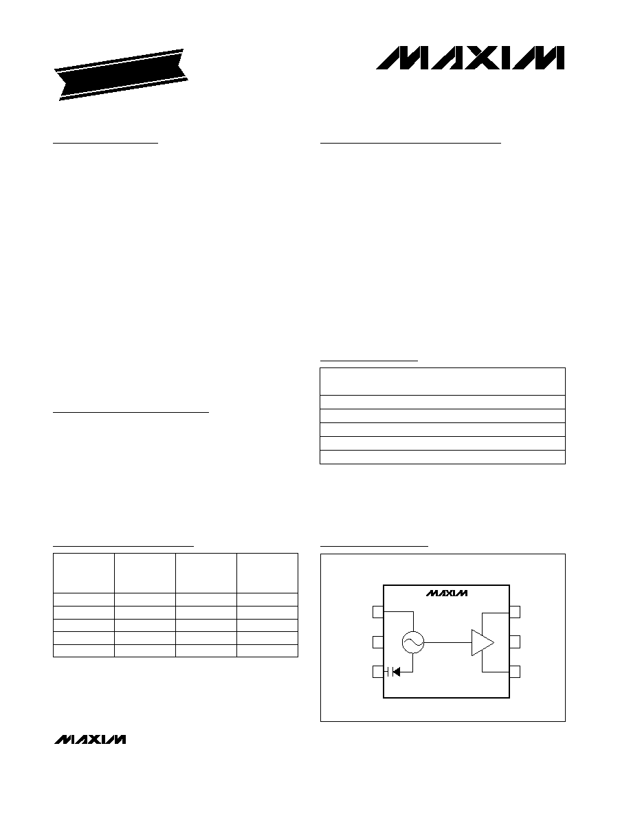
GND
OUT-
TUNE
1
6
OUT+
5
V
CC
IND
MAX2605
MAX2606
MAX2607
MAX2608
MAX2609
SOT23-6
TOP VIEW
2
3
4
19-1673; Rev 0a; 4/02
EVALUATION KIT MANUAL
AVAILABLE
Pin Configuration/
Functional Diagram
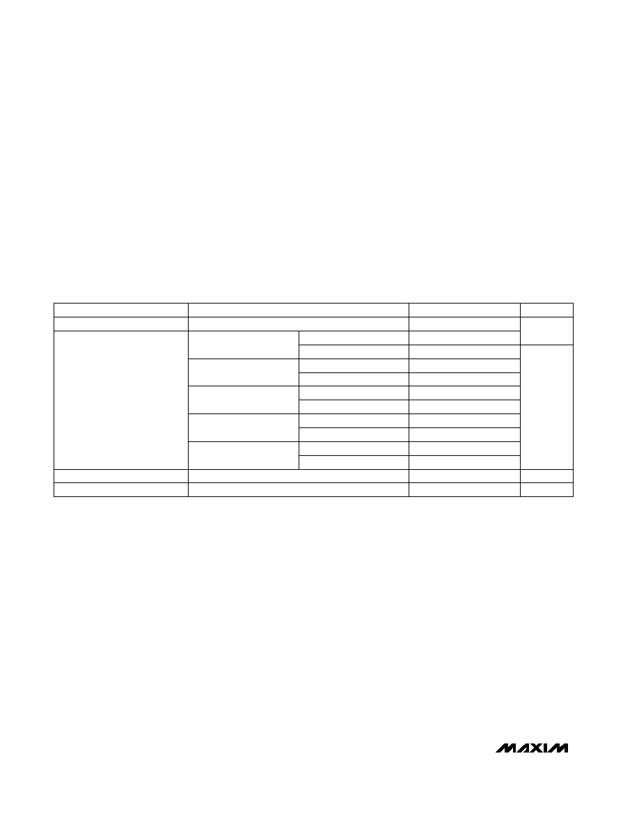
Ordering Information
PART
MAX2605
MAX2606
MAX2607
150 to 300
70 to 150
45 to 70
FREQUENCY
RANGE
(MHz)
SUPPLY
CURRENT
(mA)
1.9
2.1
2.1
MAX2608
300 to 500
2.7
PHASE
NOISE
(dBc/Hz)
-117
-112
-107
-100
MAX2609
500 to 650
3.6
-93
Selector Guide
AABE
6 SOT23-6
-40°C to +85°C
MAX2608EUT-T
AABD
AABC
AABB
TOP
MARK
6 SOT23-6
6 SOT23-6
6 SOT23-6
PIN-
PACKAGE
TEMP. RANGE
-40°C to +85°C
-40°C to +85°C
-40°C to +85°C
MAX2607EUT-T
MAX2606EUT-T
MAX2605EUT-T
PART
AABF
6 SOT23-6
-40°C to +85°C
MAX2609EUT-T
For pricing, delivery, and ordering information, please contact Maxim/Dallas Direct! at
1-888-629-4642, or visit Maxim's website at www.maxim-ic.com.
MAX2605MAX2609
45MHz to 650MHz, Integrated IF
VCOs with Differential Output
2
_______________________________________________________________________________________
ABSOLUTE MAXIMUM RATINGS
DC ELECTRICAL CHARACTERISTICS
(V
CC
= +2.7V to +5.5V, V
TUNE
= 0.4V to 2.4V, T
A
= -40°C to +85°C, unless otherwise noted. Typical values are at V
CC
= +2.75V,
V
TUNE
= 1.5V, and T
A
= +25°C.) (Note1)
Stresses beyond those listed under "Absolute Maximum Ratings" may cause permanent damage to the device. These are stress ratings only, and functional
operation of the device at these or any other conditions beyond those indicated in the operational sections of the specifications is not implied. Exposure to
absolute maximum rating conditions for extended periods may affect device reliability.
V
CC
to GND ..............................................................-0.3V to +6V
IND to GND ................................................-0.6V to (V
CC
+ 0.3V)
TUNE to GND .............................................-0.3V to (V
CC
+ 0.3V)
OUT+, OUT- to GND ..................................-0.3V to (V
CC
+ 0.6V)
Continuous Power Dissipation (T
A
= +85°C)
6-Pin SOT23 (derate
8.7
mW/°C above +70°C) ...........696mW
Operating Temperature Range ...........................-40°C to +85°C
Junction Temperature ......................................................+150°C
Storage Temperature Range .............................-65°C to +150°C
Lead Temperature (soldering, 10s) .................................+300°C
mA
MAX2609
T
A
= -40°C to +85°C
T
A
= +25°C
7.5
DC Output Current (Note 3)
0.5
1.0
1.5
OUT+ plus OUT-
T
A
= -40°C to +85°C
T
A
= +25°C
T
A
= -40°C to +85°C
T
A
= +25°C
T
A
= -40°C to +85°C
T
A
= +25°C
T
A
= -40°C to +85°C
T
A
= +25°C
PARAMETER
MIN
TYP
MAX
UNITS
3.5
2.1
3.2
3.0
Supply Current (Note 2)
2.1
2.7
2.7
4.4
5.5
3.6
6.8
TUNE Input Current
0.03
nA
Supply Voltage
2.7
5.5
V
1.9
2.6
2.8
CONDITIONS
MAX2607
MAX2606
MAX2608
MAX2605
mA
45MHz to 650MHz, Integrated IF
VCOs with Differential Output
_______________________________________________________________________________________
3
AC ELECTRICAL CHARACTERISTICS
(MAX2605MAX2609 EV kits, V
CC
= +2.7V to +5.5V, V
TUNE
= 0.4V to 2.4V, T
A
= -40°C to +85°C, unless otherwise noted. Typical val-
ues are at V
CC
= +2.75V, V
TUNE
= 1.5V, and T
A
= +25°C.) (Note 1)
MAX2609, Q
L
40
Peak Tuning Gain
14.5
%/V
V
TUNE
= 0.4V to 0.6V step (Note 6)
T
A
= +25°C
-5.0
+3.8
500
650
MAX2609
MAX2608, Q
L
40
MAX2607, Q
L
35
MAX2606, Q
L
35
MAX2605, Q
L
35
-107
dBc/Hz
-100
-93
-117
Phase Noise (Note 8)
-112
f
OFFSET
= 100kHz
-4.7
+3.6
T
A
= +25°C
T
A
= +25°C
T
A
= +25°C
T
A
= +25°C
PARAMETER
MIN
TYP
MAX
UNITS
Guaranteed Frequency Limits
(relative to nominal) (Note 5)
-4.1
+3.2
300
500
-4.4
+3.4
-4.6
+3.6
Oscillator Nominal Frequency
Range (Note 4)
45
70
70
150
150
300
CONDITIONS
MAX2606
MAX2605
MAX2608
MAX2607
MAX2608
MAX2605
MAX2606
MAX2607
Single-Ended Output Power
(Note 7)
-10
dBm
T
A
= -40°C to +85°C
T
A
= -40°C to +85°C
T
A
= -40°C to +85°C
T
A
= -40°C to +85°C
T
A
= -40°C to +85°C
-2.25
+2.25
-2.5
+2.5
-2.75
+2.75
-2.8
+2.8
-3.0
+3.0
MAX2605MAX2609
MAX2609
MHz
%
MAX2605MAX2609
45MHz to 650MHz, Integrated IF
VCOs with Differential Output
4
_______________________________________________________________________________________
AC ELECTRICAL CHARACTERISTICS (continued)
(MAX2605MAX2609 EV kits, V
CC
= +2.7V to +5.5V, V
TUNE
= 0.4V to 2.4V, T
A
= -40°C to +85°C, unless otherwise noted. Typical val-
ues are at V
CC
= +2.75V, V
TUNE
= 1.5V, and T
A
= +25°C.) (Note 1)
Note 1: Production tested at T
A
= +25°C. Maximum and minimum over temperature limits are guaranteed by design and
characterization.
Note 2: Supply current is measured while the part is oscillating and inductor Q
Q
MIN
. For MAX2605/MAX2606/MAX2607, Q
MIN
= 35;
for MAX2608/MAX2609, Q
MIN
= 40.
Note 3: The DC output current is the total available output signal current.
Note 4: Application range of the part is achieved using external inductance as specified in Figures 1-5 and shown in Figure 6. The inter-
nal varactors support center frequencies of 45MHz to 650MHz. The center frequency is defined by the value of the external
inductor element, L
F
. The application frequency limits are guaranteed by design and characterization.
Note 5: The guaranteed (tested) limits
MIN
and
MAX
are measured at V
TUNE
= 0.4V and V
TUNE
= 2.4V, respectively. Passing
requirements are:
MIN
at V
TUNE
= 0.4 and
MAX
at V
TUNE
= 2.4V. The nominal frequency of oscillation is defined by
the inductor.
Note 6: Describes peak tuning gain, which occurs at V
TUNE
= 0.4V.
Note 7: Measurement at OUT+ or OUT- matched for optimum power transfer into 50
load near the center of the operating frequency
range.
Note 8: The phase-noise specifications listed apply to the typical operating circuit shown in Figure 6. Apply over the entire operating
frequency range of the MAX2605MAX2609.
Note 9: Supply pushing is measured with V
CC
stepped from +2.7V to +3.2V.
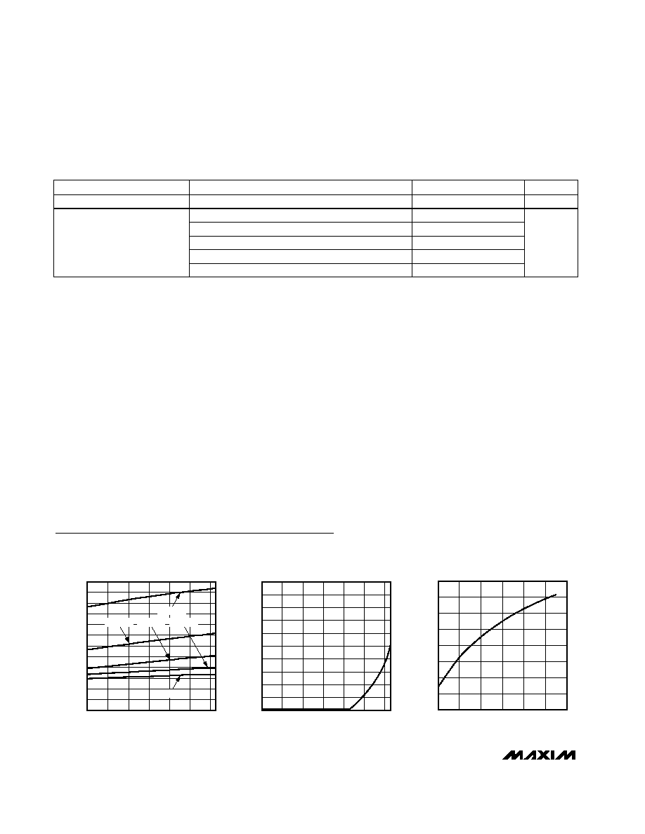
1.0
1.5
2.0
3.0
2.5
3.5
4.0
-40
0
-20
20
40
60
80
SUPPLY CURRENT
vs. TEMPERATURE
MAX2605/9-01
TEMPERATURE (°C)
SUPPLY CURRENT (mA)
MAX2609
MAX2605
MAX2606
MAX2607
MAX2608
0
0.02
0.06
0.04
0.08
0.10
-40
0
-20
20
40
60
80
TUNE INPUT LEAKAGE CURRENT
vs. TEMPERATURE
MAX2605/9-02
TEMPERATURE (
°C)
LEAKAGE CURRENT (nA)
45
50
55
60
65
0
1.0
0.5
1.5
2.0
2.5
3.0
MAX2605
VCO TUNING CURVE
MAX2605/9-03
V
TUNE
(V)
FREQUENCY (MHz)
Typical Operating Characteristics
(MAX260_ EV kit, V
CC
= +2.75V, V
TUNE
= 1.4V, T
A
= +25°C, unless otherwise noted.)
dBc
Even-Order Harmonics
-30
Differential, R
L
= 50
each side
PARAMETER
MIN
TYP
MAX
UNITS
60
CONDITIONS
MAX2605
120
MAX2606
480
MAX2608
220
MAX2607
Supply Pushing (Note 9)
720
kHz/V
MAX2609
_______________________________________________________________________________________
5
MAX2605MAX2609
45MHz to 650MHz, Integrated IF
VCOs with Differential Output
90
100
110
120
130
0
1.0
0.5
1.5
2.0
2.5
3.0
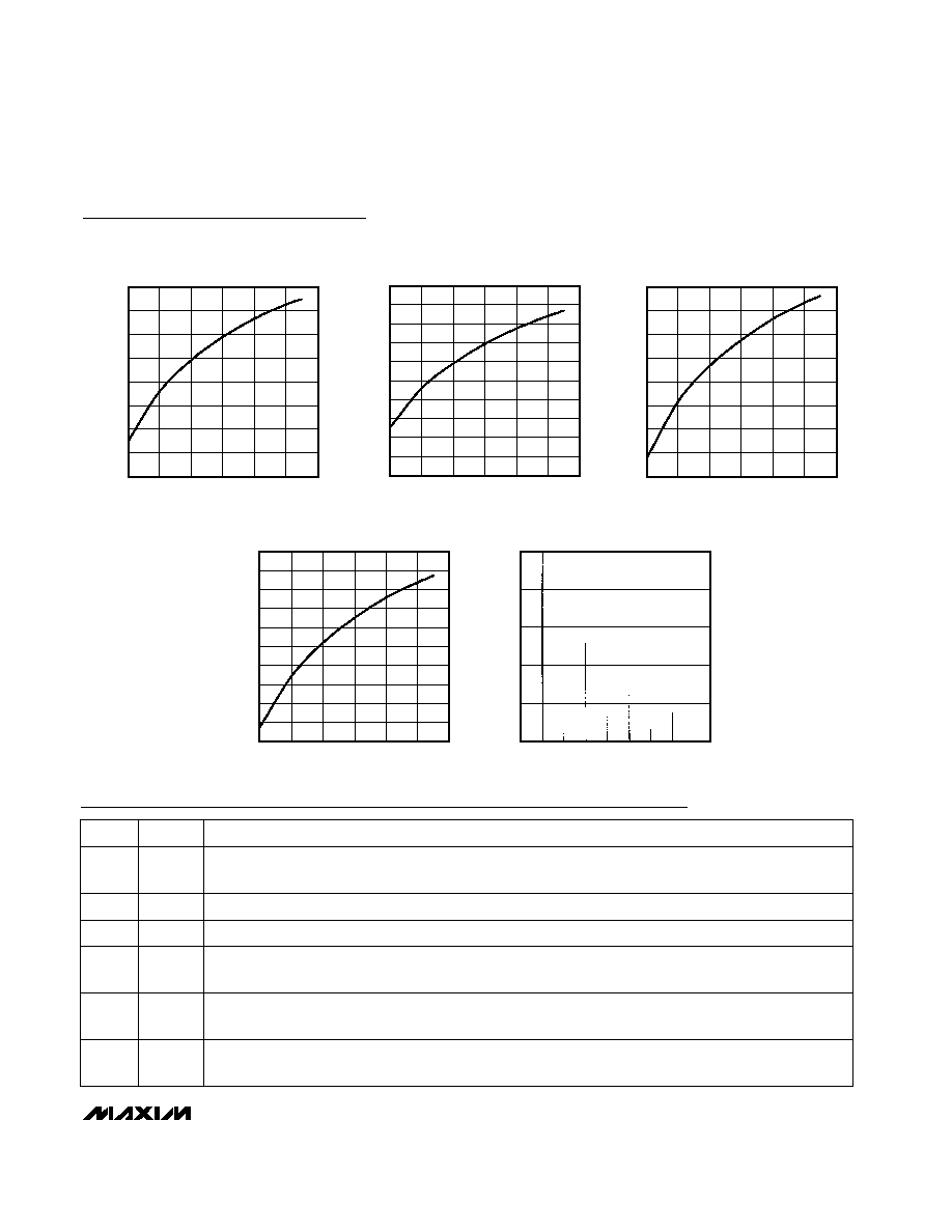
MAX2606
VCO TUNING CURVE
MAX2605/9-04
V
TUNE
(V)
FREQUENCY (MHz)
160
180
200
220
240
260
0
1.0
0.5
1.5
2.0
2.5
3.0
MAX2607
VCO TUNING CURVE
MAX2605/9-05
V
TUNE
(V)
FREQUENCY (MHz)
310
340
370
400
430
0
1.0
0.5
1.5
2.0
2.5
3.0
MAX2608
VCO TUNING CURVE
MAX2605/9-06
V
TUNE
(V)
FREQUENCY (MHz)
480
520
560
600
640
680
0
1.0
0.5
1.5
2.0
2.5
3.0
MAX2609
VCO TUNING CURVE
MAX2605/9-07
V
TUNE
(V)
FREQUENCY (MHz)
-50
-40
-30
-20
-10
0
4f
o
5f
o
2f
o
3f
o
f
o
6f
o
7f
o
MAX2605/9-08
FREQUENCY
(dB)
OUTPUT SPECTRUM
NAME
FUNCTION
1
IND
Tuning Inductor Port. Connect an inductor from IND to GND to set VCO center frequency (see Oscillation
Frequency).
2
GND
Ground. Connect to the ground plane with a low-inductance path.
PIN
3
TUNE
Voltage-Control Input for Frequency Tuning. Input voltage range from +0.4V to +2.4V.
4
OUT-
High-Impedance Open-Collector Output. An external pull-up resistor or inductor to V
CC
is required. Output
power is dependent on external load impedance. OUT- is complementary to OUT+.
6
OUT+
High-Impedance Open-Collector Output. An external pull-up resistor or inductor to V
CC
is required. Output
power is dependent on external load impedance. OUT+ is complementary to OUT-.
5
V
CC
Supply Voltage Connection. Connect an external bypass capacitor to ground for low noise and low spuri-
ous-output content. See Layout Issues for more details.
Pin Description
Typical Operating Characteristics (continued)
(MAX260_ EV kit, V
CC
= +2.75V, V
TUNE
= 1.4V, T
A
= +25°C, unless otherwise noted.)