_______________General Description
The MAX2650 is a low-noise amplifier for use from DC
to microwave frequencies. Operating from a single +5V
supply, it has a flat gain response to 900MHz. The
MAX2650's low noise figure and high drive capability
make it ideal for a variety of transmit, receive, and
buffer applications.
The device is internally biased, eliminating the need for
external bias resistors or inductors. In a typical applica-
tion, the only external components needed are input
and output blocking capacitors and a V
CC
bypass
capacitor.
The MAX2650 comes in a 4-pin SOT143 package,
requiring minimal board space.
________________________Applications
Wireless Local Loop
Global Positioning Systems (GPS)
ISM Radios
Special Mobile Radios
Wireless Local-Area Networks
Cellular Base Stations
Set-Top Boxes
____________________________Features
o
Internally Biased
o
High Gain: 18.3dB at 900MHz
o
3.9dB Noise Figure
o
Single +4.5V to +5.5V Operation
o
-1dBm Output 1dB Compression Power
o
Low-Cost Silicon Bipolar Design
o
Ultra-Small SOT143 Package
MAX2650
DC-to-Microwave,
+5V Low-Noise Amplifier
________________________________________________________________
Maxim Integrated Products
1
__________________Pin Configuration
V
CC
C
BYP
C
BLOCK
GND
OUT
OUT
V
CC
IN
C
BLOCK
IN
MAX2650
OUT
V
CC
GND
3
4
2
1
IN
SOT143
TOP VIEW
MAX2650
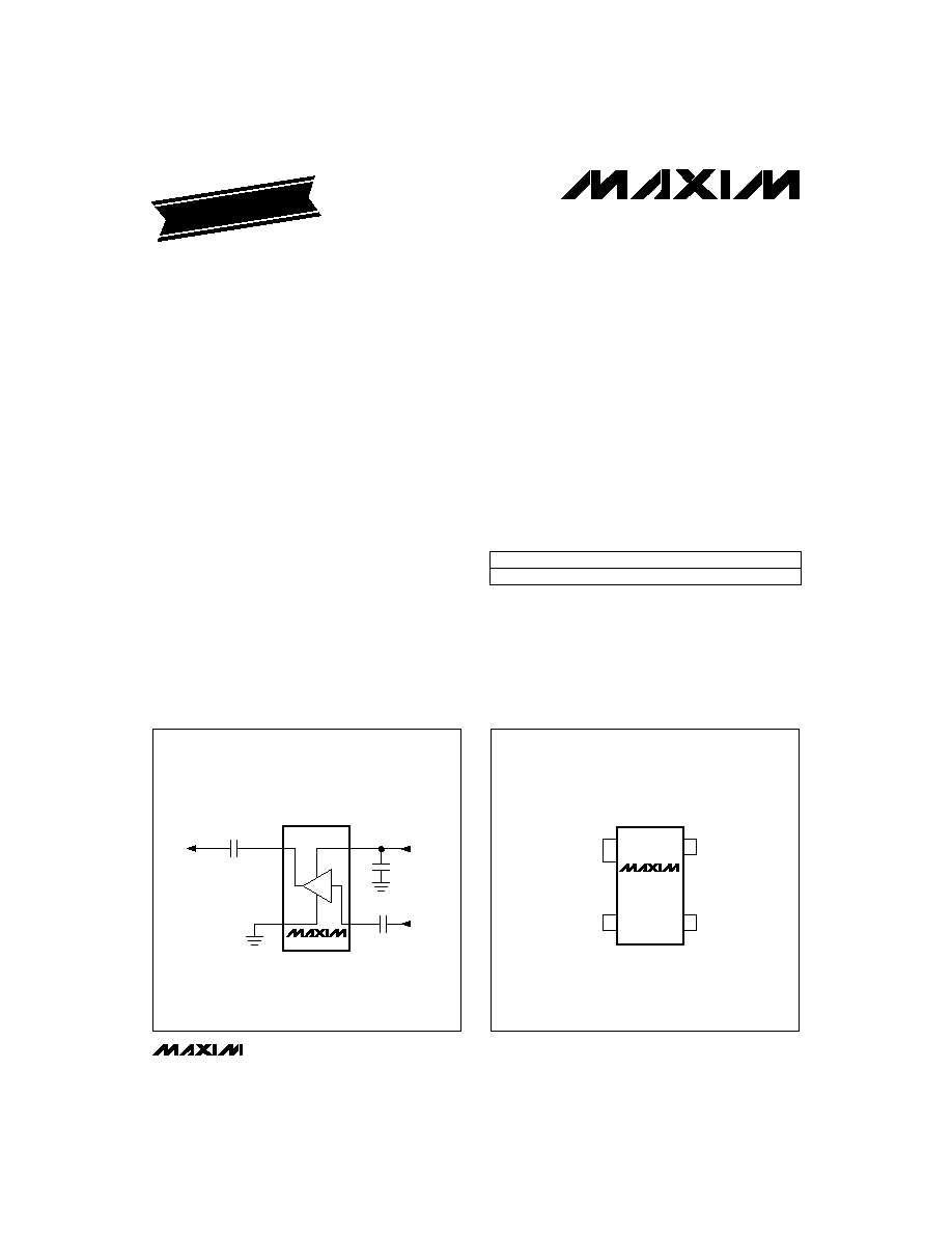
__________Typical Operating Circuit
19-1135; Rev 0; 9/96
PART
MAX2650EUS-T
-40�C to +85�C
TEMP. RANGE
PIN-PACKAGE
4 SOT143
EVALUATION PCB
AVAILABLE
______________Ordering Information
For free samples & the latest literature: http://www.maxim-ic.com, or phone 1-800-998-8800
MAX2650
DC-to-Microwave, +5V Low-Noise Amplifier
2
_______________________________________________________________________________________
ABSOLUTE MAXIMUM RATINGS
ELECTRICAL CHARACTERISTICS
(V
CC
= +5.0V, Z
0
= 50
, f
IN
= 900MHz, T
A
= +25�C, unless otherwise noted.)
Stresses beyond those listed under "Absolute Maximum Ratings" may cause permanent damage to the device. These are stress ratings only, and functional
operation of the device at these or any other conditions beyond those indicated in the operational sections of the specifications is not implied. Exposure to
absolute maximum rating conditions for extended periods may affect device reliability.
Note 1:
Parts are designed to operate over specified temperature range. Specifications are production tested and guaranteed
at +25�C.
V
CC
to GND ..............................................................-0.3V to +8V
Input Power ....................................................................+13dBm
Continuous Power Dissipation (T
A
= +70�C)
SOT143-4 (derate 4mW/�C above +70�C)...................320mW
Operating Temperature Range ...........................-40�C to +85�C
Junction Temperature ......................................................+150�C
Storage Temperature Range .............................-65�C to +150�C
Lead Temperature (soldering, 10sec) .............................+300�C
(Note 1)
f
IN
= 800MHz to 1000MHz
f
IN
= 100MHz to 1000MHz
CONDITIONS
dB
16.5
18.3
21
Power Gain
�C
-40
85
Operating Temperature Range
15.5
17.7
20.0
V
4.5
5.5
Supply Voltage
ps
300
Group Delay
1.3:1
Maximum Output Voltage Standing-Wave Ratio
dBm
-1
Output 1dB Compression Point
dBm
10
Output IP3
dB
3.9
Noise Figure
1.5:1
Maximum Input Voltage Standing-Wave Ratio
UNITS
MIN
TYP
MAX
PARAMETER
T
A
= T
MIN
to T
MAX
13.0
17.7
22.0
V
CC
= 4.5V to 5.5V
mA
11.0
17.7
24.0
Supply Current

MAX2650
DC-to-Microwave, +5V Low-Noise Amplifier
_______________________________________________________________________________________
3
40
0
4.0
6.0
SUPPLY CURRENT
vs. SUPPLY VOLTAGE
10
30
MAX2650-01
V
CC
(V)
I
CC
(mA)
20
5.5
5.0
4.5
+85�C
-40�C
+25�C
5
-5
0.1
0.3
1.5
OUTPUT 1dB COMPRESSION
POINT vs. FREQUENCY
-1
-3
3
MAX2650-02
FREQUENCY (GHz)
P
-1
(dBm)
1
1.3
1.1
0.9
0.7
0.5
-40�C
+25�C
+85�C
+5
-5
0.1
0.3
1.5
OUTPUT 1dB COMPRESSION
POINT vs. FREQUENCY
-1
-3
+3
MAX2650-03
FREQUENCY (GHz)
P
-1
(dBm)
+1
1.3
1.1
0.9
0.7
0.5
5.5V
4.5V
5.0V
25
0
0.1
0.3
1.5
GAIN vs. FREQUENCY
10
5
20
MAX2650-04
FREQUENCY (GHz)
GAIN (dB)
15
1.3
1.1
0.9
0.7
0.5
+85�C
-40�C
+25�C
3.5:1
1.0:1
0.1
0.3
1.5
VOLTAGE STANDING-WAVE RATIO
vs. FREQUENCY
2.0:1
OUT
IN
1.5:1
3.0:1
MAX2650-06
FREQUENCY (GHz)
VSWR
2.5:1
1.3
1.1
0.9
0.7
0.5
25
0
0.1
0.3
1.5
GAIN vs. FREQUENCY
10
5
20
MAX2650-05
FREQUENCY (GHz)
GAIN (dB)
15
1.3
1.1
0.9
0.7
0.5
5.5V
4.5V
5.0V
5
0
0.1
0.3
1.5
NOISE FIGURE vs. FREQUENCY
2
+85�C
-40�C
1
4
MAX2650-07
FREQUENCY (GHz)
NOISE FIGURE (dB)
3
1.3
1.1
0.9
0.7
0.5
+25�C
__________________________________________Typical Operating Characteristics
(V
CC
= 5.0V, Z
0
= 50
, f
IN
= 900MHz, T
A
= +25�C, unless otherwise noted.)

MAX2650
DC-to-Microwave, +5V Low-Noise Amplifier
4
_______________________________________________________________________________________
Table 1. Typical Scattering Parameters
(V
CC
= +5V, Z
0
= 50
, T
A
= +25�C.)
0.19
0.20
0.20
0.18
0.18
0.17
0.16
0.16
0.14
0.16
0.17
0.17
S11
(mag)
-86
-66
-54
-39
-26
-17
-7
0
8
9
-6
-3
S11
(ang)
15.7
17.4
18.0
18.6
19.0
19.3
19.5
19.6
19.7
19.7
19.8
19.8
S21
(dB)
6.10
7.40
7.92
8.46
8.93
9.21
9.43
9.52
9.70
9.69
9.72
9.76
S21
(mag)
51
73
84
95
107
119
129
140
151
161
172
177
S21
(ang)
-26.9
-28.7
-29.5
-31.1
-31.7
-32.3
-33.2
-33.8
1.20
-35.0
-35.8
-36.7
0.20
-37.8
S12
(dB)
0.045
0.10
0.037
0.033
0.05
0.028
0.026
0.024
0.022
1.00
0.020
0.018
0.016
0.90
0.015
0.013
S12
(mag)
0.80
52
50
48
0.70
44
41
37
0.30
34
32
28
0.40
23
14
8
0.50
S12
(ang)
0.05
0.10
0.60
0.13
0.17
0.21
FREQUENCY
(GHz)
0.25
0.28
0.32
0.35
0.37
0.39
0.42
S22
(mag)
-49
-76
-71
-62
-53
-43
-34
-26
-19
-13
-6
-5
S22
(ang)
1.88
1.88
1.91
2.10
2.09
2.12
2.24
2.31
2.54
2.70
2.92
3.18
K
1.40
0.16
-86
13.4
4.69
31
-25.5
0.053
51
0.12
-12
2.03
1.60
0.15
-66
10.6
3.40
14
-24.4
0.060
44
0.24
-17
2.32
1.80
0.22
-40
7.4
2.35
5
-24.4
0.060
32
0.35
-27
3.01
2.00
0.33
-36
4.6
1.70
4
-25.3
0.055
22
0.43
-33
3.97
2.20
0.41
-38
3.1
1.43
6
-26.5
0.047
21
0.46
-33
4.85
2.40
0.44
-37
2.5
1.34
6
-28.6
0.037
22
0.49
-29
6.26
2.50
0.44
-37
2.3
1.30
4
-29.5
0.034
22
0.49
-25
7.05
______________________________________________________________Pin Description
NAME
FUNCTION
1
IN
Amplifier Input. Use a series blocking capacitor with less than 3
reactance at your lowest operating
frequency.
2
GND
Ground Connection. For optimum performance, provide a low-inductance connection to the ground
plane.
PIN
3
OUT
Amplifier Output. Use a series blocking capacitor with less than 3
reactance at your lowest operat-
ing frequency.
4
V
CC
Supply Connection. Bypass directly at the package pin. The value of the bypass capacitor is deter-
mined by the lowest operating frequency and is typically the same as the blocking capacitor value.
For long V
CC
lines, additional bypassing may be necessary.

_______________Detailed Description
The MAX2650 is a broadband amplifier with flat gain
and 50
input and output ports. Its small size and inter-
nal bias circuitry make it ideal for applications where
board space is limited.
__________Applications Information
External Components
As shown in the
Typical Operating Circuit, the
MAX2650 is easy to use. Input and output series
capacitors may be necessary to block DC bias volt-
ages (generated by the MAX2650) from interacting with
adjacent circuitry. These capacitors must be large
enough to contribute negligible reactance in a 50
sys-
tem at the minimum operating frequency. Use the fol-
lowing equation to calculate their minimum value:
where f (in MHz) is the minimum operating frequency.
The V
CC
pin must be RF bypassed for correct opera-
tion. To accomplish this, connect a capacitor between
the V
CC
pin and ground, as close to the package as is
practical. Use the same equation given above (for DC
blocking capacitor values) to calculate the minimum
capacitor value. If there are long V
CC
lines on the PC
board, additional bypassing may be necessary. This
may be done further away from the package, at your
discretion.
Proper grounding of the GND pin is essential. If the PC
board uses a topside RF ground, the GND pin should
connect directly to it. For a board where the ground
plane is not on the component side, the best technique
is to connect the GND pin to it through multiple plated
through-holes.
PC Board Layout Example
An example PC board layout is given in Figure 1. It
uses FR-4 with 31mil layer thickness between the RF
lines and the ground plane. The board satisfies all the
above requirements.
C
BLOCK
=
53,000
f
(pF)
MAX2650
DC-to-Microwave, +5V Low-Noise Amplifier
_______________________________________________________________________________________
5
Figure 1. Example PC Board Layout
EXPANDED VIEW
RF IN
RF OUT
V
CC
MAX2650