 | –≠–Ľ–Ķ–ļ—ā—Ä–ĺ–Ĺ–Ĺ—č–Ļ –ļ–ĺ–ľ–Ņ–ĺ–Ĺ–Ķ–Ĺ—ā: MAX2750 | –°–ļ–į—á–į—ā—Ć:  PDF PDF  ZIP ZIP |
General Description
The MAX2750/MAX2751/MAX2752 are self-contained volt-
age-controlled oscillators (VCOs) intended for use in the
2.4GHz to 2.5GHz ISM band. Each IC combines a fully
integrated oscillator and output buffer in a miniature 8-pin
ĶMAX package.
The inductor and varactor elements of the tank are inte-
grated on-chip, greatly simplifying application of the part.
The only required external components are a couple of
supply bypass capacitors. The IC provides direct connec-
tion to the VCO tuning voltage input and the VCO buffer
output. The tuning voltage input range is +0.4V to +2.4V,
and the oscillator frequency tuning range is factory adjust-
ed to provide guaranteed limits. The output signal is
buffered by an amplifier stage (internally matched to 50
)
to provide higher output power and isolate the device from
load impedance variations.
The MAX2750/MAX2751/MAX2752 operate over a +2.7V
to +5.5V supply voltage range. Internal regulation of the
oscillator supply voltage eliminates the need for an exter-
nal LDO regulator for the VCO. The IC also provides a dig-
itally controlled shutdown mode to permit implementation
of sophisticated power-supply management. In shutdown,
the supply current is reduced to less than 1ĶA.
________________________Applications
802.11b DSSS WLAN
802.11 FHSS WLAN
Home RF
2.4GHz Bluetooth ISM Proprietary Radio
Features
o Guaranteed Frequency Tuning Range
MAX2750: 2400MHz to 2500MHz (Zero IF)
MAX2751: 2120MHz to 2260MHz
(240MHz to 280MHz IF)
MAX2752: 2025MHz to 2165MHz
(335MHz to 375MHz IF)
o On-Chip Tank Circuit
o Internally Matched Output Buffer Amplifier
o Low-Current Shutdown Mode
o +2.7V to +5.5V Supply Voltage Range
o Miniature 8-Pin ĶMAX Package
MAX2750/MAX2751/MAX2752
2.4GHz Monolithic
Voltage-Controlled Oscillators
________________________________________________________________ Maxim Integrated Products
1
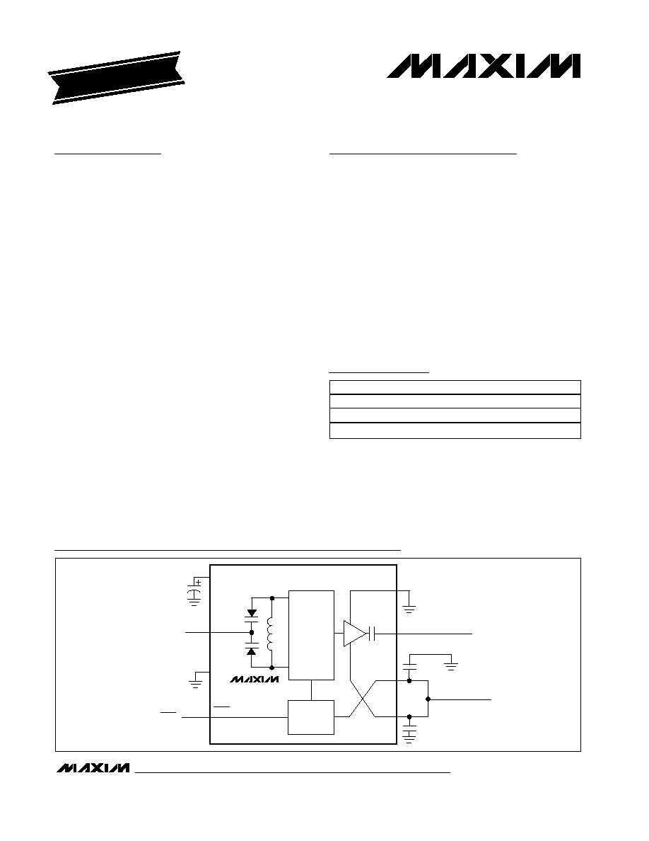
OSCILLATOR
CORE
BIAS
TUNE
TUNE
BYP
SHDN
GND
OUT
V
CC1
V
CC
V
CC2
GND
SHDN
OUT TO MIXER/
SYNTHESIZER
MAX2750
MAX2751
MAX2752
Typical Operating Circuit
19-1825; Rev 0; 10/00
EVALUATION KIT MANUAL
FOLLOWS DATA SHEET
Ordering Information
For price, delivery, and to place orders, please contact Maxim Distribution at 1-888-629-4642,
or visit Maxim's website at www.maxim-ic.com.
PART
TEMP. RANGE
PIN-PACKAGE
MAX2750EUA
-40
įC to +85įC
8 ĶMAX
MAX2751EUA
-40
įC to +85įC
8 ĶMAX
MAX2752EUA
-40
įC to +85įC
8 ĶMAX
Pin Configuration appears at end of data sheet.
ABSOLUTE MAXIMUM RATINGS
MAX2750/MAX2751/MAX2752
2.4GHz Monolithic
Voltage-Controlled Oscillators
2
_______________________________________________________________________________________
DC ELECTRICAL CHARACTERISTICS
(V
CC
= +2.7V to +5.5V, V
TUNE
= +0.4V to +2.4V, V
SHDN
+2V, OUT = connected to 50 load, T
A
= -40įC to +85įC. Typical values
are at V
CC
= +3.0V, T
A
= +25įC, unless otherwise noted.) (Note 1)
AC ELECTRICAL CHARACTERISTICS
(MAX2750/MAX2751/MAX2752 EV kit, V
CC
= +2.7V to +5.5V, V
TUNE
= +0.4V to +2.4V, V
SHDN
+2V, OUT = connected to 50 load,
T
A
= +25įC. Typical values are at V
CC
= +3.0V, unless otherwise noted.)
Stresses beyond those listed under "Absolute Maximum Ratings" may cause permanent damage to the device. These are stress ratings only, and functional
operation of the device at these or any other conditions beyond those indicated in the operational sections of the specifications is not implied. Exposure to
absolute maximum rating conditions for extended periods may affect device reliability.
V
CC
to GND ..............................................................-0.3V to +6V
TUNE, SHDN, BYP, OUT to GND ...............-0.3V to (V
CC
+ 0.3V)
Continuous Power Dissipation (T
A
= +70įC)
8-Pin ĶMAX (derate 5.7mW/įC above T
A
= +70įC).....457mW
Operating Temperature Range ...........................-40įC to +85įC
Junction Temperature ......................................................+150įC
Storage Temperature Range .............................-65įC to +150įC
Lead Temperature (soldering, 10s) .................................+300įC
PARAMETER
CONDITIONS
MIN
TYP
MAX
UNITS
Supply Voltage
2.7
5.5
V
T
A
= +25
o
C
11.3
14.4
MAX2750
T
A
= -40
o
C to +85
o
C
14.1
17.0
T
A
= +25
o
C
9.7
12.1
MAX2751
T
A
= -40
o
C to +85
o
C
12.7
15.9
T
A
= +25
o
C
10
12.1
Supply Current
MAX2752
T
A
= -40
o
C to +85
o
C
12.8
15.2
mA
Shutdown Supply Current
0.2
1
ĶA
SHDN Input Voltage Low
0.6
V
SHDN Input Voltage High
2.0
V
SHDN Input Current Low
V
SHDN
0.6V
-2
2
ĶA
SHDN Input Current High
V
SHDN
2.0V
-2
2
ĶA
TUNE Input Current
0.4
V
TUNE
2.4V
0.02
nA
PARAMETER
CONDITIONS
MIN
TYP
MAX
UNITS
MAX2750
2400
2500
MHz
MAX2751
2120
2260
MHz
Oscillator Guaranteed
Frequency Limits (Note1)
V
TUNE
= +0.4V to +2.4V,
T
A
= -40
o
C to +85
o
C
MAX2752
2025
2165
MHz
f
OFFSET
= 4MHz
-125
dBc/Hz
Phase Noise
Noise floor
-151
dBm/Hz
f
OSC
= 2400MHz, +3V
140
MAX2750
f
OSC
= 2500MHz, +3V
90
f
OSC
= 2120MHz, +3V
175
MAX2751
f
OSC
= 2260MHz, +3V
110
f
OSC
= 2025MHz, +3V
170
Tuning Gain (Note 2)
MAX2752
f
OSC
= 2165MHz, +3V
105
MHz/V
Output Power
-3
dBm
Return Loss
12
dB
Harmonics
-30
dBc

MAX2750/MAX2751/MAX2752
2.4GHz Monolithic
Voltage-Controlled Oscillators
_______________________________________________________________________________________
3
Note 1: Specifications are production tested at T
A
= +25
įC. Limits over temperature are guaranteed by design and characterization.
Note 2: Tuning gain is measured at the oscillator's guaranteed frequency limits.
Note 3: Turn-on time to within 3dB of final output power
Note 4: Turn-off time to output power of -10dBm.
AC ELECTRICAL CHARACTERISTICS (continued)
(MAX2750/MAX2751/MAX2752 EV kit, V
CC
= +2.7V to +5.5V, V
TUNE
= +0.4V to +2.4V, V
SHDN
+2V, OUT = connected to 50 load,
T
A
= +25įC. Typical values are at V
CC
= +3.0V, unless otherwise noted.)
PARAMETER
CONDITIONS
MIN
TYP
MAX
UNITS
Load Pulling
VSWR = 2:1, all phases
4
MHzp-p
Supply Pushing
V
CC
stepped: +3.3V to +2.8V
1.3
MHz/V
Oscillator Turn-On Time (Note 3)
Exiting shutdown
8
Ķs
Oscillator Turn-Off Time (Note 4)
Entering shutdown
5
Ķs
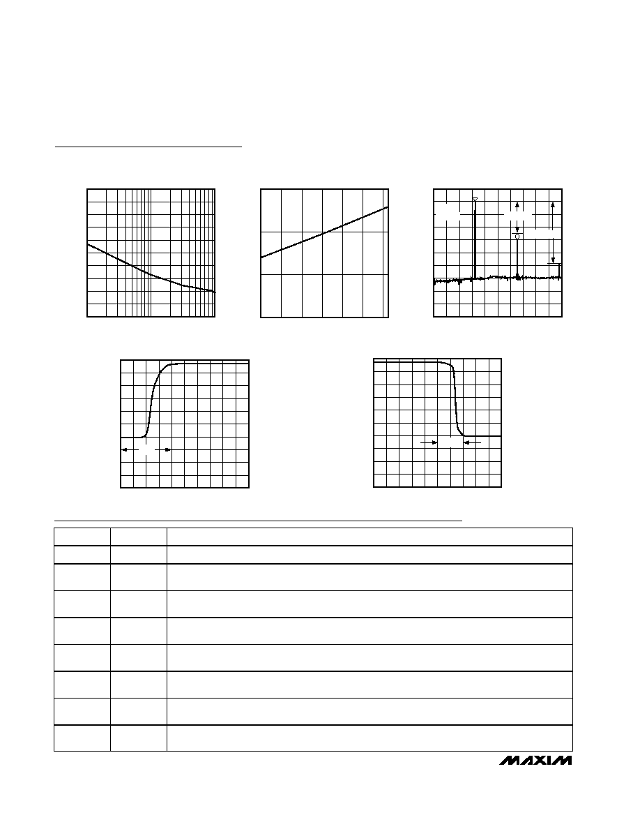
MAX2750/51/52 toc01
7
8
10
9
13
14
12
11
15
SUPPLY CURRENT (mA)
-40
0
20
-20
40
60
80
TEMPERATURE (
įC)
MAX2750/MAX2751/MAX2752
SUPPLY CURRENT vs. TEMPERATURE
MAX2750
MAX2752
MAX2751
0
0.1
0.3
0.2
0.4
0.5
-40
0
-20
20
40
60
80
MAX2750/51/52 toc02
TEMPERATURE (
įC)
SHUTDOWN CURRENT (
Ķ
A)
MAX2750/MAX2751/MAX2752
SHUTDOWN CURRENT vs. TEMPERATURE
MAX2750/51/52 toc03
0
0.2
0.4
0.8
0.6
1.0
TUNE INPUT CURRENT (nA)
-40
0
20
-20
40
60
80
TEMPERATURE (
įC)
MAX2750/MAX2751/MAX2752
TUNING CURRENT vs. TEMPERATURE
2200
2300
2400
2500
2600
0
1.0
0.5
1.5
2.0
2.5
3.0
MAX2750/51/52 toc04
V
TUNE
(V)
FREQUENCY (MHz)
MAX2750
VCO TUNING CURVE
T
A
= +85
įC
T
A
= +25
įC
T
A
= -40
įC
1850
1950
2050
2150
2250
2350
0
0.5
1.0
1.5
2.0
2.5
3.0
MAX2750/51/52 toc05
V
TUNE
(V)
FREQUENCY (MHz)
MAX2751
VCO TUNING CURVE
T
A
= +85
įC
T
A
= +25
įC
T
A
= -40
įC
1850
1950
2050
2150
2250
2350
0
0.5
1.0
1.5
2.0
2.5
3.0
MAX2750/51/52 toc06
V
TUNE
(V)
FREQUENCY (MHz)
MAX2752
VCO TUNING CURVE
T
A
= +85
įC
T
A
= +25
įC
T
A
= -40
įC
Typical Operating Characteristics
(Circuit of Figure 1, V
CC
= +3.0V, V
TUNE
= +0.4V to +2.4V, V
SHDN
2V, T
A
= +25įC, unless otherwise noted.)
MAX2750/MAX2751/MAX2752
2.4GHz Monolithic
Voltage-Controlled Oscillators
4
_______________________________________________________________________________________
Pin Description
0.1
1
10
PHASE NOISE
MAX2750/51/52 toc07
OFFSET FREQUENCY (MHz)
PHASE NOISE (dBc/Hz)
-150
-130
-140
-110
-120
-90
-100
-80
-60
-70
-50
MAX2750/51/52 toc08
TEMPERATURE (
įC)
OUTPUT POWER (dBm)
-5
-4
-3
-2
-40
0
-20
20
40
60
80
MAX2751
OUTPUT POWER vs. TEMPERATURE
MAX2750/51/52 toc09
O
3
O
OUTPUT POWER (dBm)
FREQUENCY
= 48dBc
MKR
-30.00dB
= 30dBc
NORMALIZED HARMONIC
OUTPUT SPECTRUM
2
O
Typical Operating Characteristics (continued)
(Circuit of Figure 1, V
CC
= +3.0V, V
TUNE
= +0.4V to +2.4V, V
SHDN
2V, T
A
= +25įC, unless otherwise noted.)
-100
-80
-90
-60
-70
-40
-50
-30
-10
-20
0
0
4
6
8
2
10 12 14
18
16
20
OSCILLATOR TURN-ON TIME
MAX2750/51/52 toc10
TIME (
Ķs)
OUTPUT POWER (dBm)
8
Ķs
-100
-80
-90
-60
-70
-40
-50
-30
-10
-20
0
0
4
6
8
2
10 12 14
18
16
20
OSCILLATOR TURN-ON TIME
MAX2750/51/52 toc11
TIME (
Ķs)
OUTPUT POWER (dBm)
4
Ķs
PIN
NAME
FUNCTION
1
BYP
VCO Bypass. Bypass with a 0.1ĶF capacitor to GND.
2
TUNE
Oscillator Frequency Tuning Voltage Input. High-impedance input with a voltage input range of +0.4V
(low frequency) to +2.4V (high frequency).
3
GND
Ground Connection for Oscillator and Biasing. Requires a low-inductance connection to the circuit
board ground plane.
4
SHDN
Shutdown Logic Input. A high-impedance input logic level low disables the device and reduces
supply current to less than 1.0ĶA. A logic level high enables the device.
5
V
CC1
Bias and Oscillator DC Supply Voltage Connection. Bypass separately from PIN6 with a 220pF
capacitor to GND for low noise and low spurious content performance from the oscillator.
6
V
CC2
Output Buffer DC Supply Voltage Connection. Bypass separately from PIN5 with a 220pF capacitor to
GND for best high frequency performance.
7
OUT
Buffered Oscillator Output. Incorporates an internal DC blocking capacitor. OUT is internally matched
to 50
.
8
GND
Ground Connection for Output Buffer. Requires a low-inductance connection to the circuit board
ground plane.

MAX2750/MAX2751/MAX2752
2.4GHz Monolithic
Voltage-Controlled Oscillators
_______________________________________________________________________________________
5
Detailed Description
Oscillator
The MAX2750/MAX2751/MAX2752 VCOs are imple-
mented as an LC oscillator topology, integrating all of
the tank components on-chip. This fully monolithic
approach provides an extremely easy-to-use VCO,
equivalent to a VCO module. The frequency is con-
trolled by a voltage applied to the TUNE pin, which is
internally connected to the varactor. The VCO core
uses a differential topology to provide a stable frequen-
cy versus supply voltage and improve the immunity to
load variations. In addition, there is a buffer amplifier
following the oscillator core to provide added isolation
from load variations and to boost the output power.
Output Buffer
The oscillator signal from the core drives an output
buffer amplifier. The amplifier is internally matched to
50
including an on-chip DC blocking capacitor. No
external DC blocking capacitor is required, eliminating
the need for any external components. The output
amplifier has its own V
CC
and GND pins to minimize
load-pulling effects. The amplifier boosts the oscillator
signal to a level suitable for driving most RF mixers.
Applications Information
Tune Input
The tuning input is typically connected to the output of
the PLL loop filter. The loop filter provides an appropri-
ately low-impedance source. The input may incorporate
an extra RC filter stage to reduce high-frequency noise
and spurious signals. Any excess noise on the tuning
input is directly translated into FM noise, which can
degrade the phase-noise performance of the oscillator.
Therefore, it is important to minimize the noise intro-
duced on the tuning input. A simple RC filter with low
corner frequency is needed during testing in order to
filter the noise present on the voltage source driving the
tuning line.
Layout Issues
Always use controlled impedance lines (microstrip,
coplanar waveguide, etc.) for high-frequency signals.
Always place decoupling capacitors as close to the
V
CC
pins as possible; for long V
CC
lines, it may be nec-
essary to add additional decoupling capacitors located
further from the device. Always provide a low-induc-
tance path to ground, and keep GND vias as close to
the device as possible. Thermal reliefs on GND pads
are not recommended.
OSCILLATOR
CORE
BIAS
TUNE
LOOP FILTER
BYP
0.1
ĶF
SHDN
GND
OUT
V
CC1
V
CC
V
CC2
GND
SHDN
220pF
220pF
MAX2750
MAX2751
MAX2752
OUT TO MIXER/
SYNTHESIZER
FROM
SYNTHESIZER
Figure 1. Typical Application Circuit