 | –≠–ª–µ–∫—Ç—Ä–æ–Ω–Ω—ã–π –∫–æ–º–ø–æ–Ω–µ–Ω—Ç: MAX3030E | –°–∫–∞—á–∞—Ç—å:  PDF PDF  ZIP ZIP |

General Description
The MAX3030E≠MAX3033E family of quad RS-422
transmitters send digital data transmission signals over
twisted-pair balanced lines in accordance with TIA/EIA-
422-B and ITU-T V.11 standards. All transmitter outputs
are protected to ±15kV using the Human Body Model.
The MAX3030E≠MAX3033E are available with either a
2Mbps or 20Mbps guaranteed baud rate. The 2Mbps
baud rate transmitters feature slew-rate-limiting to mini-
mize EMI and reduce reflections caused by improperly
terminated cables.
The 20Mbps baud rate transmitters feature low-static
current consumption (I
CC
< 100µA), making them ideal
for battery-powered and power-conscious applications.
They have a maximum propagation delay of 16ns and a
part-to-part skew less than 5ns, making these devices
ideal for driving parallel data. The MAX3030E≠
MAX3033E feature hot-swap capability that eliminates
false transitions on the data cable during power-up or
hot insertion.
The MAX3030E≠MAX3033E are low-power, ESD-pro-
tected, pin-compatible upgrades to the industry-stan-
dard 26LS31 and SN75174. They are available in
space-saving 16-pin TSSOP and SO packages.
Applications
Telecom Backplanes
V.11/X.21 Interface
Industrial PLCs
Motor Control
Features
o Meet TIA/EIA-422-B (RS-422) and ITU-T V.11
Recommendation
o ±15kV ESD Protection on Tx Outputs
o Hot-Swap Functionality
o Guaranteed 20Mbps Data Rate (MAX3030E,
MAX3032E)
o Slew-Rate-Controlled 2Mbps Data Rate
(MAX3031E, MAX3033E)
o Available in 16-Pin TSSOP and Narrow SO
Packages
o Low-Power Design (<330µW, V
CC
= 3.3V Static)
o +3.3V Operation
o Industry-Standard Pinout
o Thermal Shutdown
MAX3030E≠MAX3033E
±15kV ESD-Protected, 3.3V Quad
RS-422 Transmitters
________________________________________________________________ Maxim Integrated Products
1
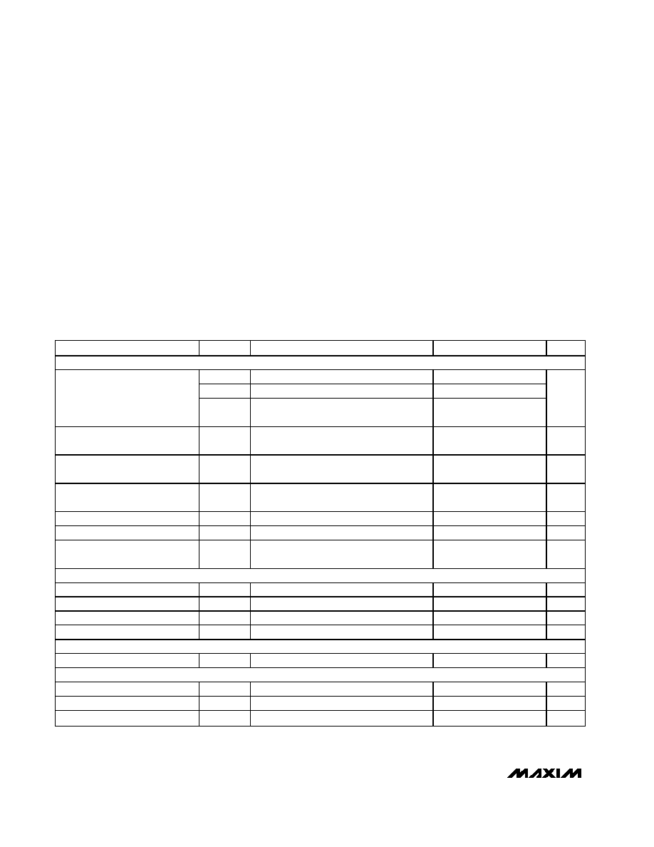
Ordering Information
19-2671; Rev 0; 10/02
For pricing, delivery, and ordering information, please contact Maxim/Dallas Direct! at
1-888-629-4642, or visit Maxim's website at www.maxim-ic.com.
PART
TEMP RANGE
PIN-PACKAGE
MAX3030ECSE
0∞C to +70∞C
16 SO (Narrow)
MAX3030ECUE
0∞C to +70∞C
16 TSSOP
MAX3030EESE
-40∞C to +85∞C
16 SO (Narrow)
MAX3030EEUE
-40∞C to +85∞C
16 TSSOP
MAX3031ECSE
0∞C to +70∞C
16 SO (Narrow)
MAX3031ECUE
0∞C to +70∞C
16 TSSOP
MAX3031EESE
-40∞C to +85∞C
16 SO (Narrow)
MAX3031EEUE
-40∞C to +85∞C
16 TSSOP
MAX3032ECSE
0∞C to +70∞C
16 SO (Narrow)
MAX3032ECUE
0∞C to +70∞C
16 TSSOP
MAX3032EESE
-40∞C to +85∞C
16 SO (Narrow)
MAX3032EEUE
-40∞C to +85∞C
16 TSSOP
MAX3033ECSE
0∞C to +70∞C
16 SO (Narrow)
MAX3033ECUE
0∞C to +70∞C
16 TSSOP
MAX3033EESE
-40∞C to +85∞C
16 SO (Narrow)
MAX3033EEUE
-40∞C to +85∞C
16 TSSOP
16
15
14
13
12
11
10
9
1
2
3
4
5
6
7
8
DI1
V
CC
DI4
DO4+
DO4-
DO3-
DO3+
DI3
TOP VIEW
MAX3030E/
MAX3031E
TSSOP/SO
DO1+
DO1-
DO2+
EN
DO2-
DI2
GND
EN
16
15
14
13
12
11
10
9
1
2
3
4
5
6
7
8
DI1
V
CC
DI4
DO4+
DO4-
DO3-
DO3+
DI3
MAX3032E/
MAX3033E
TSSOP/SO
DO1+
DO1-
DO2+
EN1&2
DO2-
DI2
GND
EN3&4
Pin Configurations
MAX3030E≠MAX3033E
±15kV ESD-Protected, 3.3V Quad
RS-422 Transmitters
2
_______________________________________________________________________________________
ABSOLUTE MAXIMUM RATINGS
DC ELECTRICAL CHARACTERISTICS
(3V
V
CC
3.6V, T
A
= T
MIN
to T
MAX
, unless otherwise noted. Typical values are at V
CC
= +3.3V and T
A
= +25∞C.) (Note 1)
Stresses beyond those listed under "Absolute Maximum Ratings" may cause permanent damage to the device. These are stress ratings only, and functional
operation of the device at these or any other conditions beyond those indicated in the operational sections of the specifications is not implied. Exposure to
absolute maximum rating conditions for extended periods may affect device reliability.
(All Voltages Are Referenced to Device Ground, Unless
Otherwise Noted)
V
CC
........................................................................................+6V
EN1&2, EN3&4, EN, EN............................................-0.3V to +6V
DI_ ............................................................................-0.3V to +6V
DO_+, DO_- (normal condition) .................-0.3V to (V
CC
+ 0.3V)
DO_+, DO_- (power-off or three-state condition).....-0.3V to +6V
Driver Output Current per Pin.........................................±150mA
Continuous Power Dissipation (T
A
= +70∞C)
16-Pin SO (derate 8.70mW/∞C above +70∞C)..............696mW
16-Pin TSSOP (derate 9.40mW/∞C above +70∞C) .......755mW
Operating Temperature Ranges
MAX303_EC_ ......................................................0∞C to +70∞C
MAX303_EE_ ...................................................-40∞C to +85∞C
Junction Temperature ......................................................+150∞C
Storage Temperature Range .............................-65∞C to +160∞C
Lead Temperature (soldering, 10s) .................................+300∞C
PARAMETER
SYMBOL
CONDITIONS
MIN
TYP
MAX
UNITS
DRIVER OUTPUT: DO_+, DO_-
V
OD1
R
L
= 100
, Figure 1
2.0
V
OD2
R
L
=
, Figure 1
3.6
Differential Driver Output
V
OD3
R
L
= 3.9k
(for compliance with V.11),
Figure 1
3.6
V
Change in Differential Output
Voltage
V
OD
R
L
= 100
(Note 2)
-0.4
+0.4
V
Driver Common-Mode Output
Voltage
V
OC
R
L
= 100
, Figure 1
3
V
Change in Common-Mode
Voltage
V
OC
R
L
= 100
(Note 2)
-0.4
+0.4
V
Three-State Leakage Current
I
OZ
V
OUT
= V
CC
or GND, driver disabled
±10
µA
Output Leakage Current
I
OFF
V
CC
= 0V, V
OUT
= 3V or 6V
20
µA
Driver Output Short-Circuit
Current
I
SC
V
OUT
= 0V, V
IN
= V
CC
or GND
(Note 3)
-150
mA
INPUTS: EN,
EN, EN1&2, EN3&4
Input High Voltage
V
IH
2.0
V
Input Low Voltage
V
IL
0.4
V
Input Current
I
LEAK
±2
µA
Hot-Swap Driver Input Current
I
HOTSWAP
EN, EN, EN1&2, EN3&4 (Note 4)
±200
µA
SUPPLY CURRENT
Supply Current
I
CC
No load
100
µA
THERMAL PROTECTION
Thermal-Shutdown Threshold
T
SH
160
∞C
Thermal-Shutdown Hysteresis
10
∞C
ESD Protection DO_
Human Body Model
±15
kV
MAX3030E≠MAX3033E
±15kV ESD-Protected, 3.3V Quad
RS-422 Transmitters
_______________________________________________________________________________________
3
SWITCHING CHARACTERISTICS--MAX3030E, MAX3032E
(3V
V
CC
3.6V, T
A
= T
MIN
to T
MAX
, unless otherwise noted. Typical values are at V
CC
= +3.3V and T
A
= +25∞C.)
PARAMETER
SYMBOL
CONDITIONS
MIN
TYP
MAX
UNITS
Driver Propagation Delay
Low to High
t
DPLH
Driver Propagation Delay
High to Low
t
DPHL
R
L
= 100
, C
L
= 50pF, Figures 2, 3
8
16
ns
Differential Transition Time, Low
to High
t
R
Differential Transition Time, High
to Low
t
F
R
L
= 100
, C
L
= 50pF (10% to 90%),
Figures 2, 3
10
ns
Differential Skew (Same Channel)
|t
DPLH
- t
DPHL
|
t
SK1
Skew Driver to Driver
(Same Device)
t
SK2
R
L
= 100
, C
L
= 50pF, V
CC
= 3.3V
±2
ns
Skew Part to Part
t
SK3
R
L
= 100
, C
L
= 50pF, V
CC
= 3.3V,
T
MAX
= +5∞C
5
ns
Maximum Data Rate
20
Mbps
Driver Enable to Output High
t
DZH
S2 closed, R
L
= 500
, C
L
= 50pF,
Figures 4, 5
50
ns
Driver Enable to Output Low
t
DZL
S1 closed, R
L
= 500
, C
L
= 50pF,
Figures 4, 5
50
ns
Driver Disable Time from Low
t
DLZ
S1 closed, R
L
= 500
, C
L
= 50pF,
Figures 4, 5
50
ns
Driver Disable Time from High
t
DHZ
S2 closed, R
L
= 500
, C
L
= 50pF,
Figures 4, 5
50
ns
SWITCHING CHARACTERISTICS--MAX3031E, MAX3033E
(3V
V
CC
3.6V, T
A
= T
MIN
to T
MAX
, unless otherwise noted. Typical values are at V
CC
= +3.3V and T
A
= +25∞C.)
PARAMETER
SYMBOL
CONDITIONS
MIN
TYP
MAX
UNITS
Driver Propagation Delay
Low to High
t
DPLH
Driver Propagation Delay
High to Low
t
DPHL
R
L
= 100
, C
L
= 50pF, Figures 2, 3
40
70
ns
Differential Transition Time,
Low to High
t
R
Differential Transition Time,
High to Low
t
F
R
L
= 100
, C
L
= 50pF (10% to 90%),
Figures 2, 3
15
50
ns
Differential Skew (Same Channel)
|t
DPLH
- t
DPHL
|
t
SK1
Skew Driver to Driver
(Same Device)
t
SK2
R
L
= 100
, C
L
= 50pF, V
CC
= 3.3V
±10
ns
MAX3030E≠MAX3033E
±15kV ESD-Protected, 3.3V Quad
RS-422 Transmitters
4
_______________________________________________________________________________________
SWITCHING CHARACTERISTICS--MAX3031E, MAX3033E (continued)
(3V
V
CC
3.6V, T
A
= T
MIN
to T
MAX
, unless otherwise noted. Typical values are at V
CC
= +3.3V and T
A
= +25∞C.)
PARAMETER
SYMBOL
CONDITIONS
MIN
TYP
MAX
UNITS
Skew Part to Part
t
SK3
R
L
= 100
, C
L
= 50pF, V
CC
= 3.3V,
T
MAX
= +5∞C
18
ns
Maximum Data Rate
2
Mbps
Driver Enable to Output High
t
DZH
S2 closed, R
L
= 500
, C
L
= 50pF,
Figures 4, 5
100
ns
Driver Enable to Output Low
t
DZL
S1 closed, R
L
= 500
, C
L
= 50pF,
Figures 4, 5
100
ns
Driver Disable Time from Low
t
DLZ
S1 closed, R
L
= 500
, C
L
= 50pF,
Figures 4, 5
150
ns
Driver Disable Time from High
t
DHZ
S2 closed, R
L
= 500
, C
L
= 50pF,
Figures 4, 5
150
ns
Note 1: All currents into the device are positive; all currents out of the device are negative. All voltages are referenced to device
ground, unless otherwise noted.
Note 2:
V
OD
and
V
OC
are the changes in V
OD
and V
OC
, respectively, when DI changes state.
Note 3: Only one output shorted at a time.
Note 4: This input current is for the hot-swap enable (EN_, EN, EN) inputs and is present until the first transition only. After the first
transition, the input reverts to a standard high-impedance CMOS input with input current I
LEAK
.
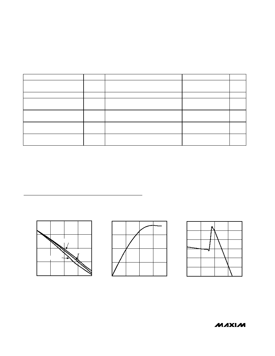
DIFFERENTIAL OUTPUT VOLTAGE
vs. OUTPUT CURRENT
MAX3030E toc01
OUTPUT CURRENT (mA)
DIFFERENTIAL OUTPUT VOLTAGE (V)
90
60
30
1
2
3
4
0
0
120
T
A
= 0
∞C
T
A
= +25
∞C
T
A
= +85
∞C
OUTPUT CURRENT
vs. TRANSMITTER OUTPUT LOW VOLTAGE
MAX3030E toc02
OUTPUT LOW VOLTAGE (V)
OUTPUT CURRENT (mA)
3
2
1
50
100
150
200
0
0
4
OUTPUT CURRENT
vs. TRANSMITTER OUTPUT HIGH VOLTAGE
MAX3030E toc03
OUTPUT HIGH VOLTAGE (V)
OUTPUT CURRENT (mA)
3
2
1
25
50
75
100
125
150
0
0
4
Typical Operating Characteristics
(V
CC
= +3.3V and T
A
= +25∞C, unless otherwise noted.)

MAX3030E≠MAX3033E
±15kV ESD-Protected, 3.3V Quad
RS-422 Transmitters
_______________________________________________________________________________________
5
SUPPLY CURRENT
vs. SUPPLY VOLTAGE
MAX3030E toc04
SUPPLY VOLTAGE (V)
SUPPLY CURRENT (
µ
A)
3
2
1
20
40
60
80
100
0
0
4
DRIVERS ENABLED
T
A
= +85
∞C
T
A
= +25
∞C
T
A
= 0
∞C
MAX3030E/MAX3032E
SUPPLY CURRENT vs. DATA RATE
MAX3030E toc05
DATA RATE (bps)
SUPPLY CURRENT (mA)
10M
1M
100k
10k
1k
5
10
15
20
25
30
0
0.1k
100M
NO RESISTIVE LOAD, C
L
= 200pF,
ALL FOUR
TRANSMITTERS
SWITCHING
MAX3031E/MAX3033E
SUPPLY CURRENT vs. DATA RATE
MAX3030E toc06
DATA RATE (bps)
SUPPLY CURRENT (mA)
1M
100k
10k
1k
0.5
1.0
1.5
2.0
2.5
0
0.1k
10M
NO RESISTIVE LOAD, C
L
= 200pF,
ALL FOUR
TRANSMITTERS
SWITCHING
MAX3030E/MAX3032E
SUPPLY CURRENT vs. DATA RATE
MAX3030E toc07
DATA RATE (bps)
SUPPLY CURRENT (mA)
10M
1M
100k
10k
1k
90
100
110
120
130
80
0.1k
100M
ALL FOUR TRANSMITTERS
LOADED AND SWITCHING
R
L
= 100
, C
L
= 200pF
MAX3031E/MAX3033E
SUPPLY CURRENT vs. DATA RATE
MAX3030E toc08
DATA RATE (bps)
SUPPLY CURRENT (mA)
1M
100k
10k
1k
91
94
97
100
88
0.1k
10M
ALL FOUR TRANSMITTERS
LOADED AND SWITCHING
R
L
= 100
, C
L
= 200pF
MAX3030E
DRIVER PROPAGATION DELAY
(LOW TO HIGH)
MAX3030E toc09
10ns/div
DIFFERENTIAL
OUTPUT
2V/div
DI_
1V/div
MAX3030E
DRIVER PROPAGATION DELAY
(HIGH TO LOW)
MAX3030E toc10
10ns/div
DIFFERENTIAL
OUTPUT
2V/div
DI_
1V/div
MAX3031E
DRIVER PROPAGATION DELAY
(LOW TO HIGH)
MAX3030E toc11
20ns/div
DIFFERENTIAL
OUTPUT
2V/div
DI_
1V/div
MAX3031E
DRIVER PROPAGATION DELAY
(HIGH TO LOW)
MAX3030E toc12
20ns/div
DIFFERENTIAL
OUTPUT
2V/div
DI_
1V/div
Typical Operating Characteristics (continued)
(V
CC
= +3.3V and T
A
= +25∞C, unless otherwise noted.)