 | –≠–ª–µ–∫—Ç—Ä–æ–Ω–Ω—ã–π –∫–æ–º–ø–æ–Ω–µ–Ω—Ç: MAX3062E | –°–∫–∞—á–∞—Ç—å:  PDF PDF  ZIP ZIP |

MAX3060E/MAX3061E/MAX3062E
±15kV ESD-Protected, Fail-Safe, 20Mbps, Slew-Rate-
Limited RS-485/RS-422 Transceivers in a SOT
________________________________________________________________ Maxim Integrated Products
1
For pricing, delivery, and ordering information, please contact Maxim/Dallas Direct! at
1-888-629-4642, or visit Maxim's website at www.maxim-ic.com.
General Description
The MAX3060E/MAX3061E/MAX3062E high-speed
transceivers for RS-485/RS-422 communication contain
one driver and one receiver. These devices feature fail-
safe circuitry, which guarantees a logic-high receiver
output when the receiver inputs are open or shorted.
This means that the receiver output is a logic high if all
transmitters on a terminated bus are disabled (high
impedance). These devices also feature hot-swap cir-
cuitry that eliminates data glitches during hot insertion.
The MAX3060E features slew-rate-limited drivers that
minimize EMI and reduce reflections caused by
improperly terminated cables, allowing error-free data
transmission up to 115kbps. The MAX3061E, also slew-
rate limited, transmits up to 500kbps. The MAX3062E
driver is not slew-rate limited, allowing transmit speeds
up to 20Mbps. All transmitter outputs are protected to
±15kV using the Human Body Model.
These transceivers typically draw 910µA of supply
current when unloaded, or 790µA when fully loaded
with the drivers disabled.
All devices have a 1/8-unit-load receiver input imped-
ance that allows up to 256 transceivers on the bus. These
devices are intended for half-duplex communication.
Applications
RS-422/RS-485 Communications
Level Translators
Transceivers for EMI-Sensitive Applications
Industrial-Control Local-Area Networks
Features
o True Fail-Safe Receiver While Maintaining
EIA/TIA-485 Compatibility
o Enhanced Slew-Rate Limiting Facilitates
Error-Free Data Transmission (MAX3060E and
MAX3061E)
o 1nA Low-Current Shutdown Mode
o Hot-Swappable for Telecom Applications
o ESD Protection: ±15kV Human Body Model
o Allow Up to 256 Transceivers on the Bus
o Space-Saving 8-Pin SOT23 Package
19-2536; Rev 0; 7/02
Ordering Information
PART
TEMP RANGE
PIN-
PACKAGE
TOP
MARK
MAX3060EEKA-T
-40∞C to +85∞C
8 SOT23-8
AAKI
MAX3061EEKA-T
-40∞C to +85∞C
8 SOT23-8
AAKJ
MAX3062EEKA-T
-40∞C to +85∞C
8 SOT23-8
AAKK
Selector Guide
PART
DATA
RATE
(Mbps)
SLEW-
RATE
LIMITED
TRANSCEIVERS
ON BUS
MAX3060E
0.115
Yes
256
MAX3061E
0.5
Yes
256
MAX3062E
20
No
256
MAX3060E
MAX3061E
MAX3062E
1
2
3
4
8
5
V
CC
0.1
µF
GND
DI
DE
RE
RO
R
D
Rt
Rt
7
6
D
R
DE
RE
DI
RO
A
B
B
A
TOP VIEW
+5V
Typical Operating Circuit/Pin Configuration

MAX3060E/MAX3061E/MAX3062E
±15kV ESD-Protected, Fail-Safe, 20Mbps, Slew-Rate-
Limited RS-485/RS-422 Transceivers in a SOT
2
_______________________________________________________________________________________
ABSOLUTE MAXIMUM RATINGS
DC ELECTRICAL CHARACTERISTICS
(V
CC
= +5V ±5%, T
A
= T
MIN
to T
MAX
, unless otherwise noted. Typical values are at V
CC
= +5V and T
A
= +25∞C.) (Notes 1, 2)
Stresses beyond those listed under "Absolute Maximum Ratings" may cause permanent damage to the device. These are stress ratings only, and functional
operation of the device at these or any other conditions beyond those indicated in the operational sections of the specifications is not implied. Exposure to
absolute maximum rating conditions for extended periods may affect device reliability.
All Voltages with Respect to GND
Supply Voltage (V
CC
) ............................................................+7V
Input Voltage (RE, DE, DI)..........................-0.3V to (V
CC
+ 0.3V)
Driver Output/Receiver Input Voltage (A, B) .......-7.5V to +12.5V
Receiver Output Voltage (RO)....................-0.3V to (V
CC
+ 0.3V)
Continuous Power Dissipation (T
A
= +70∞C)
8-Pin SOT23 (derate 8.9mW/∞C above +70∞C)............714mW
Operating Temperature Range
MAX306_EE_ _ ................................................-40∞C to +85∞C
Storage Temperature Range .............................-65∞C to +150∞C
Junction Temperature ......................................................+150∞C
Lead Temperature (soldering, 10s) .................................+300∞C
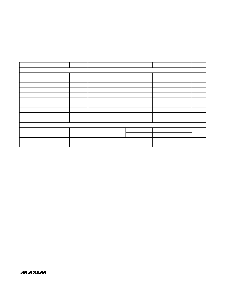
PARAMETER
SYMBOL
CONDITIONS
MIN
TYP
MAX
UNITS
DRIVER
Differential Driver Output
(No Load)
V
OD1
V
CC
= 5V
5
V
Figure 1, R = 50
(RS-422)
2.0
Differential Driver Output
V
OD2
Figure 1, R = 27
(RS-485)
1.5
V
Change in Magnitude of
Differential Output Voltage
V
OD
Figure 1, R = 50
or R = 27 (Note 3)
0.2
V
Driver Common-Mode Output
Voltage
V
OC
Figure 1, R = 50
or R = 27
3
V
Change in Magnitude of
Common-Mode Voltage
V
OC
Figure 1, R = 50
or R = 27 (Note 3)
0.2
V
Input High Voltage
V
IH
DE, DI, RE
2.0
V
Input Low Voltage
V
IL
DE, DI, RE
0.8
V
DI Input Hysteresis
V
HYS
100
mV
Input Current
I
IN1
DE, DI, RE
±1
µA
Hot-Swap Driver Input Current
I
HOTSWAP
DE, RE (Note 4)
±200
µA
V
IN
= +12V
125
Input Current (A and B)
I
IN2
DE = GND,
V
CC
= GND or 5.25V
V
IN
= -7V
-100
µA
Driver Short-Circuit Output
Current
V
OD1
-7V
V
OUT
+12V, T
A
= +25∞C (Note 5)
±15
±250
mA
IEC 1000-4-2 Air-Gap Discharge
±7
IEC 1000-4-2 Contact Discharge
±7
ESD Protection for A, B
Human Body Model
±15
kV
MAX3060E/MAX3061E/MAX3062E
±15kV ESD-Protected, Fail-Safe, 20Mbps, Slew-Rate-
Limited RS-485/RS-422 Transceivers in a SOT
_______________________________________________________________________________________
3
DC ELECTRICAL CHARACTERISTICS (continued)
(V
CC
= +5V ±5%, T
A
= T
MIN
to T
MAX
, unless otherwise noted. Typical values are at V
CC
= +5V and T
A
= +25∞C.) (Notes 1, 2)
PARAMETER
SYMBOL
CONDITIONS
MIN
TYP
MAX
UNITS
RECEIVER
Receiver Differential Threshold
Voltage
V
TH
-7V
VCM +12V
-200
-125
-50
mV
Receiver Input Hysteresis
V
TH
25
mV
Receiver Output High Voltage
V
OH
I
O
= -4mA, V
ID
= -50mV
V
CC
- 1.5
V
Receiver Output Low Voltage
V
OL
I
O
= 4mA, V
ID
= -200mV
0.4
V
Three-State Output Current at
Receiver
I
OZR
0V
V
O
V
CC
0.01
±1
µA
Receiver Input Resistance
R
IN
-7V
V
CM
+12V
96
k
Receiver Output Short-Circuit
Current
I
OSR
0V
V
RO
V
CC
±8
±80
mA
SUPPLY CURRENT
DE = RE = GND
790
1400
Supply Current
I
CC
No load,
DI = GND or V
CC
DE = RE = V
CC
910
1500
µA
Supply Current in Shutdown
Mode
I
SHDN
DE = GND, RE = V
CC
0.001
1
µA

MAX3060E/MAX3061E/MAX3062E
±15kV ESD-Protected, Fail-Safe, 20Mbps, Slew-Rate-
Limited RS-485/RS-422 Transceivers in a SOT
4
_______________________________________________________________________________________
SWITCHING CHARACTERISTICS--MAX3060E
(V
CC
= +5V ±5%, T
A
= T
MIN
to T
MAX
, unless otherwise noted. Typical values are at V
CC
= +5V and T
A
= +25∞C.) (Notes 1, 2)
PARAMETER
SYMBOL
CONDITIONS
MIN
TYP
MAX
UNITS
Driver Input to Output
t
DPLH
, t
DPHL
Figures 3 and 5, R
DIFF
= 54
,
C
DIFF
= 50pF
1.0
1.7
2.4
µs
Driver Output Skew
(t
DPLH
- t
DPHL
)
t
DSKEW
Figures 3 and 5, R
DIFF
= 54
,
C
DIFF
= 50pF
-200
-7
+200
ns
Driver Rise or Fall Time
t
DR
, t
DF
Figures 3 and 5, R
DIFF
= 54
,
C
DIFF
= 50pF
1.3
1.85
2.5
µs
Maximum Data Rate
f
MAX
115
kbps
Driver Enable to Output High
t
DZH
Figures 4 and 6, C
L
= 100pF, S2 closed
0.6
1.5
µs
Driver Enable to Output Low
t
DZL
Figures 4 and 6, C
L
= 100pF, S1 closed
0.5
1.5
µs
Driver Disable Time from Low
t
DLZ
Figures 4 and 6, C
L
= 15pF, S1 closed
60
200
ns
Driver Disable Time from High
t
DHZ
Figures 4 and 6, C
L
= 15pF, S2 closed
85
200
ns
Receiver Input to Output
t
RPLH
,
t
RPHL
Figures 7 and 9; | V
ID
|
2.0V;
rise and fall time of V
ID
4ns, C
L
= 15pF
47
80
ns
Differential Receiver Skew
(t
RPLH
- t
RPHL
)
t
RSKD
Figures 7 and 9; | V
ID
|
2.0V;
rise and fall time of V
ID
4ns, C
L
= 15pF
-10
-3
+10
ns
Receiver Enable to Output Low
t
RZL
Figures 2 and 8, C
L
= 15pF, S1 closed
50
ns
Receiver Enable to Output High
t
RZH
Figures 2 and 8, C
L
= 15pF, S2 closed
50
ns
Receiver Disable Time from Low
t
RLZ
Figures 2 and 8, C
L
= 15pF, S1 closed
50
ns
Receiver Disable Time from High
t
RHZ
Figures 2 and 8, C
L
= 15pF, S2 closed
50
ns
Time to Shutdown
t
SHDN
(Note 6)
50
180
600
ns
Driver Enable from Shutdown to
Output High
t
DZH(SHDN)
Figures 4 and 6, C
L
= 100pF, S2 closed
2
µs
Driver Enable from Shutdown to
Output Low
t
DZL(SHDN)
Figures 4 and 6, C
L
= 100pF, S1 closed
2
µs
Receiver Enable from Shutdown
to Output High
t
RZH(SHDN)
Figures 2 and 8, C
L
= 15pF, S2 closed
1.5
µs
Receiver Enable from Shutdown
to Output Low
t
RZL(SHDN)
Figures 2 and 8, C
L
= 15pF, S1 closed
1.5
µs

MAX3060E/MAX3061E/MAX3062E
±15kV ESD-Protected, Fail-Safe, 20Mbps, Slew-Rate-
Limited RS-485/RS-422 Transceivers in a SOT
_______________________________________________________________________________________
5
SWITCHING CHARACTERISTICS--MAX3061E
(V
CC
= +5V ±5%, T
A
= T
MIN
to T
MAX
, unless otherwise noted. Typical values are at V
CC
= +5V and T
A
= +25∞C.) (Notes 1, 2)
PARAMETER
SYMBOL
CONDITIONS
MIN
TYP
MAX
UNITS
Driver Input to Output
t
DPLH
,
t
DPHL
Figures 3 and 5, R
DIFF
= 54
,
C
DIFF
= 50pF
250
470
800
ns
Driver Output Skew
(t
DPLH
- t
DPHL
)
t
DSKEW
Figures 3 and 5, R
DIFF
= 54
,
C
DIFF
= 50pF
-100
-4
+100
ns
Driver Rise or Fall Time
t
DR
, t
DF
Figures 3 and 5, R
DIFF
= 54
,
C
DIFF
= 50pF
200
530
750
ns
Maximum Data Rate
f
MAX
500
kbps
Driver Enable to Output High
t
DZH
Figures 4 and 6, C
L
= 100pF, S2 closed
330
1000
ns
Driver Enable to Output Low
t
DZL
Figures 4 and 6, C
L
= 100pF, S1 closed
200
1000
ns
Driver Disable Time from Low
t
DLZ
Figures 4 and 6, C
L
= 15pF, S1 closed
60
200
ns
Driver Disable Time from High
t
DHZ
Figures 4 and 6, C
L
= 15pF, S2 closed
80
200
ns
Receiver Input to Output
t
RPLH
,
t
RPHL
Figures 7 and 9; | V
ID
|
2.0V;
rise and fall time of V
ID
4ns, C
L
= 15pF
47
80
ns
Differential Receiver Skew
(t
RPLH
- t
RPHL
)
t
RSKD
Figures 7 and 9; | V
ID
|
2.0V;
rise and fall time of V
ID
4ns, C
L
= 15pF
-10
-3
+10
ns
Receiver Enable to Output Low
t
RZL
Figures 2 and 8, C
L
= 15pF, S1 closed
50
ns
Receiver Enable to Output High
t
RZH
Figures 2 and 8, C
L
= 15pF, S2 closed
50
ns
Receiver Disable Time from Low
t
RLZ
Figures 2 and 8, C
L
= 15pF, S1 closed
50
ns
Receiver Disable Time from High
t
RHZ
Figures 2 and 8, C
L
= 15pF, S2 closed
50
ns
Time to Shutdown
t
SHDN
(Note 6)
50
180
600
ns
Driver Enable from Shutdown to
Output High
t
DZH(SHDN
Figures 4 and 6, C
L
= 100pF, S2 closed
1.5
µs
Driver Enable from Shutdown to
Output Low
t
DZL(SHDN)
Figures 4 and 6, C
L
= 100pF, S1 closed
1.5
µs
Receiver Enable from Shutdown
to Output High
t
RZH(SHDN)
Figures 2 and 8, C
L
= 15pF, S2 closed
1.5
µs
Receiver Enable from Shutdown
to Output Low
t
RZL(SHDN)
Figures 2 and 8, C
L
= 15pF, S1 closed
1.5
µs