 | ÐлекÑÑоннÑй компоненÑ: MAX3182 | СкаÑаÑÑ:  PDF PDF  ZIP ZIP |
Äîêóìåíòàöèÿ è îïèñàíèÿ www.docs.chipfind.ru
For free samples & the latest literature: http://www.maxim-ic.com, or phone 1-800-998-8800.
For small orders, phone 1-800-835-8769.
General Description
The MAX3180MAX3183 are single RS-232 receivers in
a SOT23-5 package for space- and cost-constrained
applications requiring minimal RS-232 communications.
These devices minimize power and heat dissipation by
consuming only 0.5µA supply current from a +3.0V to
+5.5V supply voltage. They guarantee true RS-232 per-
formance up to a 1.5Mbps data rate.
The MAX3180/MAX3182 feature a three-state TTL/
CMOS receiver output that is controlled by an EN logic
input. The MAX3181/MAX3183 feature an INVALID out-
put that indicates valid RS-232 signals at the receiver
input for applications requiring automatic system wake-
up. The MAX3180/MAX3181 receivers have a standard
inverting output, while the MAX3182/MAX3183 receivers
have a noninverting output.
Applications
Diagnostic Ports
Set-Top Boxes
Telecommunications
Digital Cameras
Networking Equipment
Hand-Held Equipment
Features
o
Tiny SOT23-5 Package
o
0.5µA Supply Current
o
1.5Mbps Guaranteed Data Rate
o
Meet EIA/TIA-232 and V.28/V.24 Specifications
Down to V
CC
= +3.0V
o
INVALID
Output Indicates Valid RS-232 Signal at
Receiver Input (MAX3181/MAX3183)
o
Three-State TTL/CMOS Receiver Output
(MAX3180/MAX3182)
o
Noninverting RS-232 Output (MAX3182/MAX3183)
MAX3180MAX3183
+3V to +5.5V, 1.5Mbps
RS-232 Receivers in SOT23-5
________________________________________________________________
Maxim Integrated Products
1
19-1444; Rev 1; 7/99
Ordering Information
PART
MAX3180
EUK-T
TOP
MARK
-40°C to +85°C
TEMP. RANGE
PIN-
PACKAGE
5 SOT23-5
ADKF
MAX3181
EUK-T -40°C to +85°C
5 SOT23-5
ADKG
MAX3182
EUK-T -40°C to +85°C
5 SOT23-5
ADKH
MAX3183
EUK-T -40°C to +85°C
5 SOT23-5
ADKI
Selector Guide
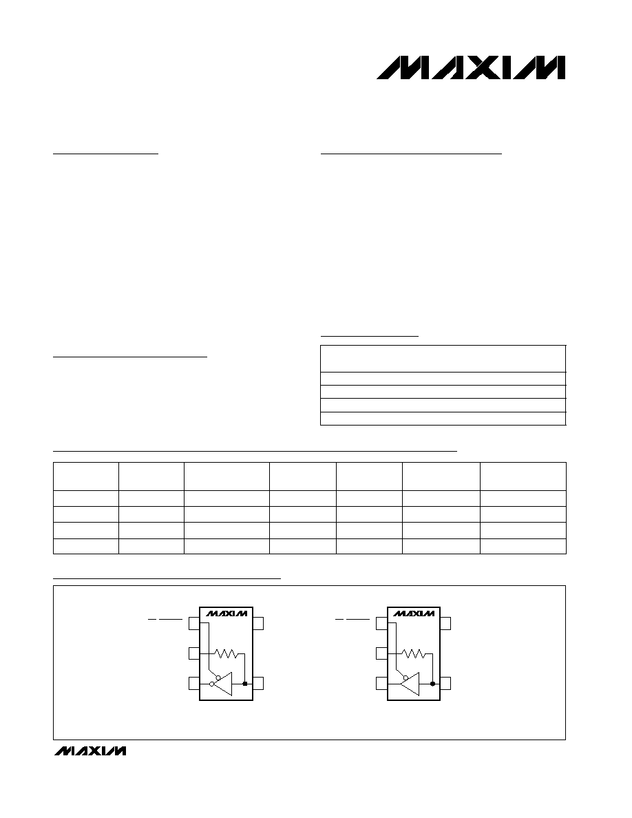
Pin Configurations/Functional Diagrams
MAX3180
SUPPLY
CURRENT (µA)
0.5
INVALID
OUTPUT
--
INVERTING
ROUT
NONINVERTING
ROUT
--
MAX3181
0.5
--
MAX3182
0.5
--
--
MAX3183
0.5
--
GND
RIN
ROUT
1
5
5k
V
CC
EN (INVALID)
MAX3180
MAX3181
SOT23-5
TOP VIEW
2
3
4
GND
RIN
ROUT
1
5
5k
V
CC
EN (INVALID)
MAX3182
MAX3183
SOT23-5
2
3
4
( ) ARE FOR MAX3181/MAX3183 ONLY
.
EN
INPUT
--
--
PART
SOT23-5
PACKAGE
SOT23-5
SOT23-5
SOT23-5
MAX3180MAX3183
+3V to +5.5V, 1.5Mbps
RS-232 Receivers in SOT23-5
2
_______________________________________________________________________________________
ABSOLUTE MAXIMUM RATINGS
ELECTRICAL CHARACTERISTICS
(V
CC
= +3.0V to +5.5V, T
A
= T
MIN
to T
MAX
, unless otherwise noted. Typical values are at V
CC
= +5.0V and T
A
= +25°C.) (Note 1)
Stresses beyond those listed under "Absolute Maximum Ratings" may cause permanent damage to the device. These are stress ratings only, and functional
operation of the device at these or any other conditions beyond those indicated in the operational sections of the specifications is not implied. Exposure to
absolute maximum rating conditions for extended periods may affect device reliability.
V
CC
to GND ..............................................................-0.3V to +6V
RIN to GND ..........................................................................±25V
EN, ROUT, INVALID to GND ......................-0.3V to (V
CC
+ 0.3V)
Continuous Power Dissipation (T
A
= +70°C)
SOT23-5 (derate 7.1mW/°C above +70°C)...................571mW
Operating Temperature Range ...........................-40°C to +85°C
Storage Temperature Range .............................-65°C to +150°C
Lead Temperature (soldering, 10sec) .............................+300°C
I
SOURCE
= 1.0mA
V
CC
= 3.3V or 5V, RIN = V
CC
or GND, no load
Negative threshold
Positive threshold
V
CC
= 5.0V
V
CC
= 3.3V
I
SINK
= 1.6mA
V
CC
= 5.0V
V
CC
= 3.3V
V
CC
= 3.3V
V
CC
= 5.0V
CONDITIONS
k
3
5
7
R
RIN
Input Resistance
V
V
CC
- V
CC
-
0.6
0.1
V
OH
Output Voltage High
V
-0.3
0.3
V
ITOL
RIN Threshold to INVALID
Output Low
V
-2.7
V
ITOH
I
SOURCE
= 1.0mA
2.7
V
RIN Threshold to INVALID
Output High
mV
300
V
HYST
Input Hysteresis
V
1.8
2.7
V
ITH
Input Threshold High
1.5
2.4
V
CC
-
0.6
V
IOH
V
0.8
1.5
V
ITL
Input Threshold Low
0.6
1.2
INVALID Output Voltage High
V
-25
25
V
RIN
Input Voltage Range
µA
0.5
5
I
CC
Supply Current
V
3.0
5.5
V
CC
Supply Voltage
V
0.4
V
IOL
INVALID Output Voltage Low
µA
±0.01
±1.0
I
EN
Leakage Current
V
0.8
V
IL
Logic Threshold Low
2.0
I
SINK
= 1.6mA
V
2.4
V
IH
Logic Threshold High
UNITS
MIN
TYP
MAX
SYMBOL
PARAMETER
Receiver disabled
V
0.4
V
OL
Output Voltage Low
µA
±0.05
±10
I
ROUT
Output Leakage Current
DC CHARACTERISTICS
LOGIC INPUT (
EN
)
LOGIC OUTPUT
RECEIVER INPUT
RECEIVER OUTPUT
MAX3180MAX3183
+3V to +5.5V, 1.5Mbps
RS-232 Receivers in SOT23-5
_______________________________________________________________________________________
3
ELECTRICAL CHARACTERISTICS (continued)
(V
CC
= +3.0V to +5.5V, T
A
= T
MIN
to T
MAX
, unless otherwise noted. Typical values are at V
CC
= +5.0V and T
A
= +25°C.) (Note 1)
ns
250
t
INVH
Receiver Positive or Negative
Threshold to INVALID High
ns
200
t
ROD
Receiver Output Disable Time
µs
30
t
INVL
Receiver Positive or Negative
Threshold to INVALID Low
RIN to ROUT; C
L
= 150pF
µs
0.15
CONDITIONS
t
PHL
Receiver Propagation Delay,
High-to-Low
RIN to ROUT; C
L
= 150pF
µs
0.15
t
PLH
Receiver Propagation Delay,
Low-to-High
|
t
PHL
- t
PLH
|
, Figure 1
UNITS
MIN
TYP
MAX
SYMBOL
PARAMETER
C
L
= 50pF
ns
200
t
ROE
Receiver Output Enable Time
ns
50
t
RS
Receiver Skew
Mbps
1.5
Maximum Data Rate
TIMING CHARACTERISTICS
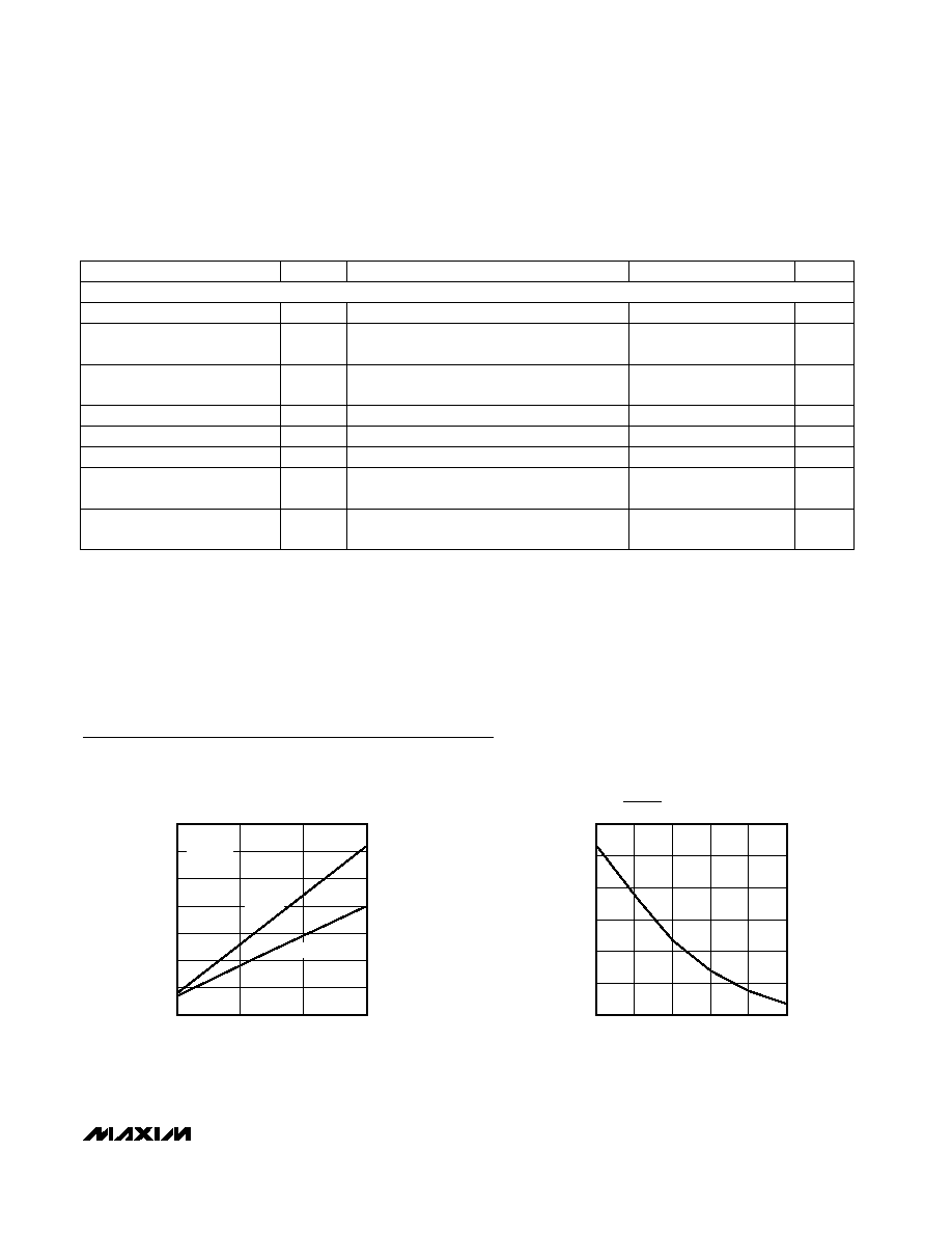
Typical Operating Characteristics
(V
CC
= +5V, T
A
= +25°C, unless otherwise noted.)
0
0.2
0.1
0.4
0.3
0.6
0.5
0.7
0
0.5
1.0
1.5
SUPPLY CURRENT vs. DATA RATE
MAX3180-01
DATA RATE (Mbps)
SUPPLY CURRENT (mA)
R
L
= 50k
C
L
= 100pF
V
CC
= 5V
V
CC
= 3.3V
230
270
250
290
330
310
350
3.0
3.5
5.0
4.5
4.0
5.5
RIN TO INVALID HIGH vs. SUPPLY VOLTAGE
MAX3180-02
V
CC
(V)
t
INVH
(ns)
Note 1:
Specifications are 100% tested at T
A
= +25°C. Limits over temperature are guaranteed by design.
MAX3180MAX3183
+3V to +5.5V, 1.5Mbps
RS-232 Receivers in SOT23-5
4
_______________________________________________________________________________________
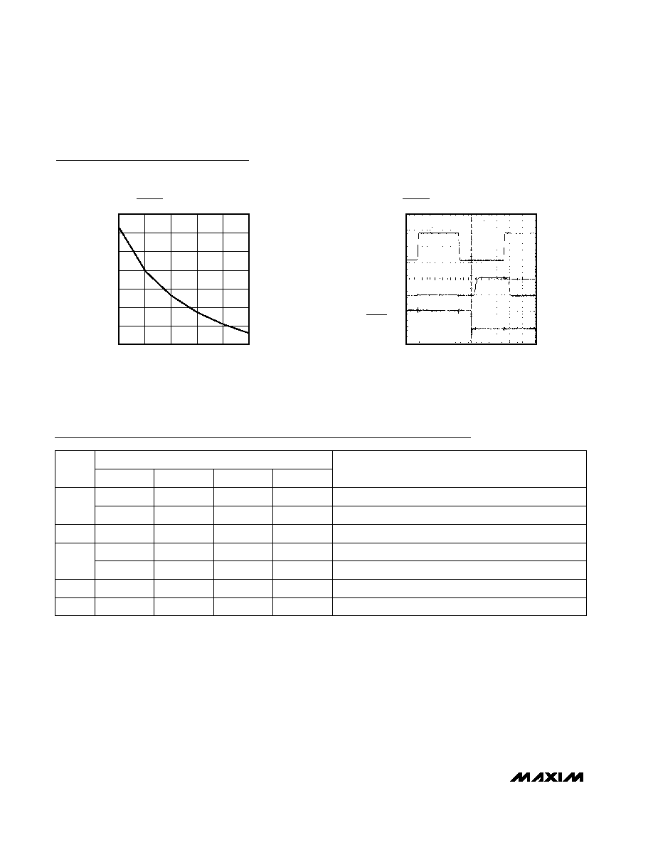
25
35
30
45
40
55
50
60
3.0
3.5
4.0
4.5
5.0
5.5
RIN TO INVALID LOW vs. SUPPLY VOLTAGE
MAX3180-03
V
CC
(V)
t
INVL
(
µ
s)
Typical Operating Characteristics (continued)
(V
CC
= +5V, T
A
= +25°C, unless otherwise noted.)
5V
0
10V
0
-10V
RIN
ROUT
ENABLE
5V
0
500ns/div
MAX3180
ENABLE ASSERTION TO ROUT RESPONSE
MAX3180-04
V
CC
= 5.0V
R
L
= 50k
C
L
= 100pF
20V
Pin Description
MAX3181
1
EN
Receiver Output Enable
NAME
EN
MAX3180
Noninverting Receiver Output
FUNCTION
MAX3182
PIN
ROUT
Output of the Valid Input Detector
2
GND
Ground
GND
3
ROUT
Inverting Receiver Output
4
RIN
Receiver Input
RIN
5
V
CC
Supply Voltage
V
CC
MAX3183
INVALID
GND
ROUT
RIN
V
CC
INVALID
GND
ROUT
RIN
V
CC
Detailed Description
The MAX3180MAX3183 are EIA/TIA-232 and V.28/
V.24 communications receivers that convert RS-232
signals to CMOS logic levels. The devices operate on a
supply voltage of +3V to +5.5V and have a 1.5Mbps
data rate capability. They achieve a 0.5µA typical sup-
ply current. The MAX3180/MAX3182 have a receiver
enable control (EN), while the MAX3181/MAX3183 con-
tain a signal invalid output (INVALID). The MAX3180/
MAX3181 invert the ROUT signal relative to RIN. The
MAX3182/MAX3183 are not inverted. The devices
come in SOT23-5 packages.
Signal Invalid Detector
If no valid signal levels appear on RIN for 30µs (typ),
INVALID goes low. This event typically occurs if the RS-
232 cable is disconnected or if the connected peripher-
al transmitter is turned off. INVALID goes high when a
valid level is applied to the RS-232 receiver input.
Figure 2 shows the input levels and timing diagram for
INVALID operation.
Enable Input
The MAX3180/MAX3182 feature an enable input. Drive
EN high to force ROUT into a high-impedance state. In
this state, the devices ignore incoming RS-232 signals.
Drive EN low for normal operation.
Power-Supply Decoupling
In most circumstances, a 0.1µF V
CC
bypass capacitor
is adequate for power-supply decoupling. Connect the
bypass capacitor as close to the IC as possible.
MAX3180MAX3183
+3V to +5.5V, 1.5Mbps
RS-232 Receivers in SOT23-5
_______________________________________________________________________________________
5
50%
50%
50%
0
RIN
5V
ROUT
50%
t
PLH
t
PHL
V
OL
V
OH
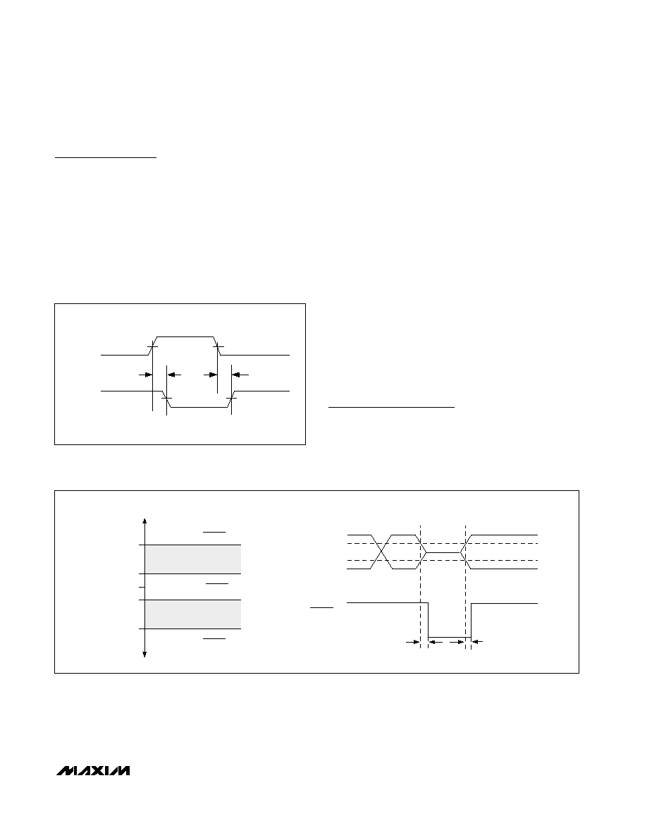
Figure 1. Receiver Propagation-Delay Timing
VALID SIGNALS (INVALID = 1)
INVALID SIGNALS (INVALID = 0)
VALID SIGNALS (INVALID = 1)
RECEIVER INPUT LEVELS
-2.7V
-0.3V
+2.7V
+0.3V
0
INDETERMINATE
INDETERMINATE
0
V
CC
t
INVL
INVALID
REGION
RECEIVER
INPUT
VOLTAGE
(V)
INVALID
OUTPUT
(V)
t
INVH
Figure 2. Input Levels and INVALID Timing
Chip Information
TRANSISTOR COUNT: 41