 | ÐлекÑÑоннÑй компоненÑ: MAX3230E | СкаÑаÑÑ:  PDF PDF  ZIP ZIP |
Äîêóìåíòàöèÿ è îïèñàíèÿ www.docs.chipfind.ru
General Description
The MAX3230E/MAX3231E are +2.5V to +5.5V pow-
ered EIA/TIA-232 and V.28/V.24 communications inter-
faces with low power requirements, high data-rate
capabilities, and enhanced electrostatic discharge
(ESD) protection, in a chip-scale package (UCSPTM).
All transmitter outputs and receiver inputs are protect-
ed to ±15kV using IEC 1000-4-2 Air-Gap Discharge,
±8kV using IEC 1000-4-2 Contact Discharge, and
±15kV using the Human Body Model.
The MAX3230E/MAX3231E achieve a 1µA supply cur-
rent with Maxim's AutoShutdownTM feature. They save
power without changing the existing BIOS or operating
systems by entering low-power shutdown mode when
the RS-232 cable is disconnected, or when the trans-
mitters of the connected peripherals are off.
The transceivers have a proprietary low-dropout trans-
mitter output stage, delivering RS-232-compliant perfor-
mance from a +3.1V to +5.5V supply, and RS-232-
compatible performance with a supply voltage as low
as +2.5V. The dual charge pump requires only four,
small 0.1µF capacitors for operation from a +3.0V sup-
ply. Each device is guaranteed to run at data rates of
250kbps while maintaining RS-232 output levels.
The MAX3230E/MAX3231E offer a separate power-sup-
ply input for the logic interface, allowing configurable
logic levels on the receiver outputs and transmitter
inputs. Operating over a +1.65V to V
CC
range, V
L
pro-
vides the MAX3230E/MAX3231E compatibility with mul-
tiple logic families.
The MAX3231E contains one receiver and one transmit-
ter. The MAX3230E contains two receivers and two trans-
mitters. The MAX3230E/MAX3231E are available in tiny
chip-scale packaging and are specified across the
extended industrial (-40°C to +85°C) temperature range.
Applications
Personal Digital Assistants
Cell-Phone Data Lump Cables
Set-Top Boxes
Hand-Held Devices
Cell Phones
Features
6 x 5 Chip-Scale Packaging (UCSP)
ESD Protection for RS-232 I/O Pins
±15kV--IEC 1000-4-2 Air-Gap Discharge
±8kV--IEC 1000-4-2 Contact Discharge
±15kV--Human Body Model
1µA Low-Power AutoShutdown
250kbps Guaranteed Data Rate
Meet EIA/TIA-232 Specifications Down to +3.1V
RS-232 Compatible to +2.5V Allows Operation
from Single Li+ Cell
Small 0.1µF Capacitors
Configurable Logic Levels
MAX3230E/MAX3231E
±15kV ESD-Protected +2.5V to +5.5V
RS-232 Transceivers in UCSP
________________________________________________________________ Maxim Integrated Products
1
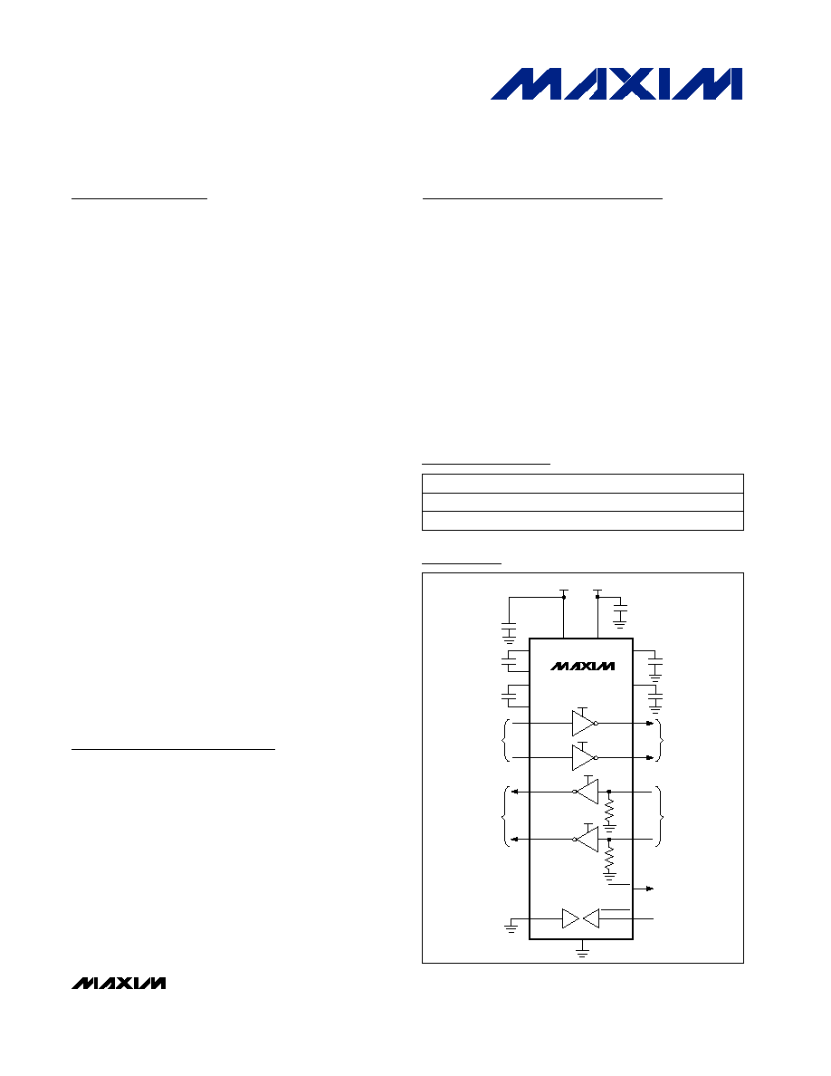
MAX3230E
5k
T2OUT
T2IN
TTL/CMOS
INPUTS
C2-
C2+
C1-
C1+
A1
A5
C1
D1
A2
A3
A6
B6
B1
A4
E3
E4
E2
E1
C5
B5
V-
V+
V
CC
2.5V TO 5.5V
C4
0.1µF
C3
0.1µF
C1
0.1µF
C
BYPASS
C2
0.1µF
0.1µF
FORCEOFF
FORCEON
INVALID
T1OUT
T1IN
GND
V
L
TO POWER-
MANAGEMENT
UNIT
RS-232
OUTPUTS
V
L
V
L
V
L
1.65V TO 5.5V
5k
R2IN
R2OUT
TTL/CMOS
OUTPUTS
D6
C6
E6
E5
R1IN
R1OUT
RS-232
INPUTS
V
L
V
L
0.1µF
Typical Operating Circuits
19-3250; Rev 0; 5/04
For pricing, delivery, and ordering information, please contact Maxim/Dallas Direct! at
1-888-629-4642, or visit Maxim's website at www.maxim-ic.com.
Ordering Information
PART
TEMP RANGE
BUMP-PACKAGE
M A X3 2 3 0 E
E BV - T
-40°C to +85°C
6 x 5 UCSP
M A X3 2 3 1 E
E BV - T
-40°C to +85°C
6 x 5 UCSP
UCSP is a trademark of Maxim Integrated Products, Inc.
AutoShutdown is a trademark of Maxim Integrated Products, Inc.
Typical Operating Circuits continued at end of data sheet.
Pin Configurations appear at end of data sheet.
MAX3230E/MAX3231E
±15kV ESD-Protected +2.5V to +5.5V
RS-232 Transceivers in UCSP
2
_______________________________________________________________________________________
ABSOLUTE MAXIMUM RATINGS
Stresses beyond those listed under "Absolute Maximum Ratings" may cause permanent damage to the device. These are stress ratings only, and functional
operation of the device at these or any other conditions beyond those indicated in the operational sections of the specifications is not implied. Exposure to
absolute maximum rating conditions for extended periods may affect device reliability.
V
CC
to GND ...........................................................-0.3V to +6.0V
V+ to GND .............................................................-0.3V to +7.0V
V- to GND ..............................................................+0.3V to -7.0V
V+ to |V-| (Note 1) ................................................................+13V
V
L
to GND..............................................................-0.3V to +6.0V
Input Voltages
T_IN_, FORCEON, FORCEOFF to GND .....-0.3V to (V
L
+ 0.3V)
R_IN_ to GND ...................................................................±25V
Output Voltages
T
_
OUT to GND ...............................................................±13.2V
R
_
OUT INVALID to GND ............................-0.3V to (V
L
+ 0.3V)
INVALID to GND.........................................-0.3V to (V
CC
+ 0.3V)
Short-Circuit Duration T
_
OUT to GND........................Continuous
Continuous Power Dissipation (T
A
= +70°C)
6
5 UCSP (derate 10.1mW/°C above +70°C) ...........805mW
Operating Temperature Range ...........................-40°C to +85°C
Junction Temperature ......................................................+150°C
Storage Temperature Range .............................-65°C to +150°C
Bump Temperature (soldering)
Infrared (15s) ...............................................................+200°C
Vapor Phase (20s) .......................................................+215°C
ELECTRICAL CHARACTERISTICS
(V
CC
= +2.5V to +5.5V, V
L
= +1.65V to +5.5V, C1C4 = 0.1µF, tested at +3.3V ±10%, T
A
= T
MIN
to T
MAX
. Typical values are at T
A
=
+25°C, unless otherwise noted.) (Note 2)
PARAMETER
SYMBOL
CONDITIONS
MIN
TYP
MAX
UNITS
DC CHARACTERISTICS
V
L
Input Voltage Range
V
L
1.65
V
CC
+ 0.3
V
FORCEON = GND
FORCEOFF = V
L
, all R
IN
open
10
FORCEOFF = GND
10
µA
V
CC
Supply Current,
AutoShutdown
I
CC
FORCEON, FORCEOFF = V
L
1
mA
V
CC
Supply Current,
AutoShutdown Disabled
I
CC
FORCEON = FORCEOFF = V
L
, no load
0.3
1
mA
V
L
Supply Current
T_IN, I
L
FORCEON or FORCEOFF = GND or V
L
,
V
CC
= V
L
= +5V, no receivers switching
1
µA
LOGIC INPUTS
Input-Logic Low
T_IN, FORCEON, FORCEOFF
0.4
V
Input-Logic High
T_IN, FORCEON, FORCEOFF
0.66
V
L
V
Transmitter Input Hysteresis
0.5
V
Input Leakage Current
T_IN, FORCEON, FORCEOFF
±0.01
±1
µA
RECEIVER OUTPUTS
Output Leakage Currents
R_OUT, receivers disabled, FORCEOFF =
GND or in AutoShutdown
±10
µA
Output-Voltage Low
I
OUT
= 0.8mA
0.4
V
Output-Voltage High
I
OUT
= -0.5mA
V
L
- 0.4 V
L
- 0.1
V
Note 1:
V+ and V- can have maximum magnitudes of 7V, but their absolute difference cannot exceed 13V.
MAX3230E/MAX3231E
±15kV ESD-Protected +2.5V to +5.5V
RS-232 Transceivers in UCSP
_______________________________________________________________________________________
3
ELECTRICAL CHARACTERISTICS (continued)
(V
CC
= +2.5V to +5.5V, V
L
= +1.65V to +5.5V, C1C4 = 0.1µF, tested at +3.3V ±10%, T
A
= T
MIN
to T
MAX
. Typical values are at T
A
=
+25°C, unless otherwise noted.) (Note 2)
PARAMETER
SYMBOL
CONDITIONS
MIN
TYP
MAX
UNITS
RECEIVER INPUTS
Input Voltage Range
-25
+25
V
V
CC
= +3.3V
0.6
1.2
Input-Threshold Low
T
A
= +25°C
V
CC
= +5.0V
0.8
1.7
V
V
CC
= +3.3V
1.3
2.4
Input-Threshold High
T
A
= +25°C
V
CC
= +5.0V
1.8
2.4
V
Input Hysteresis
0.5
V
Input Resistance
3
5
7
k
AUTOMATIC SHUTDOWN
Positive threshold
2.7
Receiver Input Threshold to
INVALID Output High
Figure 3a
Negative threshold
-2.7
V
Receiver Input Threshold to
INVALID Output Low
-0.3
+0.3
V
Receiver Positive or Negative
Threshold to INVALID High
t
INVH
V
CC
= +5.0V, Figure 3b
1
µs
Receiver Positive or Negative
Threshold to INVALID Low
t
INVL
V
CC
= +5.0V, Figure 3b
30
µs
Receiver Edge to Transmitters
Enabled
t
WU
V
CC
= +5.0V, Figure 3b
100
µs
INVALID OUTPUT
Output-Voltage Low
I
OUT
= 0.8mA
0.4
V
Output-Voltage High
I
OUT
= -0.5mA
V
CC
- 0.4
V
CC
- 0.1
V
TRANSMITTER OUTPUTS
V
CC
Mode Switch Point
(V
CC
Falling)
T_OUT = ±5.0V to ±3.7V
2.85
3.10
V
V
CC
Mode Switch Point
(V
CC
Rising)
T_OUT = ±3.7V to ±5.0V
3.3
3.7
V
V
C C
M od e S w i tch- P oi nt H yster esi s
400
mV
V
CC
= +3.1V to +5.5V,
V
CC
falling, T
A
= +25°C
±5
±5.4
Output Voltage Swing
All transmitter
outputs loaded
with 3k
to
ground
V
CC
= +2.5V to +3.1V,
V
CC
rising
±3.7
V
Output Resistance
V
CC
= V+ = V- = 0, T_OUT = ±2V
300
10M
Output Short-Circuit Current
±60
mA
Output Leakage Current
T_OUT = ±12V, transmitters disabled
±25
µA
ESD PROTECTION
Human Body Model
±15
IEC 1000-4-2 Air-Gap Discharge
±15
R_IN, T_OUT
IEC 1000-4-2 Contact Discharge
±8
kV
MAX3230E/MAX3231E
±15kV ESD-Protected +2.5V to +5.5V
RS-232 Transceivers in UCSP
4
_______________________________________________________________________________________
Note 2:
V
CC
must be greater than V
L
.
TIMING CHARACTERISTICS
(V
CC
= +2.5V to +5.5V, V
L
= +1.65V to +5.5V, C1C4 = 0.1µF, tested at +3.3V ±10%, T
A
= T
MIN
to T
MAX
. Typical values are at T
A
=
+25°C, unless otherwise noted.) (Note 2)
PARAMETER
SYMBOL
CONDITIONS
MIN
TYP
MAX
UNITS
Maximum Data Rate
R
L
= 3k, C
L
= 1000pF, one transmitter
switching
250
kbps
Receiver Propagation Delay
Receiver input to receiver output,
C
L
= 150pF
0.15
µs
Receiver-Output Enable Time
V
CC
= V
L
= +5V
200
ns
Receiver-Output Disable Time
V
CC
= V
L
= +5V
200
ns
Transmitter Skew
| t
PHL
- t
PLH
|
100
ns
Receiver Skew
| t
PHL
- t
PLH
|
50
ns
Transition-Region Slew Rate
R
L
= 3k to 7k, C
L
= 150pF to
1000pF, T
A
= +25°C
6
30
V/µs
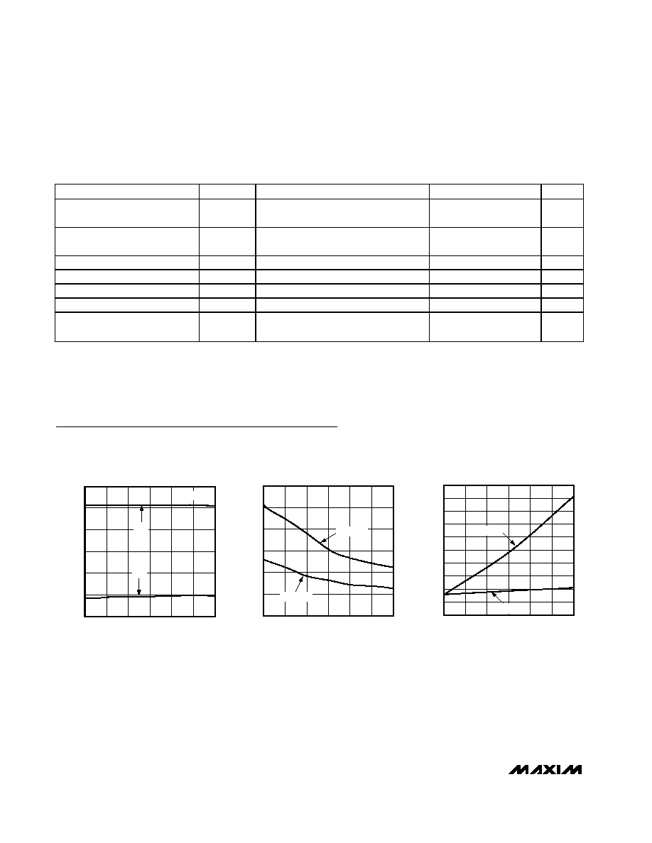
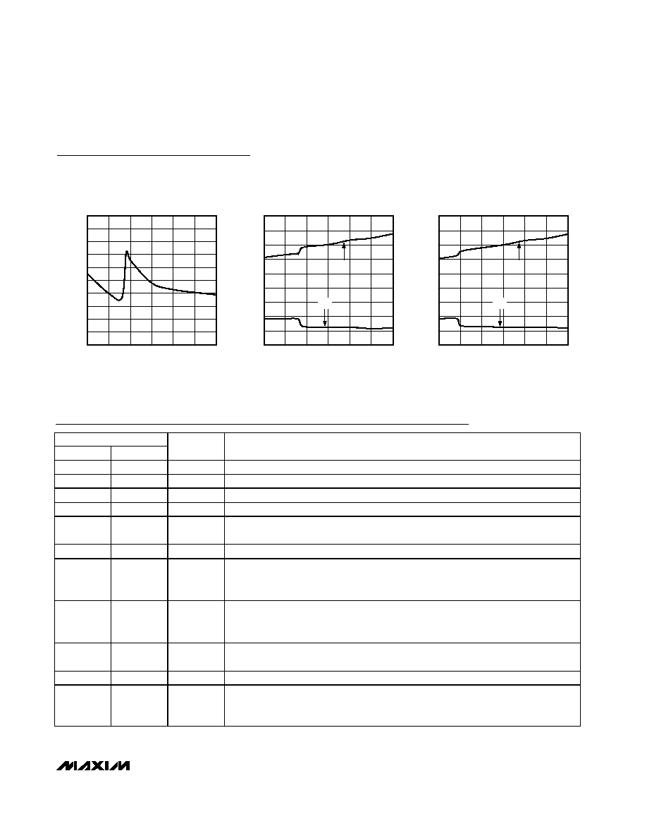
Typical Operating Characteristics
(V
CC
= +3.3V, 250kbps data rate, 0.1µF capacitors, all transmitters loaded with 3k and C
L
, T
A
= +25°C, unless otherwise noted.)
-6
-2
-4
2
0
4
6
0
1500
2000
500
1000
2500
3000
TRANSMITTER OUTPUT VOLTAGE
vs. LOAD CAPACITANCE
MAX3230/31E toc01
LOAD CAPACITANCE (pF)
TRANSMITTER OUTPUT VOLTAGE (V)
V
OH
V
OL
V
CC
RISING
0
10
5
20
15
25
30
0
2500
3000
SLEW RATE vs. LOAD CAPACITANCE
MAX3230/31E toc02
LOAD CAPACITANCE (pF)
SLEW RATE (V/
µ
s)
1000
500
1500
2000
V
CC
= 5.5V
V
CC
= 2.5V
0
6
4
2
8
10
12
14
16
18
20
0
1000
500
1500
2000
2500
3000
OPERATING SUPPLY CURRENT
vs. LOAD CAPACITANCE (MAX3231E)
MAX3230/31E toc03
LOAD CAPACITANCE (pF)
OPERATING SUPPLY CURRENT (mA)
250kbps
20kbps
MAX3230E/MAX3231E
±15kV ESD-Protected +2.5V to +5.5V
RS-232 Transceivers in UCSP
_______________________________________________________________________________________
5
BUMP
MAX3230E
MAX3231E
NAME
FUNCTION
A1
A1
V
CC
+2.5V to +5.5V Supply Voltage
A2
A2
C2+
Inverting Charge-Pump Capacitor Positive Terminal
A3
A3
C2-
Inverting Charge-Pump Capacitor Negative Terminal
A4
A4
V-
Negative Supply Voltage (-5.5V/-4.0V) Generated by Charge Pump
A5
A5
V
L
Logic Supply Input. Logic-level input for receiver outputs and transmitter inputs.
Connect V
L
to the system-logic supply voltage or V
CC
if no logic supply is required.
A6, B6
A6
T_IN
Transmitter Input(s)
B1
B1
V+
Positive Supply Voltage (+5.5V/+4.0V) Generated by Charge Pump. If charge pump is
generating +4.0V, the device has switched from RS-232-compliant to RS-232-
compatible mode.
B2, B3, B4,
C2, C3, C4,
D2D5
B2, B3, B4,
C2, C3, C4,
D2D5
N.C.
No Connection. These locations are not populated with solder bumps.
B5
B5
FORCEON
Active-High FORCEON Input. Drive FORCEON high to override automatic circuitry,
keeping transmitters and charge pumps on.
C1
C1
C1+
Positive Regulated Charge-Pump Capacitor Positive Terminal
C5
C5
FORCEOFF
Active-Low FORCEOFF Input. Drive FORCEOFF low to shut down transmitters,
receivers, and on-board charge pump. This overrides all automatic circuitry and
FORCEON.
Pin Description
Typical Operating Characteristics (continued)
(V
CC
= +3.3V, 250kbps data rate, 0.1µF capacitors, all transmitters loaded with 3k and C
L
, T
A
= +25°C, unless otherwise noted.)
0
6
4
2
8
10
12
14
16
18
20
2.5
3.5
3.0
4.0
4.5
5.0
5.5
OPERATING SUPPLY CURRENT
vs. SUPPLY VOLTAGE (MAX3231E)
MAX3230/31E toc04
SUPPLY VOLTAGE (V)
OPERATING SUPPLY CURRENT (mA)
-8
-4
-6
2
0
-2
8
6
4
10
2.5
3.5
3.0
4.0
4.5
5.0
5.5
TRANSMITTER OUTPUT VOLTAGE
vs. SUPPLY VOLTAGE (V
CC
RISING)
MAX3230/31E toc05
SUPPLY VOLTAGE (V)
TRANSMITTER OUTPUT VOLTAGE (V)
V
OH
V
OL
-8
-4
-6
2
0
-2
8
6
4
10
2.5
3.5
3.0
4.0
4.5
5.0
5.5
TRANSMITTER OUTPUT VOLTAGE
vs. SUPPLY VOLTAGE (V
CC
FALLING)
MAX3230/31E toc06
SUPPLY VOLTAGE (V)
TRANSMITTER OUTPUT VOLTAGE (V)
V
OH
V
OL