 | –≠–ª–µ–∫—Ç—Ä–æ–Ω–Ω—ã–π –∫–æ–º–ø–æ–Ω–µ–Ω—Ç: MAX3322E | –°–∫–∞—á–∞—Ç—å:  PDF PDF  ZIP ZIP |
General Description
The MAX3322E/MAX3323E 3.0V to 5.5V powered
EIA/TIA-232 and V.28/V.24 communications interfaces
are designed for multidrop applications with low power
requirements, high data-rate capabilities, and
enhanced electrostatic discharge (ESD) protection. All
RS-232 inputs and outputs are protected to ±15kV
using the IEC 1000-4-2 Air-Gap Discharge method,
±8kV using the IEC 1000-4-2 Contact Discharge
method, and ±15kV using the Human Body Model.
The MAX3322E/MAX3323E have pin-selectable
5k
/high-impedance RS-232 receivers. These devices
are capable of receiving data in high-impedance mode.
In multidrop applications, one receiver has a 5k
input
resistance, while the other receivers are high imped-
ance to ensure the RS-232 standard is observed. Logic
control permits selection of the functional mode: high
impedance or RS-232 standard load. The transmitters
are enabled by logic control to allow the multiplexing of
the inputs to a single UART.
A proprietary low-dropout transmitter output stage
enables true RS-232 performance from a 3.0V to 5.5V
supply with a dual charge pump. The charge pump
requires only four small 0.1µF capacitors for operation
from a 3.3V supply. The MAX3322E/MAX3323E are
capable of running at data rates up to 250kbps while
maintaining RS-232-compliant output levels. The
MAX3322E/MAX3323E have a unique V
L
pin that allows
operation in mixed-logic voltage systems. Both input
and output logic levels are pin programmable through
the V
L
pin.
The MAX3322E is a 2Tx/2Rx device for hardware hand-
shaking in standard RS-232 mode, and the MAX3323E
is a 1Tx/1Rx, required in most multidrop applications.
The MAX3322E is offered in a space-saving TSSOP
package. The MAX3323E is offered in 16-pin DIP and
space-saving TSSOP packages.
Applications
Bar-Code Scanners
Video Security
Industrial Data Acquisition
Data Splitters
Features
o Pin-Selectable 5k/High-Impedance Receivers
o Transmitter Outputs Three-Stated by Logic
Control
o V
L
Pin for Compatibility with Mixed Voltage
Systems
o 1Tx/1Rx (MAX3323E) or 2Tx/2Rx (MAX3322E)
Versions
o 250kbps Data Rate
o 1µA Low-Power Shutdown
o High ESD Protection for RS-232 I/O Pins
±15kV--Human Body Model
±8kV--IEC 1000-4-2 Contact Discharge
±15kV--IEC 1000-4-2 Air-Gap Discharge
MAX3322E/MAX3323E
±15kV ESD-Protected, RS-232 Transceivers for
Multidrop Applications
________________________________________________________________ Maxim Integrated Products
1
20
19
18
17
16
15
14
13
1
2
3
4
5
6
7
8
V
CC
GND
SHDN
V
L
C2+
C1-
V+
C1+
TOP VIEW
RENABLE
TXENABLE
TIN2
ROUT2
RIN2
TOUT2
V-
C2-
12
11
9
10
TIN1
ROUT1
RIN1
TOUT1
MAX3322E
TSSOP
Pin Configurations
Ordering Information
19-2667; Rev 1; 1/03
For pricing, delivery, and ordering information, please contact Maxim/Dallas Direct! at
1-888-629-4642, or visit Maxim's website at www.maxim-ic.com.
PART
TEMP RANGE
PIN-PACKAGE
MAX3322E EUP
-40
∞C to +85∞C
20 TSSOP
MAX3323E EUE
-40
∞C to +85∞C
16 TSSOP
MAX3323EEPE
-40
∞C to +85∞C
16 DIP
Pin Configurations continued at end of data sheet.
Typical Operating Circuit and Functional Diagram appear
at end of data sheet.

MAX3322E/MAX3323E
±15kV ESD-Protected, RS-232 Transceivers for
Multidrop Applications
2
_______________________________________________________________________________________
ABSOLUTE MAXIMUM RATINGS
Stresses beyond those listed under "Absolute Maximum Ratings" may cause permanent damage to the device. These are stress ratings only, and functional
operation of the device at these or any other conditions beyond those indicated in the operational sections of the specifications is not implied. Exposure to
absolute maximum rating conditions for extended periods may affect device reliability.
All Voltages Referenced to GND
V
CC
, V
L
....................................................................-0.3V to +6V
V+ (Note 1) ....................................................(V
CC
- 0.3V) to +7V
V- (Note 1) ................................................................+0.3V to -7V
V+ + |V-| (Note 1) .................................................................+13V
Input Voltages
TIN_, RENABLE, TXENABLE, SHDN .....................-0.3V to +6V
RIN_ ..................................................................................±25V
Output Voltages
TOUT_............................................................................±13.2V
ROUT_........................................................-0.3V to (V
L
+ 0.3V)
Short-Circuit Duration TOUT_ to GND........................Continuous
Continuous Power Dissipation (T
A
= +70∞C)
16-Pin DIP (derate 10.5mW/∞C above +70∞C) ............842mW
16-Pin TSSOP (derate 9.4mW/∞C above +70∞C) ........755mW
20-Pin TSSOP(derate 11mW/∞C above +70∞C) ..........879mW
Operating Temperature Range
MAX3322E/MAX3323E ...................................-40∞C to +85∞C
Junction Temperature ..................................................... +150∞C
Storage Temperature Range .............................-65∞C to +150∞C
Lead Temperature (soldering, 10s) .................................+300∞C
DC ELECTRICAL CHARACTERISTICS
(V
CC
= 3.0V to 5.5V, V
L
= 1.65V to 5.5V, C1≠C4 = 0.1µF, tested at +3.3V ±10%; C1 = 0.047µF, C2 = C3 = C4 = 0.33µF, tested at +5V
±10%; T
A
= T
MIN
to T
MAX
. Typical values are at V
CC
= V
L
= 3.3V and T
A
= +25∞C, unless otherwise noted.)
PARAMETER
SYMBOL
CONDITIONS
MIN
TYP
MAX
UNITS
DC CHARACTERISTICS
Supply Current Normal Operation
I
CC
SHDN = V
L
, no load
1
mA
Supply Current in Shutdown
I
CC(SHDN)
SHDN = 0V, no load
1
10
µA
TRANSMITTER LOGIC INPUTS
Input Logic Threshold Low
0.4
V
V
L
1.8V
V
L
- 0.4
Input Logic Threshold High
V
L
> 1.8V
2/3 x V
L
V
Transmitter Input Hysteresis
0.2
V
Input Leakage Current
I
IL
±0.01
±1
µA
LOGIC INPUTS (TXENABLE, RENABLE, SHDN)
Input Logic Threshold Low
0.4
V
Input Logic Threshold High
2/3 x V
L
V
Input Leakage Current
±0.01
±1
µA
RECEIVER OUTPUTS
Output Leakage Current
I
OL
Receivers disabled, SHDN = 0V
+
0.05
+ 10
µA
I
OUT
= 1.6mA, V
L
> 1.8V
0.4
Output Voltage Low
V
OL
I
OUT
= 1mA, V
L
1.8V
0.4
V
I
OUT
= -1mA, V
L
> 1.8V
V
L
- 0.4 V
L
- 0.1
Output Voltage High
V
OH
I
OUT
= -500µA, V
L
1.8V
V
L
- 0.4
V
L
- 0.1
V
RECEIVER INPUTS
Input Voltage Range
V
RIN
-25
+25
V
V
L
= 1.65V
0.25
0.6
V
L
= 3.3V
0.6
1.2
Input Threshold Low
V
L
= 5.0V
0.8
1.5
V
Note 1: V+ and V- can have maximum magnitudes of 7V, but their absolute difference cannot exceed 13V.
MAX3322E/MAX3323E
±15kV ESD-Protected, RS-232 Transceivers for
Multidrop Applications
_______________________________________________________________________________________
3
DC ELECTRICAL CHARACTERISTICS (continued)
(V
CC
= 3.0V to 5.5V, V
L
= 1.65V to 5.5V, C1≠C4 = 0.1µF, tested at +3.3V ±10%; C1 = 0.047µF, C2 = C3 = C4 = 0.33µF, tested at +5V
±10%; T
A
= T
MIN
to T
MAX
. Typical values are at V
CC
= V
L
= 3.3V and T
A
= +25∞C, unless otherwise noted.)
PARAMETER
SYMBOL
CONDITIONS
MIN
TYP
MAX
UNITS
V
L
= 1.65V
1
1.4
V
L
= 3.3V
1.5
2.4
Input Threshold High
V
L
= 5.0V
1.8
2.4
V
Input Hysteresis
0.35
V
RENABLE = 1
3
5
7
k
Input Resistance
R
IN
RENABLE = 0 or SHDN = 0V, R
IN
from -13V
to +13V
1
M
TRANSMITTER OUTPUTS
Output Voltage Swing
All transmitter outputs loaded with 3k
to
ground
±5
±5.4
V
Output Resistance
V
CC
= V+ = V- = 0, TOUT_ = ±2V,
TXENABLE = 1
300
10M
Output Short-Circuit Current
V
OUT
= 0V
±60
mA
Output Leakage Current
V
OUT
= ±12V, transmitters disabled
±25
µA
ESD PROTECTION
Human Body Model
±15
IEC 1000-4-2 Air-Gap Discharge
±15
RIN, TOUT
IEC 1000-4-2 Contact Discharge
±8
kV
TIMING CHARACTERISTICS
(V
CC
= 3.0V to 5.5V, V
L
= 1.65V to 5.5V, C1≠C4 = 0.1µF, tested at +3.3V ±10%; C1 = 0.047µF, C2 = C3 = C4 = 0.33µF, tested at +5V
±10%; T
A
= T
MIN
to T
MAX
. Typical values are at V
CC
= V
L
= 3.3V and T
A
= +25∞C, unless otherwise noted.)
PARAMETER
SYMBOL
CONDITIONS
MIN
TYP
MAX
UNITS
Maximum Data Rate
R
L
= 3k
, C
L
= 1000pF, one transmitter
switching
250
kbps
t
PHL
150
Receiver Propagation Delay
t
PLH
RIN_ to ROUT_, C
L
= 30pF, V
L
= 3.3V,
Figure 2
180
ns
t
PHL
0.6
Transmitter Propagation Delay
t
PLH
TIN _ to TO U T_, R
L
= 3k
, C
L
= 1000p F,
Fi g ur e 1
0.7
µs
Time to Enter Three-State on Tx
( N ote 2)
10
50
µs
Time to Exit Three-State on Tx
( N ote 2)
3
50
µs
Time to Enable Resistor
( N ote 2)
0.4
10
µs
Time to Disable Resistor
( N ote 2)
0.2
10
µs
Time to Enter Shutdown
50
µs
Time to Exit Shutdown
50
µs
Transmitter Skew
100
ns
Receiver Skew
30
ns
Transition Region Slew Rate
R
L
= 3k
to 7k, C
L
= 1000pF, measured
from +3V to -3V or vice versa
6
30
V/µs
Note 2: Guaranteed by design. Not production tested.
MAX3322E/MAX3323E
±15kV ESD-Protected, RS-232 Transceivers for
Multidrop Applications
4
_______________________________________________________________________________________
Typical Operating Characteristics
(V
CC
= 3.3V, V
L
= 3.3V, C1≠C4 = 0.1µF, T
A
= +25∞C.)
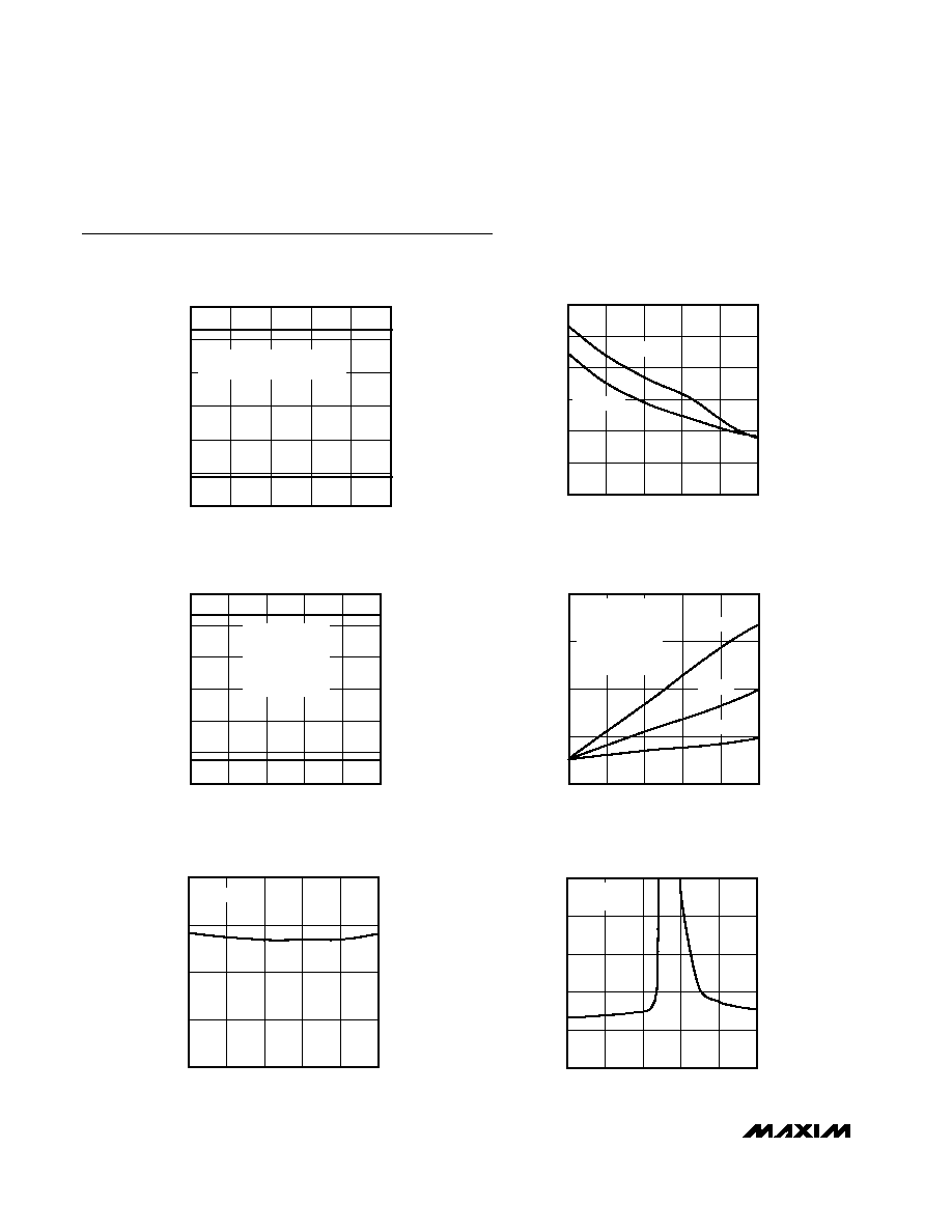
TRANSMITTER OUTPUT VOLTAGE
vs. LOAD CAPACITANCE
MAX3322E toc01
LOAD CAPACITANCE (pF)
OUTPUT VOLTAGE (V)
4000
3000
2000
1000
-5.0
-2.5
0
2.5
5.0
7.5
-7.5
0
5000
DATA RATE = 250kbps
LOAD = 3k
IN PARALLEL WITH C
L
SLEW RATE
vs. LOAD CAPACITANCE
MAX3322E toc02
LOAD CAPACITANCE (pF)
SLEW RATE (V/
µ
s)
4000
3000
2000
1000
3
6
9
12
15
18
0
0
5000
SLEW RATE-
SLEW RATE+
TRANSMITTER OUTPUT VOLTAGE
vs. DATA RATE
MAX3322E toc03
DATA RATE (kbps)
OUTPUT VOLTAGE (V)
200
150
100
50
-5.0
-2.5
0
2.5
5.0
7.5
-7.5
0
250
LOAD = 3k
, 1000pF
ONE TRANSMITTER
SWITCHING AT DATA
RATE, OTHER
TRANSMITTER
AT 1/8 DATA RATE
SUPPLY CURRENT
vs. LOAD CAPACITANCE
MAX3322E toc04
LOAD CAPACITANCE (pF)
SUPPLY CURRENT (mA)
4000
3000
2000
1000
10
20
30
40
0
0
5000
250kbps
125kbps
40kbps
LOAD = 3k
ONE TRANSMITTER
SWITCHING AT DATA
RATE, OTHER
TRANSMITTER
AT 1/8 DATA RATE
RECEIVER INPUT RESISTANCE
vs. INPUT VOLTAGE RANGE
MAX3322E toc05
V
RIN
(V)
RECEIVER INPUT RESISTANCE (k
)
15
5
-5
-15
4.75
5.00
5.25
5.50
4.50
-25
25
RENABLE = 1
RECEIVER INPUT RESISTANCE
vs. INPUT VOLTAGE RANGE
MAX3322E toc06
V
RIN
(V)
RECEIVER INPUT RESISTANCE (M
)
15
5
-5
-15
1
2
3
4
5
0
-25
25
RENABLE = 0
V
L
= 5V

Detailed Description
The MAX3322E/MAX3323E are RS-232 transceivers for
multidrop applications (i.e., multiple-receiver operation).
The devices are pin selectable between standard RS-232
operation with 5k
input resistance receivers or high-
input-impedance receivers. Receivers of the MAX3322E/
MAX3323E remain active in both modes of operation. In
multidrop applications, a selected receiver is set at a 5k
input resistance, while the others are high-input imped-
ance, maintaining RS-232 standards. Logic control per-
mits selection of the functional mode: high impedance or
normal load. The transmitters are enabled by logic control
to allow transmission-line sharing.
The logic supply input (V
L
) controls the levels of the
system's I/O and works from 1.65V to 5.5V, providing
compatibility with lower microprocessor I/O voltages.
The transmitters are inverting level translators that con-
vert CMOS logic levels into RS-232-compatible levels.
They guarantee 250kbps with loads of R
L
= 3k
and C
L
= 1000pF. The transmitters are enabled or disabled
(three-stated) by the logic control TXENABLE, which
manages transmission-line sharing in multidrop applica-
tions. When TXENABLE is high, the transmitter is
enabled. When TXENABLE is low, the transmitter is put
in high-impedance state. The receivers can be used in
two conditions, selectable by the logic control RENABLE.
When RENABLE is high, the internal 5k
resistor is con-
nected across receiver input and ground. When
RENABLE is low, the receiver input is high impedance,
while maintaining receiving capability.
In shutdown mode, all transmitter and receiver outputs
are three-stated, receiver inputs are in high impedance,
the charge pump is turned off, V+ decays to V
CC
, and
V- decays to ground. ESD protection structures are
incorporated in all pins to protect against ESD events
encountered during handling and assembly. The
receiver inputs and the transmitter outputs have ±15kV
ESD structure implementation.
MAX3322E/MAX3323E
±15kV ESD-Protected, RS-232 Transceivers for
Multidrop Applications
_______________________________________________________________________________________
5
Pin Description
PIN
MAX3322E
MAX3323E
NAME
FUNCTION
1
1
C1+
Positive Terminal of the Voltage-Doubler Charge-Pump Capacitor
2
2
V+
+5.5V Generated by the Charge Pump
3
3
C1-
Negative Terminal of the Voltage-Doubler Charge-Pump Capacitor
4
4
C2+
Positive Terminal of the Inverting Charge-Pump Capacitor
5
5
C2-
Negative Terminal of the Inverting Charge-Pump Capacitor
6
6
V-
-5.5V Generated by the Charge Pump
7, 9
7
TOUT_
Transmitter Output
8, 10
8
RIN_
Receiver Input
11, 13
9
ROUT_
Receiver Output
12, 14
10
TIN_
Transmitter Input
15
11
TXENABLE
Transmitter Enable. Drive TXENABLE high to enable transmitter. Drive TXENABLE low
to put transmitter into high impedance.
16
12
RENABLE
Receiver Termination Enable. Drive RENABLE high for normal RS-232 5k
termination.
Drive RENABLE low to make receiver inputs high impedance. In either case, the
receiver and its output are enabled.
17
13
V
L
Logic-Level Supply. All CMOS inputs and outputs are referred to V
L
, which is from
1.65V to 5.5V.
18
14
SHDN
Shutdown Input. Drive SHDN low to put device into shutdown mode. Drive SHDN high
for normal operation. In shutdown, all transmitter and receiver outputs are in three-state;
receiver inputs are high impedance.
19
15
GND
Ground
20
16
V
CC
+3V to +5.5V Input Voltage. Bypass V
CC
to GND with a 0.1µF capacitor.