 | –≠–ª–µ–∫—Ç—Ä–æ–Ω–Ω—ã–π –∫–æ–º–ø–æ–Ω–µ–Ω—Ç: MAX3355E | –°–∫–∞—á–∞—Ç—å:  PDF PDF  ZIP ZIP |

General Description
The MAX3355E integrates a charge pump and com-
parators to enable a system with an integrated USB on-
the-go (OTG) dual-role transceiver to function as a USB
OTG dual-role device. USB OTG facilitates the direct
connection of peripherals and mobile devices such as
PDAs, cellular phones, MP3 players, and digital cam-
eras to one another without a host PC.
The MAX3355E's internal charge pump supplies V
BUS
power and signaling that is required by the transceiver as
defined in On-the-Go Supplement to the USB 2.0
Specification, Revision 1.0. The MAX3355E features ID
detection and internal comparators for monitoring
V
BUS
. The V
BUS
status outputs are used during negoti-
ation for the USB according to the session request pro-
tocol (SRP) and host negotiation protocol (HNP).
The MAX3355E operates with logic supply voltages
(V
L
) as low as 1.65V, ensuring compatibility with low-
voltage ASICs. The device also features a logic-selec-
table 1µA shutdown mode.
The MAX3355E has built-in ±15kV ESD-protection cir-
cuitry to protect the V
BUS
and ID_IN pins. The device is
available in a miniature 4 x 3 chip-scale package
(UCSP), as well as a 14-pin TSSOP package, and is
specified for operation over the -40∞C to +85∞C extended
temperature range.
Applications
Cell Phones
MP3 Players
PDAs
Digital Cameras
Features
o Guaranteed 8mA (min) V
BUS
Charge-Pump Output
o ±15kV ESD Protection on V
BUS
and ID_IN
o Up to +6.0V Backdrive Capability for V
BUS
o +2.6V to +5.5V Operating Voltage Range
o V
L
Operates Down to +1.65V
o Guaranteed V
BUS
Input Impedance When Not
Driven
o Automatic C
LOAD
Detection
o Comparators for Host Negotiation Protocol
o ID_IN Detection
o Available in 4 x 3 UCSP or 14-Pin TSSOP Package
MAX3355E
±15kV ESD-Protected USB On-the-Go
Charge Pump and Comparators in UCSP
________________________________________________________________ Maxim Integrated Products
1
PART
TEMP RANGE
PIN-
PACKAGE
TOP
MARK
MAX3355EEBC-T
-40∞C to +85∞C
4 x 3 UCSP
ABE
MAX3355EEUD
-40∞C to +85∞C
14 TSSOP
--
Ordering Information
CHARGE
PUMP
5V AT 8mA
40k
TO
100k
STATUS2
STATUS1
ON/OFF
MAX3355E
V
BUS
COMPARATORS
CURRENT
SOURCE
V
BUS
V
BUS
GND
USB CONNECTOR
ID_IN
GND
ID
D+
D-
V
CC
V
L
C+
V
CC
C-
ESD
LEVEL
SHIFTER
OFFVBUS
SHDN
STATUS1
STATUS2
ID_OUT
DUAL-ROLE
ASIC
LOGIC SUPPLY
+1.65V TO V
CC
USB
XCVR
ESD
Functional Diagram
19-2844; Rev 1; 8/03
For pricing, delivery, and ordering information, please contact Maxim/Dallas Direct! at
1-888-629-4642, or visit Maxim's website at www.maxim-ic.com.
Pin Configurations appear at end of data sheet.
MAX3355E
±15kV ESD-Protected USB On-the-Go
Charge Pump and Comparators in UCSP
2
_______________________________________________________________________________________
ABSOLUTE MAXIMUM RATINGS
ELECTRICAL CHARACTERISTICS
(V
CC
= +2.6V to +5.5V, V
L
= +1.65V to V
CC
, C1 = 0.1µF, V
CC
decoupled with 1µF capacitor to GND, V
L
decoupled with 0.1µF
capacitor to GND, C
LOAD
= 1µF (min), ESR
LOAD
= 1
(max), T
A
= T
MIN
to T
MAX
. Typical values are at V
CC
= +3.0V, V
L
= 1.8V, T
A
=
+25∞C, unless otherwise noted.) (Notes 1, 2)
Stresses beyond those listed under "Absolute Maximum Ratings" may cause permanent damage to the device. These are stress ratings only, and functional
operation of the device at these or any other conditions beyond those indicated in the operational sections of the specifications is not implied. Exposure to
absolute maximum rating conditions for extended periods may affect device reliability.
(All voltages referenced to GND)
V
CC
, V
L
, V
BUS
, ID_IN.............................................-0.3V to +6.0V
C+..................................................................(V
CC
- 0.3V) to +6V
C-................................................................-0.3V to (V
CC
+ 0.3V)
OFFVBUS, SHDN, STATUS1,
STATUS2, ID_OUT ....................................-0.3V to (V
L
+ 0.3V)
V
BUS
Short Circuit to GND .........................................Continuous
Output Current (all other pins)..........................................±15mA
Continuous Power Dissipation (T
A
= +70∞C)
4 x 3 UCSP (derate 6.5mW/∞C above +70∞C) .............520mW
14-Pin TSSOP (derate 9.1mW/∞C above +70∞C) .........727mW
Operating Temperature Range ...........................-40∞C to +85∞C
Storage Temperature Range .............................-65∞C to +150∞C
Junction Temperature ......................................................+150∞C
Lead Temperature (soldering, 10s) .................................+300∞C
Bump Temperature (soldering)
Infrared (15s) ...............................................................+200∞C
Vapor Phase (20s) .......................................................+215∞C
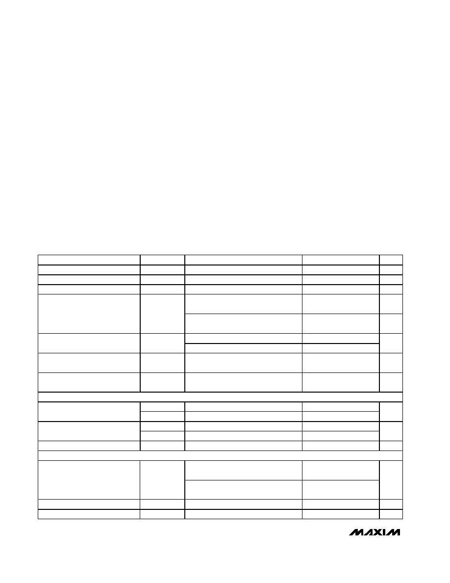
PARAMETER
SYMBOL
CONDITIONS
MIN
TYP
MAX
UNITS
Supply Voltage
V
CC
2.6
5.5
V
Logic Supply Voltage
V
L
1.65
V
CC
V
Logic Supply Current
I
L
100
µA
No activity on V
BUS
; comparator and
reference active
200
µA
Operating Supply Current
I
CC
Device A configured,
OFFVBUS = V
L
,
I
LOAD
= 8mA, charge pump on
20
mA
Device B configured,
SHDN = GND
1
Shutdown Supply Current
I
CC
SHDN
Device A configured,
SHDN = GND
30
µA
Thermal-Shutdown Protection
Threshold
Device A configured,
OFFVBUS = V
L
,
charge pump on
+150
∞C
Thermal-Shutdown Protection
Hysteresis
Device A configured,
OFFVBUS = V
L
,
charge pump on
+20
∞C
LOGIC INPUTS AND OUTPUTS
V
OH
I
SOURCE
= +1mA
2/3 x V
L
STATUS1, STATUS2, ID_OUT
Output Voltage
V
OL
I
SINK
= -1mA
0.4
V
V
IH
2/3 x V
L
OFFVBUS, SHDN Input Voltage
V
IL
0.4
V
Input Leakage Current
I
LKG
OFFVBUS, SHDN = GND or V
L
±1
µA
V
BUS
OUTPUT VOLTAGE: DEVICE A CONFIGURED
I
LOAD
= 0 to 8mA, C
LOAD
= 1µF,
OFFVBUS = V
L
, ID_IN = GND
4.63
5.25
V
BUS
Output Voltage
No load, C
LOAD
= 1µF,
OFFVBUS = V
L
,
ID_IN = GND
4.8
V
V
BUS
Leakage Voltage
OFFVBUS = GND
200
mV
V
BUS
Sink Current
OFFVBUS = GND, V
BUS
= +6.0V
150
µA

MAX3355E
±15kV ESD-Protected USB On-the-Go
Charge Pump and Comparators in UCSP
_______________________________________________________________________________________
3
ELECTRICAL CHARACTERISTICS (continued)
(V
CC
= +2.6V to +5.5V, V
L
= +1.65V to V
CC
, C1 = 0.1µF, V
CC
decoupled with 1µF capacitor to GND, V
L
decoupled with 0.1µF
capacitor to GND, C
LOAD
= 1µF (min), ESR
LOAD
= 1
(max), T
A
= T
MIN
to T
MAX
. Typical values are at V
CC
= +3.0V, V
L
= 1.8V, T
A
=
+25∞C, unless otherwise noted.) (Notes 1, 2)
PARAMETER
SYMBOL
CONDITIONS
MIN
TYP
MAX
UNITS
V
BUS
Source Current
OFFVBUS = V
L,
ID_IN = GND
8
mA
V
BUS
Short-Circuit Current Limit
V
BUS
shorted to GND
200
mA
V
BUS
Output Ripple
I
LOAD
= 8mA, C
LOAD
= 1µF,
OFFVBUS = V
L
, ID_IN = GND (Note 3)
100
mV
Charge-Pump Switching
Frequency
500
kHz
V
BUS
Input Impedance
R
INVBUS
OFFVBUS = GND or SHDN = GND
40
100
k
LOAD DETECTION V
BUS
OUTPUT VOLTAGE
C
LOAD
= 20µF,
OFFVBUS = V
L
, ID_IN =
V
CC
, I
BUS
source on-time = t
VBUSCHRG
2.1
V
BUS
Output Voltage
C
LOAD
= 95µF,
OFFVBUS = V
L
, ID_IN =
V
CC
, I
BUS
source on-time = t
VBUSCHRG
1.9
V
V
BUS
Source Current
OFFVBUS = V
L
,
ID_IN = V
CC
(Note 4)
450
600
850
µA
V
BUS
Current Gate Time
t
VBUSCHRG
OFFVBUS = V
L
, ID_IN = V
CC
, Device B
(Note 4)
155
(max)
105
56
(min)
ms
V
BUS
COMPARATOR
V
BUS
Valid Comparator Threshold
V
THVBUSVLD
V
BUS
rising
4.4
4.55
4.63
V
V
BUS
Valid Comparator Hysteresis
20
mV
Session Valid Comparator
Threshold
V
THSESVLD
1.12
1.4
1.68
V
Session Valid Comparator
Hysteresis
15
mV
B-Session End Comparator
Threshold
V
THSESEND
0.4
0.5
0.6
V
B-Session End Comparator
Hysteresis
30
mV
Shutdown Comparator
V
TH,
SHDN
0.8
2.4
V
ID_IN
ID_IN Voltage Input for Device B
2/3 x V
cc
V
ID_IN Voltage Input for Device A
0.4
V
ID_IN Input Impedance
150
200
250
k
ESD PROTECTION (ID_IN, V
BUS
)
Human Body Model
±15
kV
IFC 1000-4-2 Air-Gap Discharge
±15
kV
IFC 1000-4-2 Contact Discharge
±8
kV

MAX3355E
±15kV ESD-Protected USB On-the-Go
Charge Pump and Comparators in UCSP
4
_______________________________________________________________________________________
Typical Operating Characteristics
(V
CC
, V
L
= +3.3V, C1 = 0.1µF, V
CC
decoupled with 1µF capacitor to GND, V
L
decoupled with 0.1µF capacitor to GND, C
LOAD
= 1µF
min, ESR
LOAD
= 1
max, T
A
= +25∞C, unless otherwise noted.)
0
40
20
80
60
100
120
0
50
V
CC
INPUT CURRENT
vs. V
BUS
OUTPUT CURRENT
MAX3355E toc01
V
BUS
OUTPUT CURRENT (mA)
V
CC
INPUT CURRENT (mA)
20
10
30
40
V
CC
= 2.6V
V
CC
= 4.0V
V
CC
= 5.5V
4.00
4.50
4.25
4.75
5.00
5.25
0
50
V
BUS
OUTPUT VOLTAGE
vs. V
BUS
OUTPUT CURRENT
MAX3355E toc02
V
BUS
OUTPUT CURRENT (mA)
V
BUS
OUTPUT VOLTAGE (V)
20
10
30
40
V
CC
= 4.0V
V
CC
= 5.5V
V
CC
= 2.6V
0
75
25
50
100
125
150
2.5
5.5
V
BUS
OUTPUT RIPPLE VOLTAGE
vs. V
CC
INPUT VOLTAGE
MAX3355E toc03
V
CC
INPUT VOLTAGE (V)
V
BUS
OUTPUT RIPPLE VOLTAGE (mV)
3.5
3.0
4.0
5.0
4.5
I
VBUS
= 8mA
TIMING CHARACTERISTICS
(V
CC
= +2.6V to +5.5V, V
L
= +1.65V to V
CC
, C1 = 0.1µF, V
CC
decoupled with 1µF capacitor to GND, V
L
decoupled with 0.1µF
capacitor to GND, C
LOAD
= 1µF (min), ESR
LOAD
= 1
(max), T
A
= T
MIN
to T
MAX
. Typical values are at V
CC
= +3.0V, V
L
= 1.8V, T
A
=
+25∞C, unless otherwise noted.) (Notes 1, 2)
PARAMETER
SYMBOL
CONDITIONS
MIN
TYP
MAX
UNITS
V
BUS
Rise Time
0 to 4.4V, C
LOAD
= 1µF, I
LOAD
= 8mA
100
ms
OFFVBUS Propagation Delay
6
µs
Comparator Propagation Delay
3
µs
Time to Exit Shutdown
50
µs
Time to Shutdown
1
µs
ID_OUT Rise Time
C
ID_OUT
= 50pF
10
ns
ID_OUT Fall Time
C
ID_OUT
= 50pF
10
ns
Note 1: Limits are 100% production tested at +25∞C. Limits over temperature are guaranteed by design.
Note 2: All currents out of the device are positive; all currents into the device are negative. All voltages are referenced to device
ground unless otherwise specified.
Note 3: The ripple voltage is strongly correlated to the bus capacitance and its ESR.
Note 4: The V
BUS
current source and current gate time vary together with process and temperature such that the resulting V
BUS
pulse is guaranteed to drive a <13µF load to a voltage >2.0V, and to drive a >96µF load to a voltage <2.2V.

MAX3355E
±15kV ESD-Protected USB On-the-Go
Charge Pump and Comparators in UCSP
_______________________________________________________________________________________
5
Typical Operating Characteristics (continued)
(V
CC
, V
L
= +3.3V, C1 = 0.1µF, V
CC
decoupled with 1µF capacitor to GND, V
L
decoupled with 0.1µF capacitor to GND, C
LOAD
= 1µF
min, ESR
LOAD
= 1
max, T
A
= +25∞C, unless otherwise noted.)
4.0
4.8
4.2
4.4
4.6
5.0
5.2
5.4
2.5
5.5
V
BUS
OUTPUT VOLTAGE
vs. V
CC
INPUT VOLTAGE
MAX3355E toc04
V
CC
INPUT VOLTAGE (V)
V
BUS
OUTPUT VOLTAGE (V)
3.5
3.0
4.0
5.0
4.5
I
VBUS
= 0mA
I
VBUS
= 8mA
65
67
66
68
69
70
-40
85
V
BUS
INPUT IMPEDANCE
vs. TEMPERATURE
MAX3355E toc05
TEMPERATURE (
∞C)
V
BUS
INPUT IMPEDANCE (k
)
10
-15
35
60
16
17
18
19
20
-40
85
SUPPLY CURRENT
vs. TEMPERATURE
MAX3355E toc06
TEMPERATURE (
∞C)
SUPPLY CURRENT (mA)
10
-15
35
60
I
VBUS
= 8mA
V
CC
= 4.0V
V
CC
= 2.6V
V
CC
= 5.5V
V
BUS
vs. CAPACITANCE LOAD
DURING LOAD DETECTION
MAX3355E toc07
C
VBUS
= 10
µF
1V/div
C
VBUS
= 96
µF
1V/div
40ms/div
0
0