 | ÐлекÑÑоннÑй компоненÑ: MAX3381E | СкаÑаÑÑ:  PDF PDF  ZIP ZIP |
Äîêóìåíòàöèÿ è îïèñàíèÿ www.docs.chipfind.ru
General Description
The MAX3380E/MAX3381E are +2.35V to +5.5V-pow-
ered EIA/TIA-232 and V.28/V.24 communication inter-
faces with low power requirements, high data-rate
capabilities, and enhanced electrostatic discharge
(ESD) protection on both the TTL and RS-232 sides.
The MAX3380E/MAX3381E have two receivers and two
transmitters. All RS-232 inputs, outputs, and logic input
pins are protected to ±15kV using IEC 1000-4-2 Air-
Gap Discharge method and the Human Body Model,
and ±8kV using IEC 1000-4-2 Contact Discharge
method.
The proprietary low-dropout transmitter output stage
enables true RS-232 performance from a +3.1V to
+5.5V supply with a dual charge pump. The parts
reduce the transmitter output levels to RS-232-compati-
ble levels with no increase in supply current for sup-
plies less than +3.1V and greater than +2.35V. The
+2.35V to +5.5V operating range is fully compatible
with lithium-ion (Li+) batteries. The charge pump
requires only four small 0.1µF capacitors for operation.
The MAX3380E/MAX3381E transceivers use Maxim's
revolutionary AutoShutdown PlusTM feature to auto-
m a t i c a l l y e n t e r a 1 µ A s h u t d o w n m o d e . T h e s e
devices shut down the on-board power supply and
drivers when they do not sense a valid signal transi-
tion for 30 seconds on either the receiver or trans-
mitter inputs.
The MAX3380E is capable of transmitting data at
rates of 460kbps while maintaining RS-232 output
levels, and the MAX3381E operates at data rates up
to 250kbps. The MAX3381E offers a slower slew rate
for applications where noise and EMI are issues. The
MAX3380E/MAX3381E have a unique V
L
pin that
allows interoperation in mixed-logic voltage systems
down to +1.65V. Both input and output logic levels
are referenced to the V
L
pin. The MAX3380E/MAX3381E
are available in a space-saving TSSOP package.
Applications
Cell Phone Data Lump Cables
PDA Data Lump Cables
GPS Receivers
Digital Cameras
Features
o ±15kV ESD Protection on All CMOS and RS-232
Inputs and Outputs (Except INVALID)
±15kV Human Body Model
±15kV IEC 1000-4-2 Air-Gap Discharge
±8kV IEC 1000-4-2 Contact Discharge
o Operates Over Entire Li+ Battery Range
o Low Logic Threshold Down to +1.65V for
Compatibility with Cell Phone Logic Supply Voltages
o 1µA Low-Power AutoShutdown Plus Mode
o Compatible with Next-Generation GSM Data Rates
o 20-Pin TSSOP Package
MAX3380E/MAX3381E
+2.35V to +5.5V, 1µA, 2Tx/2Rx RS-232 Transceivers
with ±15kV ESD-Protected I/O and Logic Pins
________________________________________________________________ Maxim Integrated Products
1
19-2128; Rev 0; 8/01
Ordering Information
PART
TEMP. RANGE
PIN-PACKAGE
MAX3380ECUP
0
°C to +70°C
20 TSSOP
MAX3380EEUP
-40
°C to +85°C
20 TSSOP
MAX3381ECUP
0
°C to +70°C
20 TSSOP
MAX3381EEUP
-40
°C to +85°C
20 TSSOP
Pin Configuration appears at end of data sheet.
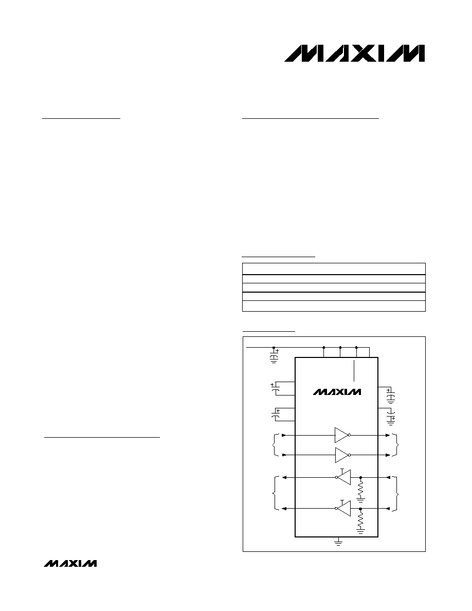
MAX3380E/
MAX3381E
R2OUT
R1OUT
R2IN
GND
RS-232
OUTPUTS
TTL/CMOS
INPUTS
T2IN
T1IN
C2-
C2+
C1-
C1+
R1IN
T2OUT
T1OUT
V-
V+
V
CC
V
L
C1
0.1
µF
C2
0.1
µF
C5
0.1
µF
+3.3V
RS-232
INPUTS
TTL/CMOS
OUTPUTS
5k
5k
C3
0.1
µF
C4
0.1
µF
V
L
V
L
FORCEON
FORCEOFF
Typical Operating Circuit
For pricing, delivery, and ordering information, please contact Maxim/Dallas Direct! at
1-888-629-4642, or visit Maxim's website at www.maxim-ic.com.
AutoShutdown Plus is a trademark of Maxim Integrated Products
MAX3380E/MAX3381E
+2.35V to +5.5V, 1µA, 2Tx/2Rx RS-232 Transceivers
with ±15kV ESD-Protected I/O and Logic Pins
2
_______________________________________________________________________________________
ABSOLUTE MAXIMUM RATINGS
ELECTRICAL CHARACTERISTICS
(V
CC
= +2.35V to +5.5V, V
L
= +1.65V to +5.5V. When V
CC
< +4.5V, C1 = C2 = C3 = C4 = 0.1µF; when V
CC
+4.5V, C1 = 0.047µF,
C2 = C3 = C4 = 0.33µF; T
A
= T
MIN
to T
MAX
, unless otherwise noted. Typical values are at V
CC
= V
L
= +3.3V, T
A
= +25°C.)
Stresses beyond those listed under "Absolute Maximum Ratings" may cause permanent damage to the device. These are stress ratings only, and functional
operation of the device at these or any other conditions beyond those indicated in the operational sections of the specifications is not implied. Exposure to
absolute maximum rating conditions for extended periods may affect device reliability.
Note 1: V+ and V- can have maximum magnitudes of +7V, but their absolute difference cannot exceed +13V.
V
CC
to GND ...........................................................-0.3V to +6.0V
V
L
to GND..............................................................-0.3V to +6.0V
V+ to GND .............................................................-0.3V to +7.0V
V- to GND ..............................................................+0.3V to -7.0V
V+ + |V-| (Note 1) .................................................................+13V
Input Voltages
T_IN, FORCEON, FORCEOFF to GND ...............-0.3V to +6.0V
R_IN to GND .....................................................................±25V
Output Voltages
T_OUT to GND...............................................................±13.2V
R_OUT, INVALID to GND ...........................-0.3V to (V
L
+ 0.3V)
Short-Circuit Duration T_OUT to GND........................Continuous
Continuous Power Dissipation (T
A
= +70°C)
20-Pin TSSOP (derate 10.9mW/°C over +70°C) .........879mW
Operating Temperature Ranges
MAX3380ECUP/MAX3381ECUP........................0°C to +70°C
MAX3380EEUP/MAX3381EEUP .....................-40°C to +85°C
Junction Temperature ......................................................+150°C
Storage Temperature Range .............................-65°C to +150°C
Lead Temperature (soldering, 10s) .................................+300°C
PARAMETER
SYMBOL
CONDITIONS
MIN
TYP
MAX
UNITS
Receivers idle, V
T
_
IN
= V
CC
or GND,
FORCEON = GND,
FORCEOFF = V
CC
10
Supply Current, AutoShutdown
Plus
I
CC
FORCEOFF = GND
1
10
µA
Supply Current, Normal Operation
I
CC
FORCEON =
FORCEOFF = V
L
, no load
0.3
1
mA
LOGIC INPUTS (T_IN, FORCEON, FORCEOFF)
V
CC
= +5.5V, V
L
= +5.5V
0.4
1.2
Input Logic Threshold Low
V
IL
V
CC
= +2.5V, V
L
= +1.65V
0.4
V
V
CC
= +5.5V, V
L
= +5.5V
V
L
0.66
Input Logic Threshold High
V
IH
V
CC
= +2.5V, V
L
= +1.65V
V
L
0.66
V
Transmitter Input Hysteresis
0.5
V
Input Leakage Current
±0.01
±1
µA
RECEIVER OUTPUTS (R_OUT) AND INVALID
Output Voltage Low
I
OUT
= 500µA
0.5
V
Output Voltage High
I
OUT
= -500µA
V
L
- 0.4 V
L
- 0.2
V
RECEIVER INPUTS (R_IN)
Input Voltage Range
-25
+25
V
V
L
= +3.3V
0.6
1.2
Input Threshold Low
T
A
= +25
°C
V
L
= +5.0V
0.8
1.5
V
V
L
= +3.3V
1.5
2.4
Input Threshold High
T
A
= +25
°C
V
L
= +5.0V
1.8
2.4
V
Input Hysteresis
0.3
V
Input Resistance
T
A
= +25°C
3
5
7
k
MAX3380E/MAX3381E
+2.35V to +5.5V, 1µA, 2Tx/2Rx RS-232 Transceivers
with ±15kV ESD-Protected I/O and Logic Pins
_______________________________________________________________________________________
3
PARAMETER
SYMBOL
CONDITIONS
MIN
TYP
MAX
UNITS
AutoShutdown Plus (FORCEON = GND, FORCEOFF = VL)
Positive threshold
2.7
Receiver Input Threshold to
INVALID Output High
Figure 3
Negative threshold
-2.7
V
Receiver Input Threshold to
INVALID Output Low
Figure 3
-0.3
0.3
V
Receiver Positive or Negative
Threshold to
INVALID High
t
INVL
V
CC
= +5.0V, Figure 4
0.3
µs
Receiver Positive or Negative
Threshold to
INVALID Low
t
INVH
V
CC
= +5.0V, Figure 4
30
µs
Receiver or Transmitter Edge to
Transmitters Enabled
t
WU
V
CC
= +5.0V, Figure 4
15
µs
Receiver or Transmitter Edge to
Transmitters Shutdown
t
AU T OS H D N
V
CC
= +5.0V, Figure 4
30
s
TRANSMITTER OUTPUTS
V
CC
Mode Switch Point
(V
CC
Falling)
T_OUT =
±5.0V to ±3.7V
2.95
3.1
3.25
V
V
CC
Mode Switch Point
(V
CC
Rising)
T_OUT =
±3.7V to ±5.5V
3.3
3.5
3.7
V
V
CC
Mode Switch Point
Hysteresis
400
mV
V
C C
= + 3.25V to + 5.5V ,
V
C C
fal l i ng
±5
±5.4
Output Voltage Swing
All transmitter
outputs loaded
with 3k
to ground V
C C
= + 2.5V to + 2.95V ,
V
C C
fal l i ng
±3.7
V
Output Resistance
V
CC
= 0, transmitter output =
±2.0V
300
10M
Output Short-Circuit Current
±60
mA
Output Leakage Current
V
OUT
=
±12V, transmitters disabled
±25
µA
ESD PROTECTION
Human Body Model
±15
IEC 1000-4-2 Air-Gap Discharge Method
±15
R_IN, T_OUT, R_OUT, T_IN,
FORCEON,
FORCEOFF
IEC 1000-4-2 Contact Discharge Method
±8
kV
ELECTRICAL CHARACTERISTICS (continued)
(V
CC
= +2.35V to +5.5V, V
L
= +1.65V to +5.5V. When V
CC
< +4.5V, C1 = C2 = C3 = C4 = 0.1µF; when V
CC
+4.5V, C1 = 0.047µF,
C2 = C3 = C4 = 0.33µF; T
A
= T
MIN
to T
MAX
, unless otherwise noted. Typical values are at V
CC
= V
L
= +3.3V, T
A
= +25°C.)
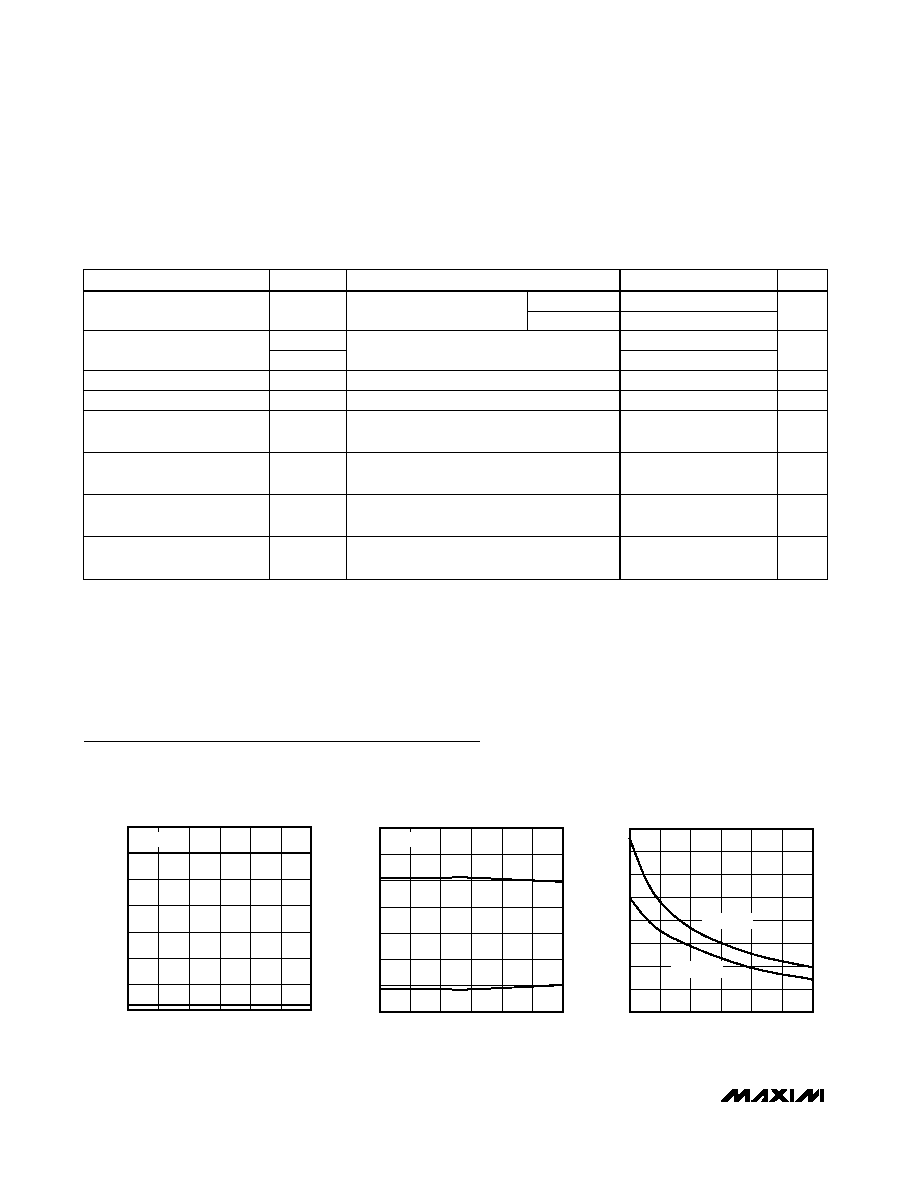
-6
-2
-4
2
0
6
4
8
0
1000
1500
500
2000
2500
3000
TRANSMITTER OUTPUT VOLTAGE
vs. LOAD CAPACITANCE
MAX3380E toc01
LOAD CAPACITANCE (pF)
TRANSMITTER OUTPUT VOLTAGE (V)
V
OUT+
V
OUT-
V
CC
= +4.2V
-6
-2
-4
2
0
6
4
8
0
1000
1500
500
2000
2500
3000
TRANSMITTER OUTPUT VOLTAGE
vs. LOAD CAPACITANCE
MAX3380E toc02
LOAD CAPACITANCE (pF)
TRANSMITTER OUTPUT VOLTAGE (V)
V
OUT+
V
OUT-
V
CC
= +2.5V
0
5
10
15
20
25
30
35
40
0
1000
500
1500
2000
2500
3000
MAX3380E
SLEW RATE vs. LOAD CAPACITANCE
MAX3380E toc03
LOAD CAPACITANCE (pF)
SLEW RATE (V/
µ
s)
V
CC
= +4.2V
V
CC
= +2.5V
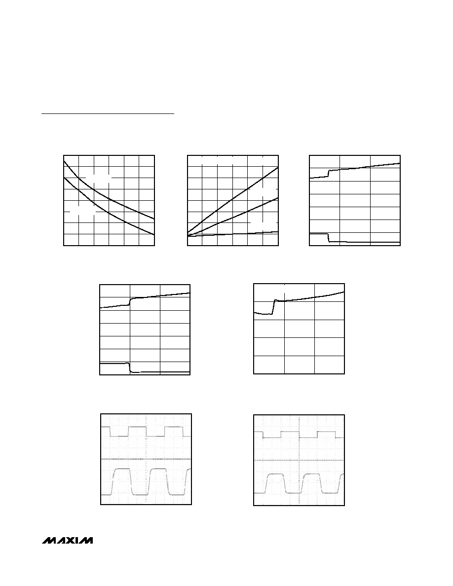
Typical Operating Characteristics
(V
CC
= V
L
= +4.2V, C1 = 0.22µF, C2 = C3 = C4 = 1µF, C5 = 0.1µF parallel with 47µF, R
L
= 3k
, C
L
= 1000pF, data rate is 250kbps,
T
A
= +25°C, unless otherwise noted.)
MAX3380E/MAX3381E
+2.35V to +5.5V, 1µA, 2Tx/2Rx RS-232 Transceivers
with ±15kV ESD-Protected I/O and Logic Pins
4
_______________________________________________________________________________________
TIMING CHARACTERISTICS
(V
CC
= +2.35V to +5.5V, V
L
= +1.65V to +5.5V. When V
CC
< +4.5V, C1 = C2 = C3 = C4 = 0.1µF; when V
CC
+4.5V, C1 = 0.047µF,
C2 = C3 = C4 = 0.33µF; T
A
= T
MIN
to T
MAX
, unless otherwise noted. Typical values are at V
CC
= V
L
= +3.3V, T
A
= +25°C.)
PARAMETER
SYMBOL
CONDITIONS
MIN
TYP
MAX
UNITS
MAX3381E
250
Maximum Data Rate
R
L
= 3k
, C
L
= 1000pF, one
transmitter switching
MAX3380E
460
kbps
t
PLH
0.15
Receiver Propagation Delay
t
PHL
Receiver input to receiver output, C
L
= 100pF
0.15
µs
Transmitter Skew
t
PHL
- t
PLH
(Note 2)
200
ns
Receiver Skew
t
PHL
- t
PLH
50
ns
Transition Region Slew Rate
(MAX3380E)
V
CC
= +4.2V, -3.0V < T_OUT< +3.0V,
R
L
= 3k
, C
L
= 250pF to 1000pF, T
A
= +25
°C
20
100
V/µs
Transition Region Slew Rate
(MAX3381E)
V
CC
= +4.2V, -3.0V < T_OUT< +3.0V,
R
L
= 3k
, C
L
= 150pF to 1000pF, T
A
= +25
°C
6
30
V/µs
Transition Region Slew Rate
(MAX3380E)
V
CC
= +2.35V, -3.0V < T_OUT< +3.0V,
R
L
= 3k
, C
L
= 250pF to 1000pF, T
A
= +25
°C
30
V/µs
Transition Region Slew Rate
(MAX3381E)
V
CC
= +2.35V, -3.0V < T_OUT< +3.0V,
R
L
= 3k
, C
L
= 250pF to 1000pF, T
A
= +25
°C
10
V/µs
Note 2: Transmitter skew is measured at the transmitter zero crosspoint.
MAX3380E/MAX3381E
+2.35V to +5.5V, 1µA, 2Tx/2Rx RS-232 Transceivers
with ±15kV ESD-Protected I/O and Logic Pins
_______________________________________________________________________________________
5
6
7
8
9
10
11
12
13
14
0
1000
500
1500
2000
2500
3000
MAX3381E
SLEW RATE vs. LOAD CAPACITANCE
MAX3380E toc04
LOAD CAPACITANCE (pF)
SLEW RATE (V/
µ
s)
V
CC
= +4.2V
V
CC
= +2.5V
0
10
20
30
40
50
60
70
80
0
1000
500
1500
2000
2500
3000
SUPPLY CURRENT vs. LOAD CAPACITANCE
WHEN TRANSMITTING DATA
MAX3381E toc05
LOAD CAPACITANCE (pF)
SUPPLY CURRENT (mA)
460kbps
250kbps
20kbps
1 TRANSMITTER SWITCHING
-6
-2
-4
2
0
6
4
8
TRANSMITTER OUTPUT VOLTAGE
vs. SUPPLY VOLTAGE (V
CC
FALLING)
MAX3380E toc06
SUPPLY VOLTAGE (V)
TRANSMITTER OUTPUT VOLTAGE (V)
2.5
3.5
4.5
5.5
V
OUT+
V
OUT-
-6
-2
-4
2
0
6
4
8
TRANSMITTER OUTPUT VOLTAGE
vs. SUPPLY VOLTAGE (V
CC
RISING)
MAX3380E toc07
SUPPLY VOLTAGE (V)
TRANSMITTER OUTPUT VOLTAGE (V)
2.5
3.5
4.5
5.5
V
OUT+
V
OUT-
0
5
10
15
20
25
2.5
3.5
4.5
5.5
SUPPLY CURRENT
vs. SUPPLY VOLTAGE (V
CC
FALLING)
MAX3380E toc08
SUPPLY VOLTAGE (V)
SUPPLY CURRENT (mA)
1 TRANSMITTER SWITCHING
1
µs/div
T_IN
5V/div
T_OUT
5V/div
MAX3380E toc09
MAX3380E
DATASTREAM V
CC
= +4.2V
5V
0
5V
0
-5V
V
CC
= V
L
=
+2.5V
1
µs/div
T_IN
5V/div
T_OUT
5V/div
MAX3380E toc10
MAX3380E
DATASTREAM V
CC
= +2.5V
5V
0
5V
0
-5V
Typical Operating Characteristics (continued)
(V
CC
= V
L
= +4.2V, C1 = 0.22µF, C2 = C3 = C4 = 1µF, C5 = 0.1µF parallel with 47µF, R
L
= 3k
, C
L
= 1000pF, data rate is 250kbps,
T
A
= +25°C, unless otherwise noted.)