 | ÐлекÑÑоннÑй компоненÑ: MAX3408 | СкаÑаÑÑ:  PDF PDF  ZIP ZIP |
Äîêóìåíòàöèÿ è îïèñàíèÿ www.docs.chipfind.ru
General Description
The MAX3406/MAX3407/MAX3408 are general-purpose
line-terminating networks designed to change the termi-
nation value of a line, depending on the state of a digi-
tal control line, allowing the connection to a coaxial
cable or a twisted pair wire. These devices are switch-
able between 75
, 100, and 120. The MAX3406
can switch from 75
to 100, the MAX3407 can switch
from 75
to 120, and the MAX3408 can switch from
100
to 120 termination. Termination resistance val-
ues are guaranteed to ±2.5% through -40°C to +85°C
and for signal levels of ±3.6V.
The MAX3406/MAX3407/MAX3408 consume only 50µA
supply current and are fully specified for operation from
a +4.5V to +5.5V power supply. These devices are avail-
able in a tiny 5-pin SOT23 package. All specifications
are guaranteed over the extended temperature range of
-40°C to +85°C.
Applications
Telecom E1/T1/J1 Coax/Twisted Pair Termination
Data Routers
Telecom Racks
Video Security
Industrial Networks
Ethernet Networks
Features
o Available in 5-Pin SOT Package
o ±2.5% Resistance Accuracy Over Extended
Temperature Range
o -3.6V to +3.6V Input Voltage Range
o 50µA Supply Current (max)
o Bipolar Input Range Off a Single Supply
o Switchable Termination
75
or 100 (MAX3406)
75
or 120 (MAX3407)
100
or 120 (MAX3408)
MAX3406/MAX3407/MAX3408
75
/100/120 Switchable Termination
Networks
________________________________________________________________ Maxim Integrated Products
1
GND
B
ENABLE
1
5
A
V
CC
MAX3406
MAX3407
MAX3408
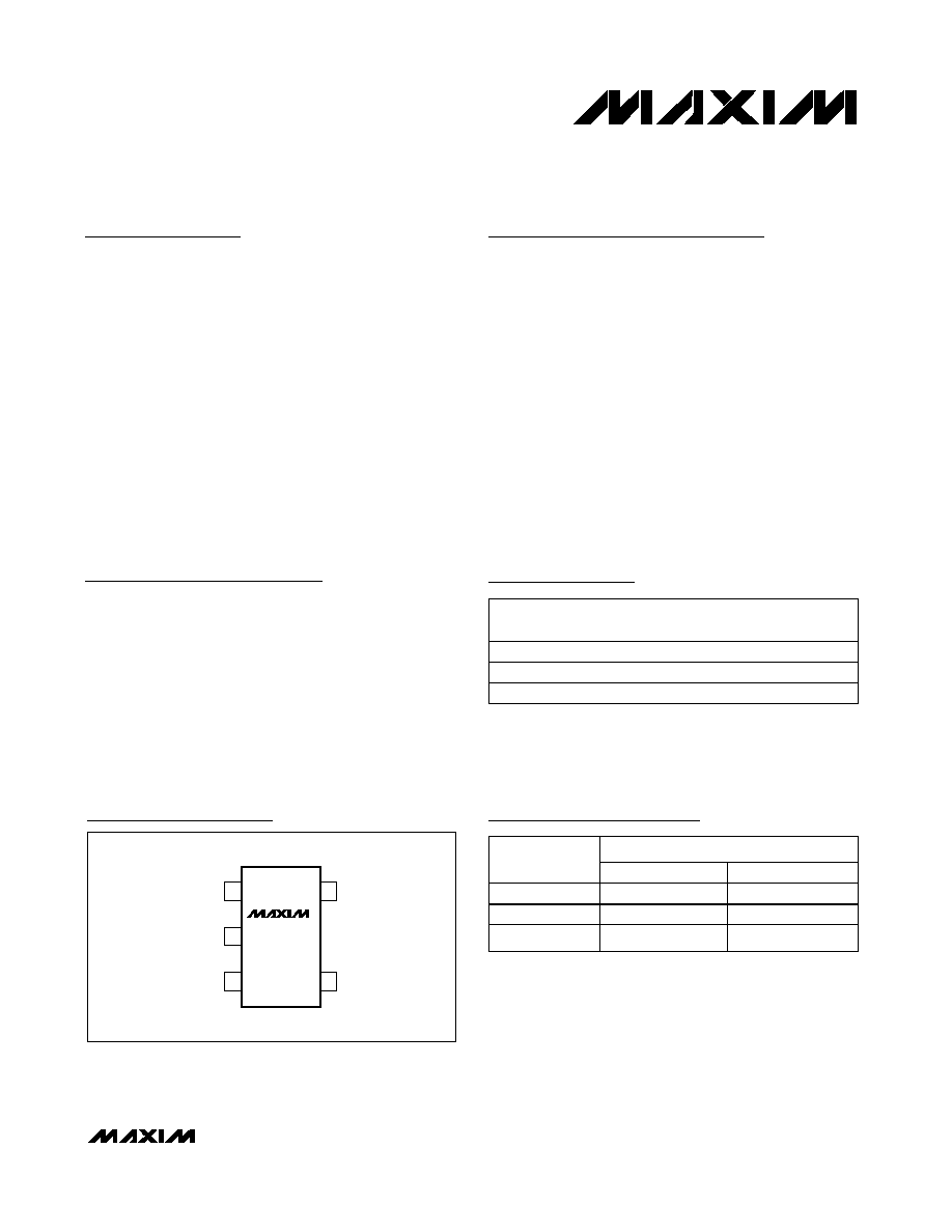
SOT23-5
TOP VIEW
2
3
4
Pin Configuration
Ordering Information
19-2141; Rev 0; 8/01
For pricing, delivery, and ordering information, please contact Maxim/Dallas Direct! at
1-888-629-4642, or visit Maxim's website at www.maxim-ic.com.
PA RT
TEMP.
RANGE
PIN-
PA CKA GE
TOP
MARK
MAX3406EUK
-40
°C to +85°C
5 SOT23-5
ADSV
MAX3407EUK
-40
°C to +85°C
5 SOT23-5
ADSW
MAX3408EUK
-40
°C to +85°C
5 SOT23-5
ADSX
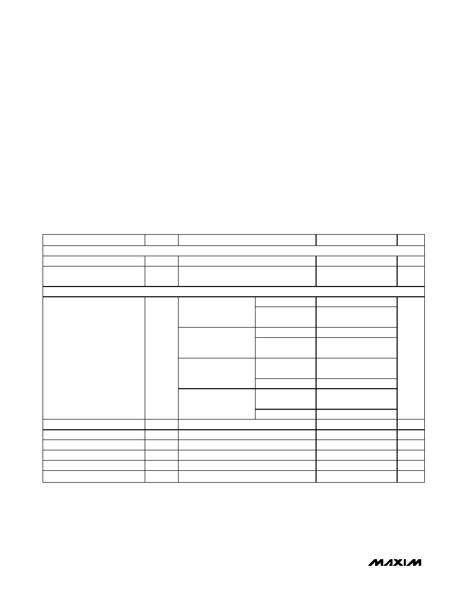
Selector Guide
TERMINATION
PA RT
ENABLE = 1
ENABLE = 0
MAX3406EUK
75
100
MAX3407EUK
75
120
MAX3408EUK
100
120
MAX3406/MAX3407/MAX3408
75
/100/120 Switchable Termination
Networks
2
_______________________________________________________________________________________
ABSOLUTE MAXIMUM RATINGS
ELECTRICAL CHARACTERISTICS
(V
CC
= +4.5V to +5.5V, T
A
=T
MIN
to T
MAX
, unless otherwise noted. Typical values are at V
CC
= +5V, T
A
= +25°C.) (Note 1)
Stresses beyond those listed under "Absolute Maximum Ratings" may cause permanent damage to the device. These are stress ratings only, and functional
operation of the device at these or any other conditions beyond those indicated in the operational sections of the specifications is not implied. Exposure to
absolute maximum rating conditions for extended periods may affect device reliability.
Note 1: All parameters tested at +25°C. Limits through temperature are guaranteed by design.
V
CC
...........................................................................-0.3V to +6V
ENABLE......................................................-0.3V to (V
CC
+ 0.3V)
A, B (applied individually) ...........................................-4V to +4V
Differential Voltage Across A-B ...................................-4V to +4V
Continuous Power Dissipation (T
A
= +70°C)
5-Pin SOT23 (derate 7.1mW/°C above +70°C)..........571mW
Operating Temperature Range ...........................-40°C to +85°C
Maximum Junction Temperature .....................................+150°C
Storage Temperature Range .............................-65°C to +150°C
Lead Temperature (soldering, 10s) .................................+300°C
PARAMETER
SYMBOL
CONDITIONS
MIN
TYP
MAX
UNITS
DC CHARACTERISTICS
Supply Range
V
CC
4.5
5.5
V
Supply Current
I
CC
V
CC
= +5.5V,
ENABLE = 0 or V
CC
30
50
µA
TERMINATOR NETWORK
MAX3406
97.5
100
102.5
-3.6V < V
AB
< ,+3.6V,
ENABLE = 0
MAX3407/
MAX3408
117
120
123
MAX3406
100
-3.6V < V
AB
< +3.6V,
ENABLE = 0,
frequency up to 36MHz
MAX3407/
MAX3408
120
MAX3406/
MAX3407
73.1
75
76.9
-3.6V < V
AB
< +3.6V,
ENABLE = 1
MAX3408
97.5
100
102.5
MAX3406/
MAX3407
75
On-Resistance
R
ON
-3.6V < V
AB
< +3.6V,
ENABLE = 1, frequency
up to 36MHz
MAX3408
100
Turn-On Time
t
ON
50
µs
Turn-Off Time
t
OFF
50
µs
Input Low Voltage
V
IL
0.8
V
Input High Voltage
V
IH
2.0
V
Input Current
I
IL
, I
IH
ENABLE = 0 or V
CC
-1
1
µA
Input Hysteresis
V
HYST
200
mV
(All voltages referenced to GND unless otherwise noted.)
MAX3406/MAX3407/MAX3408
75
/100/120 Switchable Termination
Networks
_______________________________________________________________________________________
3
60
70
90
80
100
110
-50
0
-25
25
50
75
100
RESISTANCE vs. TEMPERATURE
(MAX3406)
MAX3406/7/8 toc01
TEMPERATURE (
°C)
RESISTANCE (
)
ENABLE = 0
ENABLE = V
CC
60
80
70
100
90
110
130
120
-50
0
-25
25
50
75
100
RESISTANCE vs. TEMPERATURE
(MAX3407)
MAX3406/7/8 toc02
TEMPERATURE (
°C)
RESISTANCE (
)
ENABLE = 0
ENABLE = V
CC
90
95
105
100
115
110
120
130
125
-50
0
-25
25
50
75
100
RESISTANCE vs. TEMPERATURE
(MAX3408)
MAX3406/7/8 toc03
TEMPERATURE (
°C)
RESISTANCE (
)
ENABLE = 0
ENABLE = V
CC
60
80
70
100
90
110
120
-3.6
0
1.2
-2.4
-1.2
2.4
3.6
RESISTANCE vs. INPUT VOLTAGE
(MAX3406)
MAX3406/7/8 toc04
V
AB
(V)
RESISTANCE (
)
ENABLE = 0
ENABLE = V
CC
V
B
= 0
60
80
70
110
100
90
120
130
-3.6
0
1.2
-2.4
-1.2
2.4
3.6
RESISTANCE vs. INPUT VOLTAGE
(MAX3407)
MAX3406/7/8 toc05
V
AB
(V)
RESISTANCE (
)
ENABLE = 0
ENABLE = V
CC
V
B
= 0
90
105
100
95
115
110
125
120
130
-3.6
0
1.2
-2.4
-1.2
2.4
3.6
RESISTANCE vs. INPUT VOLTAGE
(MAX3408)
MAX3406/7/8 toc06
V
AB
(V)
RESISTANCE (
)
ENABLE = 0
ENABLE = V
CC
V
B
= 0
0
30
15
60
45
75
90
0.01
1
0.1
10
100
IMPEDANCE vs. FREQUENCY
75
MODE--MAX3406/MAX3407
MAX3406/7/8 toc07
FREQUENCY (MHz)
MAGNITUDE (
)
-90
-30
-60
30
0
60
90
PHASE (DEGREES)
MAGNITUDE
PHASE
0
40
20
80
60
100
120
0.01
1
0.1
10
100
IMPEDANCE vs. FREQUENCY
100
MODE--MAX3406/MAX3408
MAX3406/7/8 toc08
FREQUENCY (MHz)
MAGNITUDE (
)
-90
-30
-60
30
0
60
90
PHASE (DEGREES)
MAGNITUDE
PHASE
20
60
40
100
80
120
140
0.01
1
0.1
10
100
IMPEDANCE vs. FREQUENCY
120
MODE--MAX3407/MAX3408
MAX3406/7/8 toc09
FREQUENCY (MHz)
MAGNITUDE (
)
-90
-30
-60
30
0
60
90
PHASE (DEGREES)
MAGNITUDE
PHASE
Typical Operating Characteristics
(V
CC
= +5V, T
A
= +25°C, unless otherwise noted.)
Detailed Description
The MAX3406/MAX3407/MAX3408 are line-terminating
networks. They provide 75
, 100, and 120 termina-
tion to be compatible with twisted pair or coaxial cable.
The MAX3406/MAX3407/MAX3408 consume only 50µA
supply current and operate from a +4.5V to +5.5V
power supply. They are available in a space-saving 5-
pin SOT23 package. All specifications are guaranteed
over the extended temperature range of -40°C to
+85°C.
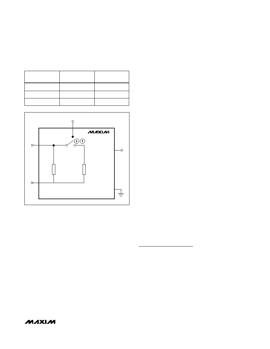
The ENABLE pin allows switching from one termination
value to another: 75
to 100 for the MAX3406, 75 to
120
for the MAX3407, and 100 to 120 for the
MAX3408 (Figure 1 and Table 1).
Applications Information
In order for the MAX3406/MAX3407/MAX3408 to termi-
nate transmission lines correctly, they should look like a
precision resistance. These devices look this way under
all operating conditions as can be seen from the Typical
Operating Characteristics. The very small variations in
resistance with temperature, input voltage, and frequen-
cy should not be of any concern in most applications,
though the users should be aware of them. The next
three sections describe these variations and explain
what end application effect they could have.
The function of a termination is to minimize line reflec-
tions by terminating a transmission line in its character-
istic impedance. The reflection coefficient for a line of
Z0 characteristic impedance terminated with a given
ZL is:
Voltage Reflection Coefficient = (ZL - Z0)/(ZL + Z0)
MAX3406/MAX3407/MAX3408
75
/100/120 Switchable Termination
Networks
4
_______________________________________________________________________________________
0%
20%
10%
50%
40%
30%
80%
70%
60%
90%
74.40
74.80
74.60
75.00
75.20
75.40
75.60
ACCURACY DISTRIBUTION
75
MODE
MAX3406/7/8 toc10
RESISTANCE (
)
PERCENTAGE OF PRODUCTION
0%
20%
10%
50%
40%
30%
80%
70%
60%
90%
98.8
99.6
99.2
100.0
100.4
100.8
101.2
ACCURACY DISTRIBUTION
100
MODE
MAX3406/7/8 toc11
RESISTANCE (
)
PERCENTAGE OF PRODUCTION
0%
20%
10%
50%
40%
30%
80%
70%
60%
90%
118.5
119.5
119.0
120.0
120.5
121.0
121.5
ACCURACY DISTRIBUTION
120
MODE
MAX3406/7/8 toc12
RESISTANCE (
)
PERCENTAGE OF PRODUCTION
Typical Operating Characteristics (continued)
(V
CC
= +5V, T
A
= +25°C, unless otherwise noted.)
Pin Description
PIN
NAME
FUNCTION
1
V
CC
Supply Voltage +4.5V to +5.5V. Bypass to GND with a 0.1
µF capacitor.
2
GND
Ground
3
ENABLE
Digital Control Input. Drive ENABLE high to turn on the internal switch, pull ENABLE low to disable
the internal switch.
4
B
Cable Terminator Terminal B
5
A
Cable Terminator Terminal A
This is the voltage that would be reflected from any line
termination. As ZL becomes equal to Z0, this quantity
becomes zero. Often this is expressed in dB and is
called return loss. Reflection coefficient values less
than 0.1 corresponding to a return loss of -20dB are
generally seen as adequate. The MAX3406/MAX3407/
MAX3408 will typically provide reflection coefficients
below 0.01 or -40dB return loss.
In most cases, Z0 and ZL are considered real resistive
quantities and the result is a dimensionless scalar
quantity, but the equation is valid in the complex case
as well.
Resistance vs. Temperature
The MAX3406/MAX3407/MAX3408 resistance is con-
stant over temperature. The typical temperature coeffi-
cient of resistance is 150ppm/°C. Over a -40°C to
+85°C range centered at +25°C, this would be a ±1%
change in resistance. The initial accuracy at room tem-
perature is ±1.5%. This provides improved perfor-
mance over discrete 5% resistors with a 100ppm temp-
co, which are typically used for termination, ±5.6%
worst case. The reflections from such a mistermination
are minimal and correspond to a worst-case reflection
coefficient for the MAX3406/MAX3407/MAX3408 of
±0.015 or a -36dB return loss.
Resistance vs. Input Voltage Range
The MAX3406/MAX3407/MAX3408 accept input volt-
ages (V
AB
) from -3.6V to +3.6V. There is virtually no
resistance variation over this range (0.02% typically).
The initial accuracy specifications in the data sheet
already account for resistance variations of the signal
voltage range.
Impedance vs. Frequency
As seen in the Typical Operating Characteristics, there
is a slight impedance variation in the MAX3406/
MAX3407/MAX3408 with frequency. The reactive com-
ponents are parasitic inductance and capacitance
associated with packaging, lead frame, and bond
wires. These impedance components are very small up
to frequencies above 20MHz. These parasitics are also
similar to those that would be present with a discrete
resistor terminator, and they can generally be ignored.
These effects should be evaluated for applications with
significant frequency content above 20MHz. This
applies to sine wave sources above 20MHz and square
and video sources above 8MHz. For all intended appli-
cations, E1/T1, Standard Video, etc. they can be
ignored.
Decoupling V
CC
The V
CC
pin for the MAX3406/MAX3407/MAX3408 must
be decoupled with a 0.1µF ceramic capacitor to GND
placed as close to the device as possible. This is
required for proper operation of the part.
Chip Information
TRANSISTOR COUNT: 102
PROCESS: BiCMOS
MAX3406/MAX3407/MAX3408
75
/100/120 Switchable Termination
Networks
_______________________________________________________________________________________
5
PART
R
AB
(
)
ENABLE = 1
R
AB
(
)
ENABLE = 0
MAX3406EUK
75
100
MAX3407EUK
75
120
MAX3408EUK
100
120
Table 1. Termination Mode Selection
GND
R2
R1
V
CC
MAX3406
MAX3407
MAX3408
ENABLE
B
A
Figure 1. Simplified Block Diagram