 | –≠–ª–µ–∫—Ç—Ä–æ–Ω–Ω—ã–π –∫–æ–º–ø–æ–Ω–µ–Ω—Ç: MAX3443E | –°–∫–∞—á–∞—Ç—å:  PDF PDF  ZIP ZIP |

Selector Guide
General Description
The MAX3440E≠MAX3444E fault-protected RS-485 and
J1708 transceivers feature
±60V protection from signal
faults on communication bus lines. Each device contains
one differential line driver with three-state output and one
differential line receiver with three-state input. The 1/4-unit-
load receiver input impedance allows up to 128 trans-
ceivers on a single bus. The devices operate from a 5V
supply at data rates of up to 10Mbps. True fail-safe inputs
guarantee a logic-high receiver output when the receiver
inputs are open, shorted, or connected to an idle data line.
Hot-swap circuitry eliminates false transitions on the
data bus during circuit initialization or connection to a
live backplane. Short-circuit current-limiting and ther-
mal shutdown circuitry protect the driver against exces-
sive power dissipation, and on-chip
±15kV ESD
protection eliminates costly external protection devices.
The MAX3440E≠MAX3444E are available in 8-pin SO
and PDIP packages and are specified over industrial
and automotive temperature ranges.
Applications
RS-422/RS-485 Communications
Truck and Trailer Applications
Industrial Networks
Telecommunications Systems
Automotive Applications
HVAC Controls
Features
o ±15kV ESD Protection
o ±60V Fault Protection
o Guaranteed 10Mbps Data Rate
(MAX3441E/MAX3443E)
o Hot Swappable for Telecom Applications
o True Fail-Safe Receiver Inputs
o Enhanced Slew-Rate-Limiting Facilitates
Error-Free Data Transmission
(MAX3440E/MAX3442E/MAX3444E)
o Allow Up to 128 Transceivers on the Bus
o -7V to +12V Common-Mode Input Range
o Automotive Temperature Range (-40∞C to +125∞C)
o Industry-Standard Pinout
MAX3440E≠MAX3444E
±15kV ESD-Protected, ±60V Fault-Protected,
10Mbps, Fail-Safe RS-485/J1708 Transceivers
________________________________________________________________ Maxim Integrated Products
1
TOP VIEW
1
2
3
4
8
5
V
CC
GND
DI
DE/RE
RO
FAULT
R
D
Rt
Rt
7
6
D
R
DE/RE
FAULT
DI
RO
A
B
1
2
3
4
8
7
6
5
V
CC
B
A
GND
DI
DE/RE
RO
FAULT
DIP/SO
DIP/SO
B
A
MAX3440E
MAX3441E
R
D
Pin Configurations and Typical Operating Circuits
Ordering Information
19-2666; Rev 0; 10/02
For pricing, delivery, and ordering information, please contact Maxim/Dallas Direct! at
1-888-629-4642, or visit Maxim's website at www.maxim-ic.com.
PART
TEMP RANGE
PIN-PACKAGE
MAX3440EESA
-40∞C to +85∞C
8 SO
MAX3440EEPA
-40∞C to +85∞C
8 PDIP
MAX3440EASA
-40∞C to +125∞C
8 SO
MAX3440EAPA
-40∞C to +125∞C
8 PDIP
PART
TYPE
DATA RATE
(Mbps)
LOW-POWER
SHUTDOWN
RECEIVER/DRIVER
ENABLE
TRANSCEIVERS
ON BUS
HOT
SWAP
MAX3440E
RS-485
0.25
No
Yes
128
Yes
MAX3441E
RS-485
2.5 to 10
No
Yes
128
Yes
MAX3442E
RS-485
0.25
Yes
Yes
128
Yes
MAX3443E
RS-485
2.5 to 10
Yes
Yes
128
Yes
MAX3444E
J1708
0.25
Yes
Yes
128
Yes (only RE)
Ordering Information continued at end of data sheet.
Pin Configurations and Typical Operating Circuits continued at end of data sheet.

MAX3440E≠MAX3444E
±15kV ESD-Protected, ±60V Fault-Protected,
10Mbps, Fail-Safe RS-485/J1708 Transceivers
2
_______________________________________________________________________________________
ABSOLUTE MAXIMUM RATINGS
Stresses beyond those listed under "Absolute Maximum Ratings" may cause permanent damage to the device. These are stress ratings only, and functional
operation of the device at these or any other conditions beyond those indicated in the operational sections of the specifications is not implied. Exposure to
absolute maximum rating conditions for extended periods may affect device reliability.
Voltages Referenced to GND
V
CC
........................................................................................+7V
FAULT, DE/RE, RE, DE, DE, DI, TXD..........-0.3V to (V
CC
+ 0.3V)
A, B (Note 1) ........................................................................±60V
RO ..............................................................-0.3V to (V
CC
+ 0.3V)
Short-Circuit Duration (RO, A, B) ...............................Continuous
Continuous Power Dissipation (T
A
= +70∞C)
8-Pin SO (derate 5.9mW/∞C above +70∞C)..................471mW
8-Pin PDIP (derate 9.09mW/∞C above +70∞C).............727mW
Operating Temperature Ranges
MAX344_EE_ _ ...............................................-40∞C to +85∞C
MAX344_EA_ _ .............................................-40∞C to +125∞C
Storage Temperature Range .............................-65∞C to +150∞C
Junction Temperature ......................................................+150∞C
Lead Temperature (soldering, 10s) .................................+300∞C
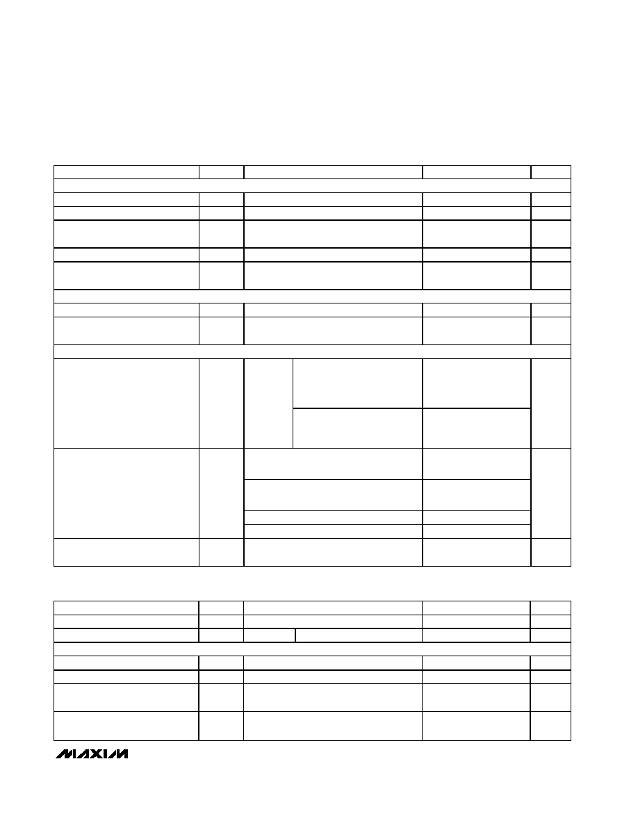
DC ELECTRICAL CHARACTERISTICS
(V
CC
= +4.75V to +5.25V, T
A
= T
MIN
to T
MAX
, unless otherwise noted. Typical values are at V
CC
= +5V and T
A
= +25∞C.)
PARAMETER
SYMBOL
CONDITIONS
MIN
TYP
MAX
UNITS
DRIVER
Figure 1, R
L
= 100
2
V
CC
Differential Driver Output
V
OD
Figure 1, R
L
= 54
1.5
V
CC
V
Change in Magnitude of
Differential Output Voltage
V
OD
Figure 1, R
L
= 100
or 54 (Note 2)
0.2
V
Driver Common-Mode
Output Voltage
V
OC
Figure 1, R
L
= 100
or 54
V
CC
/ 2
3
V
Change in Magnitude of
Common-Mode Voltage
V
OC
Figure 1, R
L
= 100
or 54 (Note 2)
0.2
V
DRIVER LOGIC
Driver Input High Voltage
V
DIH
2
V
Driver Input Low Voltage
V
DIL
0.8
V
Driver Input Current
I
DIN
±2
µA
0
V
OUT
+12V
+350
Driver Short-Circuit Output Current
(Note 3)
I
OSD
-7V
V
OUT
V
CC
-350
mA
(V
CC
- 1V)
V
OUT
+12V (Note 3)
+25
Driver Short-Circuit Foldback
Output Current
I
OSDF
-7V
V
OUT
+1V (Note 3)
-25
mA
RECEIVER
V
CC
= GND, V
A, B
= 12V
250
V
A, B
= -7V
-150
µA
Input Current
I
A,B
A, B
V
A, B
=
±60V
±6
mA
Receiver Differential Threshold
Voltage
V
TH
-7V
V
CM
+12V
-200
-50
mV
Receiver Input Hysteresis
V
TH
25
mV
Note 1: A, B must be terminated with 54
or 100 to guarantee ±60V fault protection.
MAX3440E≠MAX3444E
±15kV ESD-Protected, ±60V Fault-Protected,
10Mbps, Fail-Safe RS-485/J1708 Transceivers
_______________________________________________________________________________________
3
PARAMETER
SYMBOL
CONDITIONS
MIN
TYP
MAX
UNITS
RECEIVER LOGIC
Output High Voltage
V
OH
Figure 2, I
OH
= -1.6mA
V
CC
- 0.6
V
Output Low Voltage
V
OL
Figure 2, I
OL
= 1mA
0.4
V
Three-State Output Current at
Receiver
I
OZR
0
V
A, B
V
CC
±1
µA
Receiver Input Resistance
R
IN
-7V
V
CM
+12V
48
k
Receiver Output Short-Circuit
Current
I
OSR
0
V
RO
V
CC
±95
mA
CONTROL
Control Input High Voltage
V
CIH
DE, DE, RE, DE/RE
2
V
Input Current Latch During First
Rising Edge
I
IN
DE, DE/RE, RE
90
µA
SUPPLY CURRENT
MAX3440E (DE/RE = V
CC
),
MAX3442E (DE = V
CC
,
RE = GND),
MAX3444E (DE = RE = GND)
30
Normal Operation
I
Q
No load,
DI = V
CC
or GND
MAX3441E (DE/RE = V
CC
),
MAX3443E (DE = V
CC
,
RE = GND)
10
mA
DE = GND, RE = V
CC
(MAX3442E/
MAX3443E)
20
DE = GND, RE = V
CC
, T
A
= +25∞C
(MAX3442E/MAX3443E)
10
DE = RE = V
CC
(MAX3444E)
100
Supply Current in Shutdown Mode
I
SHDN
DE = RE = V
CC
, T
A
= +25∞C (MAX3444E)
10
µA
Supply Current with Output
Shorted to
±60V
I
SHRT
DE = GND, RE = GND, no load
output in three-state (MAX3443E)
±15
mA
DC ELECTRICAL CHARACTERISTICS (continued)
(V
CC
= +4.75V to +5.25V, T
A
= T
MIN
to T
MAX
, unless otherwise noted. Typical values are at V
CC
= +5V and T
A
= +25∞C.)
PARAMETER
SYMBOL
CONDITIONS
MIN
TYP
MAX
UNITS
Overvoltage Protection
A, B; R
SOURCE
= 0, R
L
= 54
±60
V
ESD Protection
A, B
Human Body Model
±15
kV
FAULT DETECTION
Receiver Differential Threshold
F
DIPH
V
CM
= 0, high limit
270
450
mV
Receiver Differential Threshold
F
DIPL
V
CM
= 0, low limit
-450
-270
mV
Fault-Detection Common-Mode
Input Voltage Positive
12
V
Fault-Detection Common-Mode
Input Voltage Negative
-7
V
PROTECTION SPECIFICATIONS
(V
CC
= +4.75V to +5.25V, T
A
= T
MIN
to T
MAX
, unless otherwise noted. Typical values are at V
CC
= +5V and T
A
= +25∞C.)

MAX3440E≠MAX3444E
±15kV ESD-Protected, ±60V Fault-Protected,
10Mbps, Fail-Safe RS-485/J1708 Transceivers
4
_______________________________________________________________________________________
PARAMETER
SYMBOL
CONDITIONS
MIN
TYP
MAX
UNITS
MAX3440E/MAX3442E,
Figure 3, R
L
= 54
, C
L
= 50pF
Driver Propagation Delay
t
PLHA,
t
PLHB
MAX3444E, R
DIFF
= 60
, C
DIFF
= 100pF
2000
ns
Driver Differential Propagation Delay
t
DPLH
,
t
DPHL
Figure 4, R
L
= 54
, C
L
= 50pF
2000
ns
Driver Differential Output
Transition Time
t
LH
,t
HL
Figure 4, R
L
= 54
, C
L
= 50pF
200
2000
ns
Driver Output Skew
t
S KEWAB
,
t
S KEWBA
R
L
= 54
, C
L
= 50pF,
t
SKEWAB
= |t
PLHA
- t
PHLB
|,
t
SKEWBA
= |t
PLHB
- t
PHLA
|
350
ns
Differential Driver Output Skew
t
DSKEW
R
L
= 54
, C
L
= 50pF,
t
DSKEW
= |t
DPLH
- t
DPHL
|
200
ns
Maximum Data Rate
f
MAX
250
kbps
Driver Enable Time to Output High
t
PDZH
Figure 5, R
L
= 500
, C
L
= 50pF
2000
ns
Driver Disable Time from Output High
t
PDHZ
Figure 5, RL = 500
, C
L
= 50pF
2000
ns
Driver Enable Time from Shutdown to
Output High
t
PDHS
Figure 5, RL = 500
, C
L
= 50pF
(MAX3442E/MAX3444E)
4.2
µs
Driver Enable Time to Output Low
t
PDZL
Figure 6, R
L
= 500
, C
L
= 50pF
2000
ns
Driver Disable Time from Output Low
t
PDLZ
Figure 6, R
L
= 500
, C
L
= 50pF
2000
ns
Driver Enable Time from Shutdown to
Output Low
t
PDLS
Figure 6, R
L
= 500
, C
L
= 50pF
(MAX3442E/MAX3444E)
4.2
µs
Driver Time to Shutdown
t
SHDN
R
L
= 500
, C
L
= 50p F ( M AX 3442E /M AX 3444E ) 800
ns
Receiver Propagation Delay
t
RPLH
,
t
RPHL
Figure 7, C
L
= 20pF, V
ID
= 2V, V
CM
= 0
2000
ns
Receiver Output Skew
t
RSKEW
C
L
= 20pF, t
RSKEW
= |t
RPLH
- t
RPHL
|
200
ns
Receiver Enable Time to Output High
t
RPZH
Figure 8, R
L
= 1k
, C
L
= 20pF
2000
ns
Recei ver D i sab l e Ti m e fr om Outp ut H i g h
t
RPHZ
Figure 8, R
L
= 1k
, C
L
= 20pF
2000
ns
Receiver Wake Time from Shutdown
t
RPWAKE
Figure 8, R
L
= 1k
, C
L
= 20pF
(MAX3442E/MAX3444E)
4.2
µs
Receiver Enable Time to Output Low
t
RPZL
Figure 8, R
L
= 1k
, C
L
= 20pF
2000
ns
Recei ver D i sab l e Ti m e fr om Outp ut Low
t
RPLZ
Figure 8, R
L
= 1k
, C
L
= 20pF
2000
ns
Receiver Time to Shutdown
t
SHDN
R
L
= 500
, C
L
= 50pF
(MAX3442E/MAX3444E)
800
ns
SWITCHING CHARACTERISTICS (MAX3440E/MAX3442E/MAX3444E)
(V
CC
= +4.75V to +5.25V, T
A
= T
MIN
to T
MAX
, unless otherwise noted. Typical values are at V
CC
= +5V and T
A
= +25∞C.)

MAX3440E≠MAX3444E
±15kV ESD-Protected, ±60V Fault-Protected,
10Mbps, Fail-Safe RS-485/J1708 Transceivers
_______________________________________________________________________________________
5
PARAMETER
SYMBOL
CONDITIONS
MIN
TYP
MAX
UNITS
Driver Propagation Delay
t
PLHA,
t
PLHB
Figure 3, R
L
= 27
, C
L
= 50pF
60
ns
Driver Differential Propagation Delay
t
DPLH
,
t
DPHL
Figure 4, R
L
= 54
, C
L
= 50pF
60
ns
Driver Differential Output
Transition Time
t
LH
,t
HL
Figure 4, R
L
= 54
, C
L
= 50pF
25
ns
Driver Output Skew
t
SKEWAB
,
t
SKEWBA
R
L
= 54
, C
L
= 50pF,
t
SKEWAB
= |t
PLHA
- t
PHLB
|,
t
SKEWBA
= |t
PLHB
- t
PHLA
|
10
ns
Differential Driver Output Skew
t
DSKEW
R
L
= 54
, C
L
= 50pF,
t
DSKEW
= |t
DPLH
- t
DPHL
|
10
ns
Maximum Data Rate
f
MAX
10
Mbps
Driver Enable Time to Output High
t
PDZH
Figure 5, R
L
= 500
, C
L
= 50pF
1200
ns
Driver Disable Time from Output High
t
PDHZ
Figure 5, R
L
= 500
, C
L
= 50pF
1200
ns
Driver Enable Time from Shutdown to
Output High
t
PDHS
Figure 5, R
L
= 500
, C
L
= 50pF (MAX3443E)
4.2
µs
Driver Enable Time to Output Low
t
PDZL
Figure 6, R
L
= 500
, C
L
= 50pF
1200
ns
Driver Disable Time from Output Low
t
PDLZ
Figure 6, R
L
= 500
, C
L
= 50pF
1200
ns
Driver Enable Time from Shutdown to
Output Low
t
PDLS
Figure 6, R
L
= 500
, C
L
= 50pF (MAX3443E)
4.2
µs
Driver Time to Shutdown
t
SHDN
Fi g ur e 6, R
L
= 500
, C
L
= 50p F ( M AX 3443E ) 800
ns
Receiver Propagation Delay
t
RPLH
,
t
RPHL
Figure 7, C
L
= 20pF, V
ID
= 2V, V
CM
= 0
85
ns
Receiver Output Skew
t
RSKEW
C
L
= 20pF, t
RSKEW
= |t
RPLH
- t
RPHL
|
15
ns
Receiver Enable Time to Output High
t
RPZH
Figure 8, R
L
= 1k
, C
L
= 20pF
400
ns
Recei ver D i sab l e Ti m e fr om Outp ut H i g h
t
RPHZ
Figure 8, R
L
= 1k
, C
L
= 20pF
400
ns
Receiver Wake Time from Shutdown
t
RPWAKE
Figure 8, R
L
= 1k
, C
L
= 20pF (MAX3443E)
4.2
µs
Receiver Enable Wake Time from
Shutdown
t
RPSH
Figure 8, R
L
= 1k
, C
L
= 20pF
400
ns
Recei ver D i sab l e Ti m e fr om Outp ut Low
t
RPLZ
Figure 8, R
L
= 1k
, C
L
= 20pF
400
ns
Receiver Time to Shutdown
t
SHDN
R
L
= 500
, C
L
= 50pF (MAX3443E)
800
ns
SWITCHING CHARACTERISTICS (MAX3441E/MAX3443E)
(V
CC
= +4.75V to +5.25V, T
A
= T
MIN
to T
MAX
, unless otherwise noted. Typical values are at V
CC
= +5V and T
A
= +25∞C.)
Note 2:
V
OD
and
V
OC
are the changes in V
OD
and V
OC
, respectively, when the DI input changes state.
Note 3: The short-circuit output current applies to peak current just before foldback current limiting; the short-circuit foldback output
current applies during current limiting to allow a recovery from bus contention.