 | –≠–Ľ–Ķ–ļ—ā—Ä–ĺ–Ĺ–Ĺ—č–Ļ –ļ–ĺ–ľ–Ņ–ĺ–Ĺ–Ķ–Ĺ—ā: MAX3793 | –°–ļ–į—á–į—ā—Ć:  PDF PDF  ZIP ZIP |

General Description
The MAX3793 transimpedance amplifier provides a
compact low-power solution for applications from
1Gbps up to 4.25Gbps.
The MAX3793 features 195nA input-referred noise,
3.5k transimpedance gain, 2.9GHz bandwidth (C
IN
=
0.3pF) and 2.8mA
P-P
input overload. Operating from a
+3.3V supply, the MAX3793 consumes only 106mW. An
integrated filter resistor provides positive bias for the
photodiode. These features, combined with a small die
size, allow easy assembly into a TO-46 header with a
photodiode. The MAX3793 also includes an average
photocurrent monitor.
The MAX3793 has a typical optical sensitivity of -20dBm
(0.55A/W) at 4.25Gbps. Typical optical overload is
at 4dBm. The MAX3793 and the MAX3794 limiting
amplifiers provide a complete solution for multirate
receiver applications.
Applications
SFF/SFP Transceiver Modules from 1Gbps to
4.25Gbps
Gigabit Ethernet Optical Receivers
Multirate Fibre-Channel Optical Receivers
Features
4.7ps
P-P
Deterministic Jitter (DJ)
195nA
RMS
Input-Referred Noise
2.9GHz Small-Signal Bandwidth
2.8mA
P-P
AC Overload
Photocurrent Output Monitor
3.5k Differential Gain
Compact Die Size (30 mils x 50 mils)
MAX3793
1Gbps to 4.25Gbps Multirate Transimpedance
Amplifier with Photocurrent Monitor
________________________________________________________________ Maxim Integrated Products
1
Ordering Information
19-3467; Rev 0; 10/04
For pricing, delivery, and ordering information, please contact Maxim/Dallas Direct! at
1-888-629-4642, or visit Maxim's website at www.maxim-ic.com.
PART
TEMP RANGE
PIN-PACKAGE
MAX3793E/D
-40įC to +85įC
Dice*
DS1856/
DS1859
MAX3793
MAX3794*
FILT
OUT+
OUT-
IN
V
CC
GND
LOS
DISABLE
IN+
IN-
OUT+
OUT-
V
CC
HOST
BOARD
SFP OPTICAL RECEIVER
MOD-DEF1
MOD-DEF2
V
CC
C
FILT
C
VCC
MON
R
MON
BWSEL
RATE_SELECT
0.1ĶF
0.1ĶF
0.1ĶF
0.1ĶF
4.7k
TO
10k
*FUTURE PRODUCT
Typical Application Circuit
*Dice are designed to operate from -40įC to +85įC ambient
temperature, but are tested and guaranteed only at T
A
= +25įC.

MAX3793
1Gbps to 4.25Gbps Multirate Transimpedance
Amplifier with Photocurrent Monitor
2
_______________________________________________________________________________________
ABSOLUTE MAXIMUM RATINGS
ELECTRICAL CHARACTERISTICS
(V
CC
= +2.97V to +3.63V, T
A
= -40įC to +85įC. Typical values are at V
CC
= +3.3V, source capacitance C
IN
= 0.60pF, T
A
= +25įC,
unless otherwise noted.) (Notes 1, 2)
Stresses beyond those listed under "Absolute Maximum Ratings" may cause permanent damage to the device. These are stress ratings only, and functional
operation of the device at these or any other conditions beyond those indicated in the operational sections of the specifications is not implied. Exposure to
absolute maximum rating conditions for extended periods may affect device reliability.
Power-Supply Voltage (V
CC
) .................................-0.5V to +4.5V
Continuous CML Output Current
(OUT+, OUT-) ...............................................-25mA to +25mA
Continuous Input Current (IN)...............................-4mA to +4mA
Continuous Input Current (FILTER).......................-8mA to +8mA
Operating Junction Temperature Range (T
J
) ....-55įC to +150įC
Storage Ambient Temperature Range (T
STG
) ...-55įC to +150įC
Die Attach Temperature...................................................+400įC
PARAMETER
SYMBOL
CONDITIONS
MIN
TYP
MAX
UNITS
Power-Supply Current
I
CC
Measured with AC-coupled output
32
46
mA
Input Bias Voltage
1.0
V
Input Overload
I
OL
(Note 3)
2.2
2.8
mA
P-P
BER = 10
-12
, K28.5, at 1.0625Gbps
-23.5
BER = 10
-12
, K28.5, at 2.125Gbps
-23
Optical Input Sensitivity
(850nm, r
e
= 10dB,
Responsiveness = 0.55A/W)
BER = 10
-12
, K28.5, at 4.25Gbps
-20
dBm
BW = 933MHz, 4th-order Bessel filter
195
264
BW = 2000MHz, 4th-order Bessel filter
377
420
Input-Referred Noise (Notes 3, 4)
Unfiltered output
449
615
nA
RMS
Differential Transimpedance
I
IN
= 20ĶA
AVE
2.8
3.5
4.5
k
-3dB, C
IN
= 0.6pF (Note 3)
1.9
2.5
3.2
Small-Signal Bandwidth
BW
-3dB, C
IN
= 0.3pF (Note 5)
2.36
2.9
3.56
GHz
Gain Peaking
(Note 3)
0
dB
Low-Frequency Cut-Off
-3dB, I
IN
= 20ĶA
AVE
(Note 3)
70
kHz
I
IN
= 20ĶA
P-P
,
K28.5, at 4.25Gbps
4.7
11
20ĶA
P-P
< I
IN
< 100ĶA
P-P
,
K28.5, at
4.25Gbps
6
16
10
27
100ĶA
P-P
< I
IN
< 2.2mA
P-P
,
K28.5, at 4.25Gbps
T
A
= +100įC
10
Deterministic Jitter
(Notes 3, 6)
DJ
T
A
= +100įC, 100ĶA
P-P
< I
IN
< 2.2mA
P-P
,
K28.5, at 4.25Gbps
10
ps
P-P
Photodiode Resistor
R
FILT
600
750
930
Differential Output Resistance
R
OUT
85
100
115
Maximum Differential Output
Voltage
V
OD(MAX)
Outputs terminated by 50 to V
CC
, I
IN
>
100ĶA
P-P
220
480
mV
P-P
73
95
Output Edge Transition Time
Outputs terminated by 50
to V
CC
20% to 80%, I
IN
>
200ĶA
P-P
(Note 3)
T
A
= +100įC
90
ps

MAX3793
1Gbps to 4.25Gbps Multirate Transimpedance
Amplifier with Photocurrent Monitor
_______________________________________________________________________________________
3
Note 1: Die parameters are production tested at room temperature only, but are guaranteed by design and characterization from
-40įC to +85įC.
Note 2: Source capacitance represents the total external capacitance at the IN pad during characterization of the noise and band-
width parameters.
Note 3: Guaranteed by design and characterization.
Note 4: Input-referred noise is:
Note 5: Values are derived by calculation from the C
IN
= 0.6pF measurements.
Note 6: DJ is the sum of pulse-width distortion (PWD) and pattern-dependent jitter (PDJ). DJ is measured using a 3.2GHz 4th-order
Bessel filter on the input.
Note 7: Power-supply noise rejection PSNR = -20log(V
OUT
/ V
CC
), where V
OUT
is the change in differential output voltage and
V
CC
is the noise on V
CC
.
Note 8: Gain stability is defined as
(A
MON
- A
MON-NOM
) / (A
MON-NOM
)
over the listed current range, temperature, and supply variation. Nominal gain is measured at V
CC
= +3.3V and +25įC.
RMS Output Noise
Gain at f
MHz
=
100
ELECTRICAL CHARACTERISTICS (continued)
(V
CC
= +2.97V to +3.63V, T
A
= -40įC to +85įC. Typical values are at V
CC
= +3.3V, source capacitance C
IN
= 0.60pF, T
A
= +25įC,
unless otherwise noted.) (Notes 1, 2)
PARAMETER
SYMBOL
CONDITIONS
MIN
TYP
MAX
UNITS
Frequency 1GHz
18
Differential Output Return Loss
1GHz < frequency 4GHz
9
dB
Frequency 1GHz
14
Single-Ended Output Return Loss
1GHz < frequency 4GHz
11
dB
I
IN
= 0, f < 1MHz
47
Power-Supply Noise Rejection
(Note 7)
PSNR
I
IN
= 0, 1MHz f < 10MHz
22
dB
Minimum Photocurrent to be
Detected
I
AVGMIN
2
ĶA
Maximum Photocurrent to be
Detected
I
AVGMAX
1
mA
Maximum Photocurrent Monitor
Output Offset
I
MON
(OFFSET)
I
IN
= 0ĶA
P-P
10
ĶA
Photocurrent Monitor Output
Offset Temperature Dependency
I
MON
(OFFSET)
I
IN
= 0ĶA
P-P
I
MON(OFFSET)
= ABS (I
MON(OFFSET)
(-40įC) - I
MON(OFFSET)
(+100įC))
0.21
ĶA
Monitor Output Compliance
Voltage
V
MON
0
2
V
Photocurrent Monitor Gain
A
MON
2ĶA I
AVG
1.0mA
1
A/A
Photocurrent Monitor Gain
Stability
2ĶA I
AVG
1.0mA (Notes 3, 8)
-10
+10
%
Photocurrent Monitor Gain
Bandwidth
2ĶA I
AVG
1.0mA
7
MHz
MAX3793
1Gbps to 4.25Gbps Multirate Transimpedance
Amplifier with Photocurrent Monitor
4
_______________________________________________________________________________________
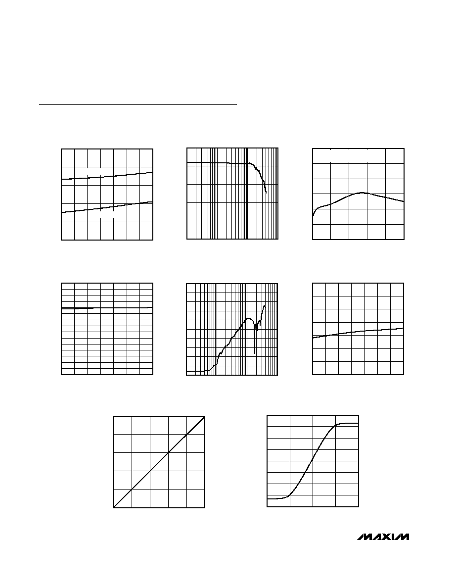
Typical Operating Characteristics
(V
CC
= +3.3V, C
IN
= 0.6pF, T
A
= +25įC, unless otherwise noted.)
INPUT-REFERRED NOISE
vs. TEMPERATURE
MAX3793 toc01
TEMPERATURE (įC)
INPUT-REFERRED NOISE (nA
RMS
)
80
60
40
20
0
-20
200
300
400
500
600
100
-40
100
UNFILTERED
BW = 2.0GHz
FREQUENCY RESPONSE
MAX3793 toc02
FREQUENCY (Hz)
GAIN (dB
)
1G
100M
55
60
65
70
75
50
10M
10G
DETERMINISTIC JITTER
vs. INPUT AMPLITUDE
MAx3793 toc03
INPUT AMPLITUDE (A
P-P
)
DETERMINISTIC JITTER (ps
P-P
)
1.6m
1.2m
800Ķ
400Ķ
3
6
9
12
15
18
0
20Ķ
2.0m
DATA RATE = 4.25Gbps
K28.5 PATTERN, UNFILTERED INPUT
SMALL-SIGNAL TRANSIMPEDANCE
vs. TEMPERATURE
MAX3793 toc04
TEMPERATURE (įC)
TRANSIMPEDANCE (dB
)
80
60
40
20
0
-20
65
70
75
60
-40
100
DIFFERENTIAL S
22
vs. FREQUENCY
MAX3793 toc05
FREQUENCY (Hz)
S
22
(dB)
1G
100M
-45
-40
-35
-30
-25
-20
-15
-10
-5
0
-50
10M
10G
SUPPLY CURRENT
vs. TEMPERATURE
MAX3793 toc06
TEMPERATURE (įC)
SUPPLY CURRENT (mA)
80
60
40
20
0
-20
10
20
30
40
50
60
70
0
-40
100
MONITOR OUTPUT CURRENT
vs. AVERAGE INPUT CURRENT
MAX3793 toc07
AVERAGE INPUT CURRENT (mA)
MONITOR OUTPUT CURRENT (mA)
0.8
0.6
0.4
0.2
0.2
0.4
0.6
0.8
1.0
0
0
1.0
DC TRANSFER FUNCTION
(V
FILT
= 0V)
MAX3793 toc08
INPUT CURRENT (ĶA)
OUTPUT VOLTAGE (mV)
50
0
-50
-150
-100
-50
0
50
100
150
200
-200
-100
100

MAX3793
1Gbps to 4.25Gbps Multirate Transimpedance
Amplifier with Photocurrent Monitor
_______________________________________________________________________________________
5
Typical Operating Characteristics (continued)
(V
CC
= +3.3V, C
IN
= 0.6pF, T
A
= +25įC, unless otherwise noted.)
EYE DIAGRAM
INPUT = 20ĶA
P-P
, DATA RATE = 1.0625Gbps
MAX3793 toc09
200ps/div
10mV/div
K28.5 PATTERN
EYE DIAGRAM
INPUT = 20ĶA
P-P
, DATA RATE = 2.125Gbps
MAX3793 toc10
100ps/div
10mV/div
K28.5 PATTERN
EYE DIAGRAM
INPUT = 20ĶA
P-P
, DATA RATE = 4.25Gbps
MAX3793 toc11
48ps/div
10mV/div
K28.5 PATTERN
EYE DIAGRAM
INPUT = 2.2mA
P-P
, DATA RATE = 4.25Gbps
MAX3793 toc12
48ps/div
40mV/div
K28.5 PATTERN
EYE DIAGRAM T
A
= +100įC
INPUT = 20ĶA
P-P
, DATA RATE = 4.25Gbps
MAX3793 toc13
48ps/div
10mV/div
K28.5 PATTERN
MAX3793 toc14
I
MON
CHANGE OVER TEMPERATURE (ĶA)
% OF UNITS
0.56-0.7
0.42-0.56
0.28-0.42
0.14-0.28
5
10
15
20
25
30
35
40
45
0
0-0.14
0.7-0.84
PHOTOCURRENT MONITOR OFFSET
TEMPERATURE DEPENDENCY HISTOGRAM