 | ÐлекÑÑоннÑй компоненÑ: MAX3832 | СкаÑаÑÑ:  PDF PDF  ZIP ZIP |
Äîêóìåíòàöèÿ è îïèñàíèÿ www.docs.chipfind.ru
For free samples & the latest literature: http://www.maxim-ic.com, or phone 1-800-998-8800.
For small orders, phone 1-800-835-8769.
General Description
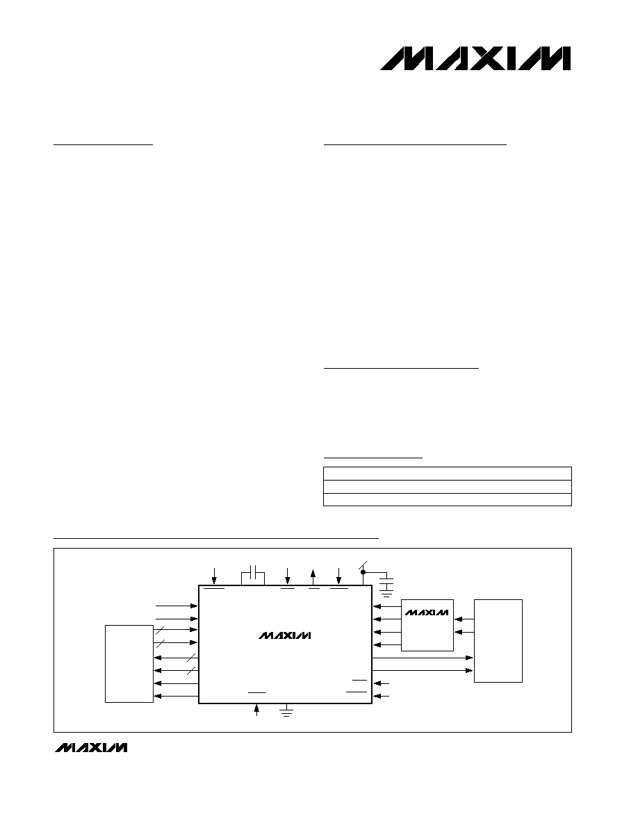
The MAX3831/MAX3832 are 4:1 multiplexers (muxes)
and 1:4 demultiplexers (demuxes) with automatic chan-
nel assignment. Operating from a single +3.3V supply,
the mux receives four parallel, 622Mbps SDH/SONET
channels. These channels are bit interleaved to gener-
ate a serial data stream of 2.488Gbps for interfacing to
an optical or an electrical driver. A 10-bit-wide elastic
buffer tolerates up to ±7.5ns skew between any parallel
data input and the reference clock. An external
155MHz reference clock is required for the on-chip PLL
to synthesize a high-frequency 2.488GHz clock for tim-
ing the outgoing data streams.
The MAX3831/MAX3832's demux receives 2.488Gbps
serial data and the 2.488GHz clock from an external
clock/data recovery device (MAX3876), converting it to
four 622Mbps LVDS outputs. The MAX3831 provides a
622MHz LVDS clock output, and the MAX3832 pro-
vides a 155MHz LVDS clock output. An internal frame
detector looks for a 622Mbps SDH/SONET framing pat-
tern and rolls the demux to maintain proper channel
assignment at the outputs.
These devices also include an embedded pattern gen-
erator that enables a full-speed, built-in self-test (BIST).
Two different loopback modes provide system test flexi-
bility. A TTL loss-of-frame monitor is included. The
MAX3831/MAX3832 are available in 64-pin TQFP-EP
(exposed paddle) packages and are specified over the
upper commercial (0°C to +85°C) temperature range.
Features
o +3.3V Single Supply
o 1.45W Power Dissipation (MAX3831)
o 4-Channel Mux/Demux with Fully Integrated
2.488GHz Clock Generator
o Frame Detection Maintains Channel Assignment
o ±7.5ns Elastic Store Range
o 2.5ps RMS Serial-Data Output Random Jitter
o 8ps Serial-Data Output Deterministic Jitter
o 622Mbps LVDS Parallel Input/Output
o 2.488Gbps Serial CML Input/Output
o On-Chip Pattern Generator Provides
High-Speed BIST
o System Test Flexibility: System Loopback,
Line Loopback
o Loss-of-Frame Indicator
Applications
SDH/SONET Backplanes
ATM Switching Networks
High-Speed Parallel Links
Line Extenders
Intrarack/Subrack
Dense Digital Cross-
Interconnects
Connects
MAX3831/MAX3832
+3.3V, 2.5Gbps, SDH/SONET, 4-Channel
Interconnect Mux/Demux ICs with Clock Generator
________________________________________________________________ Maxim Integrated Products
1
19-1534; Rev 1; 10/99
TTL
LVDS
LVDS
LVDS
4
4
4
4
TTL
TTL
TTL
TTL
2.5Gbps
CDR
CMOS
OVERHEAD
2.5Gbps
OPTICAL
TRANSCEIVER
TTL
CML
CML
GND
TRIEN
+3.3V
0.33
µF
0.1
µF
V
CC
FIL+
FIL-
PDI1+ TO PDI4+
PDI1- TO PDI4-
PDO1+ TO PDO4+
PDO1- TO PDO4-
PCLKO+
PCLKO-
SCLKI-
SCLKI+
SDI-
SDI+
SDO+
SDO-
MAX3831
MAX3832
MAX3876
LVDS
RCLKI+
RCLKI-
RSETES
LBEN
RSETFR
TEST
LOF
PLBEN
155MHz REF
CLOCK INPUT
TTL
Typical Application Circuit
Ordering Information
PART
MAX3831UCB
MAX3832UCB
0°C to +85°C
0°C to +85°C
TEMP. RANGE
PIN-PACKAGE
64 TQFP-EP
64 TQFP-EP
Pin Configuration appears at end of data sheet.
MAX3831/MAX3832
+3.3V, 2.5Gbps, SDH/SONET, 4-Channel
Interconnect Mux/Demux ICs with Clock Generator
2
_______________________________________________________________________________________
ABSOLUTE MAXIMUM RATINGS
DC ELECTRICAL CHARACTERISTICS
(V
CC
= +3.0V to +3.6V, LVDS differential load = 100
±1%, CML load = 50 ±1% to V
CC
, all TTL inputs are open, T
A
= 0°C to
+85°C, unless otherwise noted. Typical values are at T
A
= +25°C and V
CC
= +3.3V.)
Stresses beyond those listed under "Absolute Maximum Ratings" may cause permanent damage to the device. These are stress ratings only, and functional
operation of the device at these or any other conditions beyond those indicated in the operational sections of the specifications is not implied. Exposure to
absolute maximum rating conditions for extended periods may affect device reliability.
Positive Supply Voltage (V
CC
)...............................-0.5V to +5.0V
Input Voltage (LVDS, TTL)..........................-0.5V to (V
CC
+ 0.5V)
CML Input Voltage ..........................(V
CC
- 0.8V) to (V
CC
+ 0.5V)
FIL+, FIL- Voltage.......................................-0.5V to (V
CC
+ 0.5V)
TTL Output Voltage ....................................-0.5V to (V
CC
+ 0.5V)
LVDS Output Voltage ..................................-0.5V to (V
CC
+0.5V)
CML Output Currents..........................................................22mA
Continuous Power Dissipation (T
A
= +85°C) (Note 1)
64-Pin TQFP-EP (derate 40.0mW/°C above +85°C) .........2.6W
Operating Temperature Range...............................0°C to +85°C
Storage Temperature Range .............................-60°C to +150°C
Lead Temperature (soldering, 10sec) .............................+300°C
Short outputs together (Note 3)
TRIEN = V
CC
TRIEN = GND
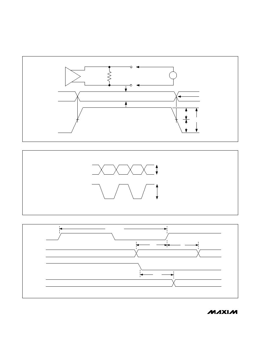
Figure 1
LVDS input, V
OS
= 1.2V
CONDITIONS
V
V
CC
- V
CC
+
0.6
0.4
V
IS
Single-Ended Input Voltage Range
V
V
CC
- 0.2
Output Common-Mode Voltage
85
100
115
Differential Output Impedance
mVp-p
640
800
1000
V
ODp-p
Differential Output Voltage
mA
12
Output Current
80
120
Differential Output Impedance
M
>1
mV
±25
V
OS
Change in Magnitude of Output
Offset Voltage for Complementary
States
V
1.125
1.275
V
OS
Output Offset Voltage
mV
±25
V
OD
Change in Magnitude of
Differential Output Voltage for
Complementary States
mA
440
580
I
CC
Supply Current
mV
250
400
V
OD
Differential Output Voltage
V
0.925
V
OL
Output Voltage Low
V
1.475
V
OH
Output Voltage High
µA
270
I
OS
Input Common-Mode Current
mV
0
2400
V
IN
Input Voltage Range
mV
-100
+100
V
IDTH
Differential Input Threshold
mV
90
V
HYST
Threshold Hysteresis
85
100
115
R
IN
Input Impedance
UNITS
MIN
TYP
MAX
SYMBOL
PARAMETER
Figure 2
85
100
115
Differential Input Impedance
mVp-p
400
1200
Differential Input Voltage Swing
LVDS INPUTS AND OUTPUTS
CML INPUTS AND OUTPUTS
Note 1: Based on empirical data from the MAX3831/MAX3832 evaluation kit.
CML inputs and outputs open,
LVDS input V
OS
= 1.2V (Note 2)
MAX3831
MAX3832
480
614
MAX3831/MAX3832
+3.3V, 2.5Gbps, SDH/SONET, 4-Channel
Interconnect Mux/Demux ICs with Clock Generator
_______________________________________________________________________________________
3
DC ELECTRICAL CHARACTERISTICS (continued)
(V
CC
= +3.0V to +3.6V, LVDS differential load = 100
±1%, CML load = 50 ±1% to V
CC
, all TTL inputs are open, T
A
= 0°C to
+85°C, unless otherwise noted. Typical values are at T
A
= +25°C and V
CC
= +3.3V.)
AC ELECTRICAL CHARACTERISTICS
(V
CC
= +3.0V to +3.6V, LVDS differential load = 100
±1%, CML load = 50 ±1% to V
CC
, all TTL inputs are open, T
A
= 0°C to
+85°C, unless otherwise noted. Typical values are at T
A
= +25°C and V
CC
= +3.3V.) (Note 4)
TRIEN = GND
I
OL
= 2mA
I
OH
= 20µA
V
IH
= 2.0V
V
IL
= 0
CONDITIONS
k
6
Output Impedance
V
0.4
V
OL
Output Voltage Low
V
2.4
V
OH
Output Voltage High
V
2.0
V
IH
Input Voltage High
V
0.8
V
IL
Input Voltage Low
µA
-250
-50
I
IH
Input Current High
µA
-550
-100
I
IL
Input Current Low
UNITS
MIN
TYP
MAX
SYMBOL
PARAMETER
Note 2: When TEST = GND, the pattern generator will consume an additional 30mA.
Note 3: Guaranteed by design and characterization.
(Note 7)
(Note 5)
20% to 80%
CONDITIONS
ps
p-p
8
18
SDJ
Serial-Data Output Deterministic
Jitter
ps
RMS
3.5
Mbps
622.08
Parallel Input Data Rate
ns
±7.5
t
es
Maximum Parallel Input Skew
Gbps
2.48832
Serial-Data Output Rate
ps
120
t
r
, t
f
Serial-Data Output Rise/Fall Time
UNITS
MIN
TYP
MAX
SYMBOL
PARAMETER
Figure 3
Figure 3
Mbps
622.08
PDO±
Parallel-Data Output Rate
Gbps
2.48832
Serial-Data Input Rate
ps
100
t
SU
Serial-Data Setup Time
ps
100
t
H
Serial-Data Hold Time
(Note 6)
ps
p-p
40
SRJ
Serial-Data Output Random Jitter
TTL INPUTS AND OUTPUTS
MAX3831
PCLKO±
Parallel-Clock Output Frequency
MHz
622.08
MAX3831, Figure 3
t
CLK-Q
PCLKO to PDO_ Delay
ps
-100
90
300
Any differential pair
t
SKEW1
LVDS Differential Skew
ps
65
PDO1± to PDO4±
t
SKEW2
LVDS Channel-to-Channel Skew
ps
<100
LVDS Three-State Enable Time
ns
30
Note 4: AC characteristics are guaranteed by design and characterization.
Note 5: Relative to the positive edge of the 155MHz reference clock. PDI1 to PDI4 aligned to RCLKI at reset.
Note 6: Measured with a reference clock jitter of <1ps
RMS
.
Note 7: Deterministic jitter is the arithmetic sum of pattern-dependent jitter and pulse-width distortion.
MAX3832
155.52
20% to 80%
LVDS Output Rise/Fall Time
ps
350
4:1 MULTIPLEXER WITH CLOCK GENERATOR
1:4 DEMULTIPLEXER
MAX3831/MAX3832
+3.3V, 2.5Gbps, SDH/SONET, 4-Channel
Interconnect Mux/Demux ICs with Clock Generator
4
_______________________________________________________________________________________
SINGLE-ENDED OUTPUT
|
V
OD
|
V
OD
V
PDO-
V
OH
V
OS
V
ODp-p
= V
PDO+
- V
PDO-
-V
OD
+V
OD
0V
0V (DIFF)
V
OL
V
PDO+
DIFFERENTIAL OUTPUT
D
PDO+
R
L
= 100
PDO-
V
Figure 1. Definition of the LVDS Output
SDI+
SDI-
V
ID
(SDI+) - (SDI-)
400mVp-p MIN
1200mVp-p MAX
200mV MIN
600mV MAX
Figure 2. Definition of the CML Input
SCLKI
SDI
PCLKO
PDO1PDO4
NOTE: SIGNAL SHOWN IS DIFFERENTIAL. FOR EXAMPLE, SCLKI = (SCLKI+) - (SCLKI-).
t
SCLK
= 1 / f
SCLK
t
SU
t
CLK-Q
t
H
Figure 3. Timing Parameters
MAX3831/MAX3832
+3.3V, 2.5Gbps, SDH/SONET, 4-Channel
Interconnect Mux/Demux ICs with Clock Generator
_______________________________________________________________________________________
5
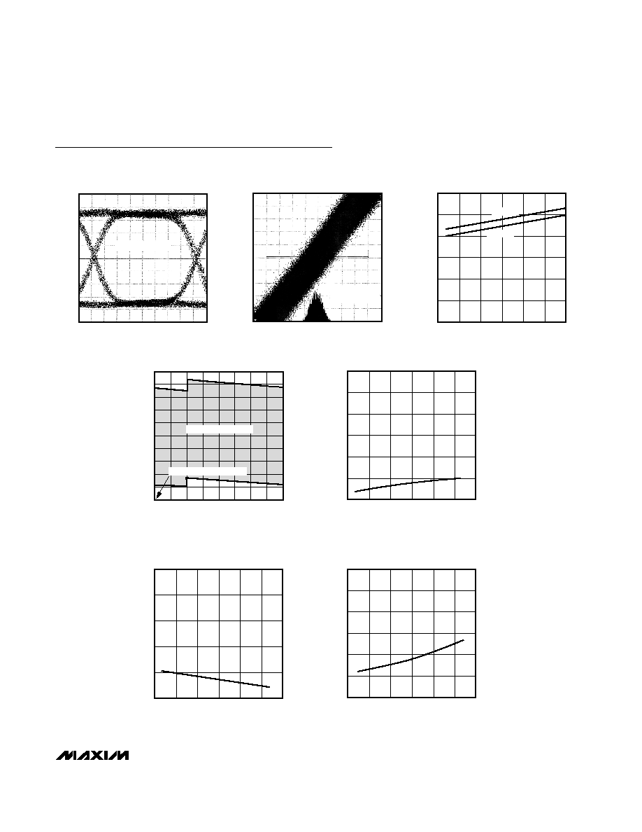
SERIAL-DATA OUTPUT EYE DIAGRAM
MAX3831/2 toc01
50ps/div
2
23
-1 PRBS PATTERN
SERIAL-DATA OUTPUT JITTER
MAX3831/2 toc02
5ps/div
WIDEBAND RMS
JITTER = 2.48ps
0
200
100
400
300
500
600
-50
0
25
-25
50
75
100
SUPPLY CURRENT vs. TEMPERATURE
MAX3831/2 toc03
TEMPERATURE (°C)
SUPPLY CURRENT (mA)
MAX3832
MAX3831
-10
-6
-8
-2
-4
2
0
4
8
6
10
0
0.4
0.6
0.2
0.8
1.0
1.2
1.4
1.6
ELASTIC STORE RANGE
MAX3831/2 toc04
DATA TO RCLKI DELAY AT RESET (ns)
VARIATION OF DATA DELAY AFTER RESET (ns)
CHANNEL ALIGNED TO RCLKI
ERROR-FREE OPERATION
-20
20
0
60
40
80
100
-50
0
25
-25
50
75
100
SERIAL-DATA HOLD TIME
MAX3831/2 toc05
TEMPERATURE (°C)
HOLD TIME (ps)
20
0
60
40
80
100
-50
0
25
-25
50
75
100
SERIAL-DATA SETUP TIME
MAX3831/2 toc06
TEMPERATURE (°C)
SETUP TIME (ps)
0
100
50
200
150
250
300
-50
0
25
-25
50
75
100
MAX3831
PARALLEL CLOCK-TO-DATA OUTPUT
PROPAGATION DELAY vs. TEMPERATURE
MAX3831/2 toc07
TEMPERATURE (°C)
PCLKO TO PDO_ PROPAGATION DELAY (ps)
Typical Operating Characteristics
(V
CC
= +3.3V, T
A
= +25°C, unless otherwise noted.)