General Description
The MAX3867 is a complete, single +3.3V laser driver
for SDH/SONET applications up to 2.5Gbps. The
device accepts differential PECL data and clock inputs
and provides bias and modulation currents for driving a
laser. The synchronizing input latch can be bypassed if
a clock signal is not available.
An automatic power control (APC) feedback loop is
incorporated to maintain a constant average optical
power over temperature and lifetime. The wide modula-
tion current range of 5mA to 60mA and bias current of
1mA to 100mA are easy to program, making this prod-
uct ideal for use in various SDH/SONET applications.
The MAX3867 also provides enable control, a program-
mable slow-start circuit to set the laser turn-on delay,
and a failure-monitor output to indicate when the APC
loop is unable to maintain the average optical power.
The MAX3867 is available in a small 48-pin TQFP pack-
age as well as dice.
Applications
SONET/SDH Transmission Systems
Add/Drop Multiplexers
Digital Cross-Connects
Section Regenerators
2.5Gbps Optical Transmitters
Features
o
Single +3.3V or +5V Power Supply
o
62mA Supply Current at +3.3V
o
Programmable Modulation Current from
5mA to 60mA
o
Programmable Bias Current from 1mA to 100mA
o
Rise/Fall Time < 90ps
o
Automatic Average Power Control with Failure
Monitor
o
Complies with ANSI, ITU, and Bellcore
SDH/SONET Specifications
o
Enable Control
*
Dice are designed to operate over this range, but are tested and
guaranteed at T
A
= +25∞C only. Contact factory for availability.
Ordering Information
MAX3867
+3.3V, 2.5Gbps SDH/SONET Laser Driver
with Automatic Power Control
________________________________________________________________
Maxim Integrated Products
1
EVALUATION KIT
AVAILABLE
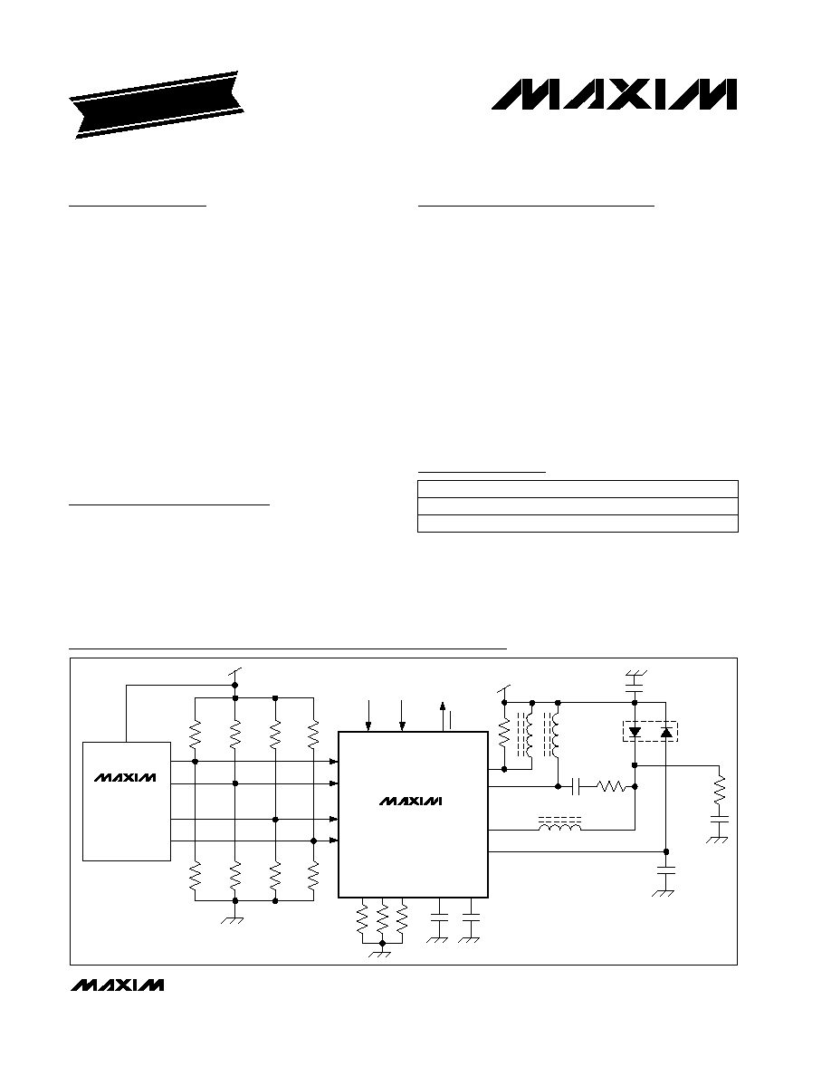
124
124
SERIALIZER
WITH
CLOCK GEN.
124
20
LD
25
+3.3V
+3.3V
0.056
µ
F
1000pF
BIASMAX
LATCH
ENABLE
FAIL
MODSET
APCSET
APCFILT
CLK-
CLK+
DATA-
DATA+
*FERRITE
BEAD
OUT+
BIAS
MD
OUT-
CAPC
124
84.5
84.5
84.5
84.5
MAX3867
MAX3890
Typical Operating Circuit
19-4769; Rev 0a; 9/98
Pin Configuration appears at end of data sheet.
PART
MAX3867ECM
MAX3867E/D
-40∞C to +85∞C
-40∞C to +85∞C
TEMP. RANGE
PIN-PACKAGE
48 TQFP
Dice*
For free samples & the latest literature: http://www.maxim-ic.com, or phone 1-800-998-8800.
For small orders, phone 1-800-835-8769.
MAX3867
+3.3V, 2.5Gbps SDH/SONET Laser Driver
with Automatic Power Control
2
_______________________________________________________________________________________
I
MD
= 1mA
I
MD
= 18µA
90
ENABLE = low (Note 4)
APC open loop, I
BIAS
= 1mA
(Note 3)
900
(Note 2)
(Note 5)
Sourcing 50µA
(Note 6)
APC open loop, I
BIAS
= 100mA
APC open loop
Figure 1
PECL compatible
Sinking 100µA
CONDITIONS
%
-15
15
Monitor-Diode Bias Absolute
Accuracy
ppm/∞C
-480
50
480
Monitor-Diode Bias Setpoint
Stability
µA
18
1000
I
MD
Monitor-Diode DC Current
Range
V
1.5
Monitor-Diode Reverse Bias
Voltage
V
0.1
0.44
TTL Output Low Voltage FAIL
µA
100
I
BIAS-OFF
Bias Off Current
mA
1
100
I
BIAS
mA
62
105
I
CC
Supply Current
Bias Current Range
V
2.4
V
CC
- 0.3
V
CC
TTL Output High Voltage FAIL
V
0.8
TTL Input Low Voltage
(ENABLE, LATCH)
V
2.0
TTL Input High Voltage
(ENABLE, LATCH)
µA
-1
10
I
IN
Clock and Data Input Current
ppm/∞C
230
Bias-Current Stability
%
-15
15
(Note 5)
Bias-Current Absolute Accuracy
mVp-p
200
1600
V
ID
Differential Input Voltage
V
V
CC
- V
CC
- V
CC
-
1.49
1.32
V
ID
/4
V
ICM
Common-Mode Input Voltage
UNITS
MIN
TYP
MAX
SYMBOL
PARAMETER
DC ELECTRICAL CHARACTERISTICS
(V
CC
= +3.14V to +5.5V, T
A
= -40∞C to +85∞C. Typical values are at V
CC
= +3.3V, I
MOD
= 30mA, I
BIAS
= 60mA, and T
A
= +25∞C,
unless otherwise noted.) (Note 1)
Stresses beyond those listed under "Absolute Maximum Ratings" may cause permanent damage to the device. These are stress ratings only, and functional
operation of the device at these or any other conditions beyond those indicated in the operational sections of the specifications is not implied. Exposure to
absolute maximum rating conditions for extended periods may affect device reliability.
Note 1:
Characteristics at -40∞C guaranteed by design and characterization. Dice are tested at T
A
= +25∞C only.
Note 2:
Tested at R
MODSET
= 2.49k
, R
BIASMAX
= 1.69k
, excluding I
BIAS
and I
MOD
.
Note 3:
Voltage on BIAS pin is (V
CC
- 1.6V).
Note 4:
Both the bias and modulation currents will be switched off if any of the current set pins are grounded.
Note 5:
Accuracy refers to part-to-part variation.
Note 6:
Assuming that the laser to monitor-diode transfer function does not change with temperature.
Supply Voltage, V
CC
............................................. -0.5V to +7.0V
Current into BIAS ...........................................-20mA to +150mA
Current into OUT+, OUT- ................................-20mA to +100mA
Current into MD.....................................................-5mA to +5mA
Voltage at DATA+, DATA-, CLK+, CLK-,
ENABLE, LATCH, FAIL, SLWSTRT.........-0.5V to (V
CC
+ 0.5V)
Voltage at APCFILT, CAPC, MODSET,
BIASMAX, APCSET ...........................................-0.5V to +3.0V
Voltage at OUT+, OUT-.............................+1.5V to (V
CC
+ 1.5V)
Voltage at BIAS .........................................+1.0V to (V
CC
+ 0.5V)
Current into FAIL ...............................................-10mA to +30mA
Continuous Power Dissipation (T
A
= +85∞C)
TQFP (derate 20.8mW/∞C above +85∞C) ...................1354mW
Storage Temperature Range .............................-65∞C to +165∞C
Operating Junction Temperature Range ...........-55∞C to +150∞C
Processing Temperature (die) .........................................+400∞C
Lead Temperature (soldering, 10sec) .............................+300∞C
ABSOLUTE MAXIMUM RATINGS
MAX3867
+3.3V, 2.5Gbps SDH/SONET Laser Driver
with Automatic Power Control
_______________________________________________________________________________________
3
AC ELECTRICAL CHARACTERISTICS
(V
CC
= +3.14V to +5.5V, load as shown in Figure 2, T
A
= -40∞C to +85∞C. Typical values are at V
CC
= +3.3V, I
MOD
= 30mA, and T
A
=
+25∞C.) (Note 7)
Note 7:
AC characteristics are guaranteed by design and characterization.
Note 8:
Measured with 622Mbps 0-1 pattern, LATCH = high.
Note 9:
PWD = (wider pulse - narrower pulse) / 2.
Note 10:
See
Typical Operating Characteristics for worst-case distribution.
I
MOD
= 5mA
250
79
LATCH = high, Figure 3
LATCH = high, Figure 3
20% to 80% (Note 8)
ps
69
(Note 8)
20% to 80% (Note 8)
ENABLE = low (Note 4)
I
MOD
= 60mA
(Note 6)
Jitter BW = 12kHz to 20MHz, 0-1 pattern
(Notes 8, 9)
CONDITIONS
t
R
Output Rise Time
ps
ps
p-p
7
20
Jitter Generation
ps
9
50
PWD
Pulse-Width Distortion
mA
5
60
I
MOD
Modulation-Current Range
ps
100
t
H
ps
100
t
SU
Input Latch Setup Time
Input Latch Hold Time
bits
80
Maximum Consecutive Identical
Digits
ns
250
Enable/Start-Up Delay
%
±15
Output Aberrations
79
t
F
Output Fall Time
µA
200
I
MOD-OFF
Modulation-Off Current
ppm/∞C
-480
-50
480
Modulation-Current Stability
%
-15 15
Modulation-Current Absolute
Accuracy
88
(Note 10)
UNITS
MIN
TYP
MAX
SYMBOL
PARAMETER
MAX3867ECM
MAX3867C/D
MAX3867ECM
MAX3867C/D
MAX3867
+3.3V, 2.5Gbps SDH/SONET Laser Driver
with Automatic Power Control
4
_______________________________________________________________________________________
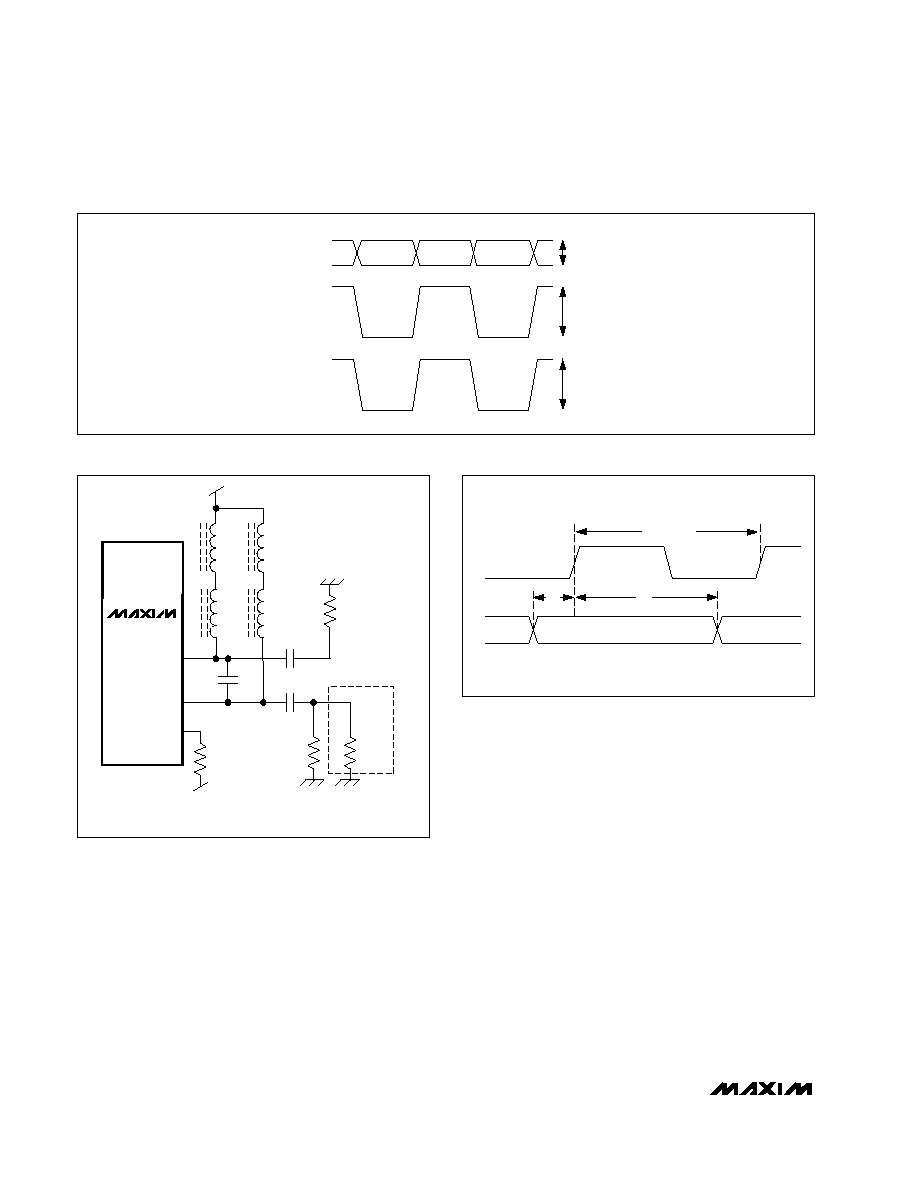
DATA+
DATA-
(DATA+) - (DATA-)
I
OUT
+
100mV MIN
800mV MAX
200mVp-p MIN
1600mVp-p MAX
I
MOD
Figure 1. Required Input Signal and Output Polarity
CLK
DATA
t
CLK
= 402ps
t
SU
t
H
Figure 3. Setup/Hold Time Definition
0.056
µ
F
0.5pF
*
* TO COMPENSATE PACKAGE LEADS, NOT USED FOR DIE.
OUT+
BIAS
OUT-
A
B
A
A, B ARE SMD FERRITE BEADS
B = BLM11A601S MURATA ELECTRONICS
A = BLM21A102S MURATA ELECTRONICS
B
V
CC
50
15
OSCILLOSCOPE
50
25
0.056
µ
F
V
CC
MAX3867
Figure 2. Output Termination for Characterization
MAX3867
+3.3V, 2.5Gbps SDH/SONET Laser Driver
with Automatic Power Control
_______________________________________________________________________________________
5
26mV
/div
50ps/div
ELECTRICAL EYE DIAGRAM
MAX3867-04a
PATTERN = 2
13
- 1 + 80 CID
I
MOD
= 30mA
48-TQFP
0.010
0.012
0.014
0.016
0.018
0.020
0.022
4
18
11
25
32
39
46
53
60
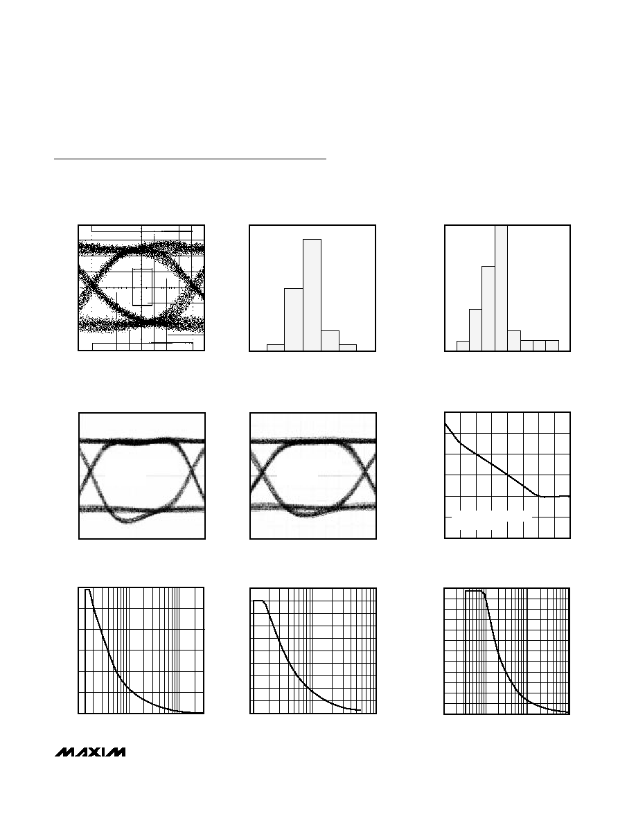
RANDOM JITTER vs. I
MOD
MAX3867 toc05
I
MOD
(mA)
RANDOM JITTER (UIp-p)
JITTER BW = 12kHz to 20MHz
1-0 PATTERN
55mV
/div
50ps/div
ELECTRICAL EYE DIAGRAM
MAX3867-05a
PATTERN = 2
13
- 1 + 80 CID
I
MOD
= 60mA
48-TQFP
120
0
1
10
100
300
I
BIASMAX
vs. R
BIASMAX
MAX3867-06
R
BIASMAX
(k
)
I
BIASMAX
(mA)
40
80
100
20
60
100
0
1
10
100
I
MOD
vs. R
MODSET
20
10
MAX3867-07
R
MODSET
(k
)
I
MOD
(mA)
40
30
60
70
50
80
90
1.2
0
0.1
1
10
100
I
MD
vs. R
APCSET
0.4
MAX3867-08
R
APCSET
(k
)
I
MD
(mA)
0.6
0.8
1.0
1.1
0.3
0.2
0.1
0.5
0.7
0.9
Typical Operating Characteristics
(V
CC
= +3.3V, load as shown in Figure 2, T
A
= +25∞C, unless otherwise noted.)
EYE DIAGRAM
(2.488Gbps, 1300nm FP LASER,
1.87GHz FILTER, 48-TQFP)
MAX3867-01
50ps/div
0
20
10
40
30
50
60
80
88
48-TQFP
I
MOD
= 30mA
MEAN = 88ps
= 3.0ps
92
96
84
100
TYPICAL DISTRIBUTION OF FALL TIME
MAX3867-02a
FALL TIME (ps)
PERCENT IN UNITS (%)
0
20
15
10
5
30
25
40
35
106 108
112
48-TQFP
I
MOD
= 30mA
V
CC
= +3.14V
T
A
= +85∞C
MEAN = 111.6ps
= 2.9ps
114 116 118
110
120 122
DISTRIBUTION OF FALL TIME
(WORST-CASE CONDITIONS)
MAX3867-03a
FALL TIME (ps)
PERCENT IN UNITS (%)