General Description
The MAX3867 evaluation kit (EV kit) is an assembled
demonstration board that provides optical or electrical
evaluation of the MAX3867.
The EV kit is composed of two independent sections on
the PC board. The output of the electrical evaluation
section is interfaced to an SMA connector, which can
be connected to a 50
terminated oscilloscope. The
output of the optical evaluation section is configured for
attachment to a laser/monitor diode.
Features
o Fully Assembled and Tested
o +3.3V to +5.0V Operation
o Input Termination Provided On-Board
Evaluates: MAX3867
MAX3867 Evaluation Kit
________________________________________________________________ Maxim Integrated Products
1
19-1420; Rev 1; 6/00
Electrical Component List
PART
MAX3867EVKIT
-40∞C to +85∞C
TEMP. RANGE
IC PACKAGE
48 TQFP
Ordering Information
1k
ferrite beads (0805)
Murata BLM21A102S
2
L7, L13
2-pin headers (0.1in center)
Digi-Key S1012-36-ND
2
JU4, JU5
Shunts
Digi-Key S9000-ND
2
JU4, JU5
SMA edge-mount connectors
EFJohnson 142-0701-801 or
Digi-Key J502-ND
5
J5≠J9
LED
Digi-Key P363-ND
1
D3
1000pF ±10% ceramic capacitor (0402)
1
C43
0.01µF ±10% ceramic capacitors
(0603)
2
C41, C45
10µF ±20% tantalum (16V) capacitor
AVX TAJC106M016
1
C40
DESIGNATION
0.056µF ±10% ceramic capacitors
(0603)
2
C37, C39
0.1µF ±10% ceramic capacitors (0603)
5
C26, C27, C29,
C30, C34
Do not install.
5
C14, C21, C31,
C33, C44
DESCRIPTION
QTY
0.22µF ±10% ceramic capacitor (0603)
1
C42
Do not install.
1
R37
110
±1% resistor (0603)
1
R34
124
±1% resistors (0402)
4
R28, R29, R32,
R33
84.5
±1% resistors (0402)
4
R25, R26, R30,
R31
1k
±1% resistor (0603)
1
R23
1.5k
±1% resistors (0603)
3
R5, R22, R47
DESIGNATION
DESCRIPTION
QTY
1.2µH inductor
Coilcraft 1008LS-122XKBC
1
L9
R38, R49
2
49.9
±1% resistors (0402)
R40
1
100k
variable resistor
Bournes or Digi-Key 3296W-104-ND
R41
1
50k
variable resistor
Bournes or Digi-Key 3296W-503-ND
R42
1
200k
variable resistor
Bournes or Digi-Key 3296W-204-ND
R43, R45
2
0
resistors (0603)
R46
1
15
±1% resistor (0603)
U2
1
MAX3867ECM (48-pin TQFP)
U3
1
MAX495ESA
600
ferrite beads (0603)
Murata BLM11A601SPT
2
L10, L11
TP2, TP3, TP8,
TP10≠TP13,
VCC1, GND1
9
Test points
Digi-Key 5000K-ND
TP17, TP18
2
Do not install.
None
1
MAX3867 EV kit circuit board (Rev D)
0.01µF ±10% ceramic capacitors
(0402)
4
C24, C25, C28,
C32
R44
1
24.9
±1% resistor (0402)
None
1
MAX3867 data sheet
For free samples and the latest literature, visit www.maxim-ic.com or phone 1-800-998-8800.
For small orders, phone 1-800-835-8769.
Q2
PNP transistor (SOT23)
Zetex FMMT591A ("91A" marking)
1
Quick Start
Electrical Evaluation
In the electrical configuration, an automatic power con-
trol (APC) test circuit is included to emulate a semicon-
ductor laser with a monitor photodiode. Monitor diode
(MD) current is provided by Q2, which is controlled by
an operational amplifier (U3). The APC test circuit, con-
sisting of U3 and Q2, applies the simulated MD current
(the laser bias current divided by 100) to the MD pin of
the MAX3867. To ensure proper operation in the electri-
cal configuration, set up the evaluation board as fol-
lows:
1) If data is to be latched, remove the shunt from JU4
to enable the input clock; otherwise, leave the shunt
in place.
EFJohnson
Evaluates: MAX3867
MAX3867 Evaluation Kit
2
_______________________________________________________________________________________
600
ferrite bead (0603)
Murata BLM11HA601SPT
1
L2
0
resistor (0603)
1
L3
1k
ferrite bead (0805)
Murata BLM21A102S
1
L1
Shunts
Digi-Key S9000-ND
2
JU1, JU2
2-pin headers (0.1in center)
Digi-Key S1012-36-ND
2
JU1, JU2
0.1µF ±10% ceramic capacitors (0603)
5
C10≠C13, C23
SMA edge-mount connectors
EFJohnson 142-0701-801 or
Digi-Key J502-ND
4
J1≠J4
LED
Digi-Key P363-ND
1
D1
0.01µF ±10% ceramic capacitors
(0603)
3
C20, C22, C36
10µF ±20% tantalum (16V) capacitor
AVX TAJC106M016
1
C19
0.056µF ±10% ceramic capacitor
(0603)
1
C7
DESIGNATION
1000pF ±10% ceramic capacitor
(0402)
1
C6
Do not install.
6
C5, C8, C9,
C15, C18, C35
0.01µF ±10% ceramic capacitors
(0402)
6
C1≠C4, C17,
C38
DESCRIPTION
QTY
R16
1
100k
variable resistor
Bournes or Digi-Key 3296W-104-ND
200k
variable resistor
Bournes or Digi-Key 3296W-204-ND
1
R15
R18
1
110
±1% resistor (0603)
R19
1
Do not install.
R20
1
27.4
±1% resistor (0402)
R21
1
49.9
±1% resistor (0402)
R27
1
24.9
±1% resistor (0402)
R35, R48
2
0
resistors (0603)
50k
variable resistor
Bournes or Digi-Key 3296W-503-ND
1
R14
124
±1% resistors (0402)
4
R8, R9, R12,
R13
84.5
±1% resistors (0402)
4
R6, R7, R10,
R11
1.0k
±1% resistor (0603)
1
R3
1.5k
±1% resistors (0603)
2
R1, R2
1.2µH Inductor
Coilcraft 1008LS-122XKBC
1
L4
TP15, TP16
2
Do not install.
TP1, TP4, TP5,
TP6, TP14,
VCC, GND
7
Test points
Digi-Key 5000K-ND
DESIGNATION
DESCRIPTION
QTY
Optical Component List
SUPPLIER
PHONE
FAX
AVX
803-946-0690
803-626-3123
Coilcraft
847-639-6400
847-639-1469
402-474-4800
402-474-4858
Zetex
516-543-7100
516-864-7630
Component Suppliers
Digi-Key
218-681-6674
218-681-3380
Murata
814-237-1431
814-238-0490
600
ferrite beads (0603)
Murata BLM11A601SPT
2
L5, L6
U1
1
MAX3867ECM (48-pin TQFP)
R36
1
43.2
±1% resistor (0402)
0.22µF ±10% ceramic capacitor (0805)
1
C16

2) Remove the shunt from JU5 to enable the outputs.
Note: When performing the following resistance checks,
manually set the ohmmeter to a high range to avoid for-
ward biasing the on-chip ESD protection diodes.
3) Adjust R41, the MOD potentiometer, for 10k
resis-
tance between pins 1 and 3 (test point 3 and
ground).
4) Adjust R42, the BIAS potentiometer, for 10k
resis-
tance between pins 1 and 3 (test point 2 and
ground).
5) Adjust R40, the APC potentiometer, for 10k
resis-
tance between pins 1 and 3 (test point 8 and ground).
6) Apply a differential input signal (max amplitude
800mV per side) to J7 and J8 (DATA+ and DATA-).
7) If the latch is enabled, apply a differential clock sig-
nal (max amplitude
800mV per side) to J5 and J6
(CLK+ and CLK-).
8) Attach a high-speed oscilloscope with 50
inputs
to J9.
9) Power up the board with a +3.3V supply.
10) Adjust R42 until the desired laser bias current is
achieved:
11) Adjust R41 until the desired laser modulation cur-
rent is achieved:
Optical Evaluation
For optical evaluation of the MAX3867, configure the EV
kit as follows:
1) If data is to be latched, remove the shunt from JU1
to enable the input clock; otherwise, leave the shunt
in place.
2) Remove the shunt from JU2 to enable the outputs.
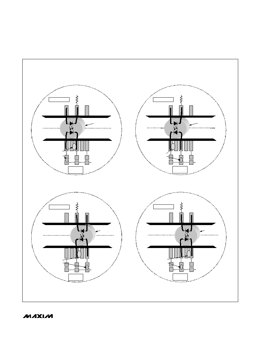
3) The EV kit is designed to allow connection of a vari-
ety of possible laser/monitor diode pin configura-
tions. Connect a TO-header-style laser with MD
(Figure 1) as follows:
∑
Keeping its leads as short as possible, connect
the laser diode to two of the three pads in the
cutout portion on the top (component) side of
the PC board. Solder the laser diode cathode to
the center pad, and solder the anode to either
of the other two pads (they are both connected
to V
CC
).
∑
Connect the monitor photodiode to two of the
five pads on the bottom (solder) side of the PC
board, directly below the laser diode pads.
Three of these pads (the middle and outside
positions) are initially not connected. The other
two pads are connected to V
CC
. Solder the
anode and cathode of the monitor photodiode
to any two of the three pads that are not con-
nected. Then connect the anode to the MD pin
by shorting the corresponding solder jumper
(Figure 1). Connect the cathode to V
CC
by using
solder to bridge to an adjacent V
CC
pad.
Note: When performing resistance checks, manually
set the ohmmeter to a high range to avoid for-
ward biasing the on-chip ESD protection diodes.
4) Adjust R14, the MOD potentiometer, for maximum
resistance between pins 1 and 3 (test point 5 and
ground).
5) Adjust R15, the BIAS potentiometer, for maximum
resistance between pins 1 and 3 (test point 4 and
ground).
6) Adjust R16, the APC potentiometer, for desired opti-
cal power. (Refer to the Design Procedure section
of the MAX3867 data sheet.)
7) Apply a differential input signal (
800mV per side)
to J1 and J2 (DATA+ and DATA-).
8) Apply a differential clock signal (
800mV per side)
to J3 and J4 (CLK+ and CLK-).
9) Attach the laser diode fiber connector to an opti-
cal/electrical converter.
10) Power up the board with a +3.3V supply.
11) Adjust R15 until the LED (D1) is no longer illuminat-
ed. Optical power can be observed on an oscillo-
scope connected to an optical/electrical converter.
12) Adjust R14 until the desired optical amplitude is
achieved. Optical amplitude can be observed on
an oscilloscope connected to an optical/electrical
converter.
I
MOD
=
Signal Amplitude (Volts)
25
I
BIAS
TP13
TP12
=
V
- V
15
Evaluates: MAX3867
MAX3867 Evaluation Kit
_______________________________________________________________________________________
3
Evaluates: MAX3867
MAX3867 Evaluation Kit
4
_______________________________________________________________________________________
Adjustment and Control Descriptions (see Quick Start first)
Electrical Output
Electrical Output SMA
--
OPTICAL
FUNCTION
NAME
Refer to the Design section of the MAX3867 data sheet. Set APC cur-
rent, then increase bias current until LED goes off (LED is illuminated
when the APC loop is open, and off when the APC loop is closed).
Fail Indicator
D1
TTL low level indicates a failure in the APC loop.
Fail Indicator
TP1
ELECTRICAL
JU4
JU5
J8
R41
R42
R40
TP10
D3
For closed-loop operation, R16 or R40 adjusts the MD current level.
APC
R16
Adjusts the laser bias current. In open-loop mode, R15 or R42 adjusts
the laser bias current. In closed-loop operation, R15 or R42 adjusts the
maximum laser bias current.
BIAS
R15
Adjusts the laser modulation current.
MOD
R14
Enables/disables the output currents. Shunt to disable the part.
Remove shunt for normal operation.
OUTPUT DISABLE
JU2
Enables/disables the clock input. Shunt for direct data transmission.
Remove shunt to enable clock input.
CLOCK DISABLE
JU1
COMPONENT
Evaluates: MAX3867
MAX3867 Evaluation Kit
_______________________________________________________________________________________
5
Figure 1. Attachment of Laser Diode/Monitor Diode to MAX3867 EV Kit
TOP OF PC BOARD
R20
V
CC
V
CC
TO-46 CAN
LASER/PHOTODIODE
PAIR
LD
PD
TO MD
V
CC
V
CC
SOLDER
BRIDGES
BOTTOM OF
PC BOARD
CONFIGURATION 1
TOP OF PC BOARD
R20
V
CC
V
CC
TO-46 CAN
LASER/PHOTODIODE
PAIR
LD
PD
V
CC
V
CC
TO MD
BOTTOM OF
PC BOARD
SOLDER
BRIDGES
CONFIGURATION 2
TOP OF PC BOARD
R20
V
CC
V
CC
TO-46 CAN
LASER/PHOTODIODE
PAIR
LD
PD
V
CC
V
CC
TO MD
BOTTOM OF
PC BOARD
SOLDER
BRIDGES
CONFIGURATION 3
R20
V
CC
V
CC
TOP OF PC BOARD
LD
TO-46 CAN
LASER/PHOTODIODE
PAIR
PD
V
CC
V
CC
TO MD
BOTTOM OF
PC BOARD
SOLDER
BRIDGES
CONFIGURATION 4