 | ÐлекÑÑоннÑй компоненÑ: MAX4024 | СкаÑаÑÑ:  PDF PDF  ZIP ZIP |
MAX4023-6 DS
General Description
The MAX4023MAX4026 family of voltage feedback
multiplexer-amplifiers combine low-glitch switching and
excellent video specifications with fixed or settable
gain. The MAX4024/MAX4026 are triple and quad 2:1
multiplexers, respectively, with amplifiers that have a
fixed gain of +2. The MAX4023/MAX4025 are triple and
quad 2:1 multiplexers, respectively, with adjustable
gain amplifiers optimized for unity-gain stability. All
devices have 25ns channel switching time and low
10mV
P-P
switching transients, making them ideal for
high-speed video-switching applications. These
devices operate from a single +4.5V to +11V supply or
from dual supplies of ±2.25V to ±5.5V, and feature an
input common-mode voltage range that extends to the
negative supply rail. A low-power disable mode places
the output in a high-impedance state.
The MAX4023/MAX4025 have -3dB bandwidths of
260MHz and up to 330V/µs slew rates with a settable
gain to equalize long cable runs. The MAX4024/
MAX4026, with 200MHz -3dB bandwidths and 363V/µs
slew rates, have a fixed gain of +2 for driving short
back-terminated cables. The MAX4023/MAX4025 inter-
nal amplifiers maintain an open-loop output impedance
of only 18
over the full output voltage range, and mini-
mize the gain error and bandwidth changes under
loads typical of most Rail-to-Rail
®
amplifiers. These
devices are ideal for broadcast video applications with
differential gain and phase errors of 0.07% and 0.07°,
respectively.
Applications
Set-Top Boxes
In-Car Navigation/Entertainment
Servers
Security Systems
Video Projectors
Notebook Computers
Broadcast Video
Video Crosspoint Switching
Features
o Single +5V or Dual ±5V Operation
o 260MHz -3dB Bandwidth (MAX4023/MAX4025)
o 200MHz -3dB Bandwidth (MAX4024/MAX4026)
o 363V/µs Slew Rate (MAX4024/MAX4026)
o 25ns Channel Switching Time
o Ultra-Low 20mV
P-P
Switching Transient
o 0.012%/0.05° Differential Gain/Phase Error
o Input Common-Mode Range Includes Negative
Rail (MAX4023/MAX4025)
o Low-Power Disable Mode
o Available in Space-Saving 14-Pin TSSOP and
16-Pin QSOP Packages
MAX4023MAX4026
Triple and Quad, 2:1 Video Multiplexer-
Amplifiers with Fixed and Settable Gain
________________________________________________________________ Maxim Integrated Products
1
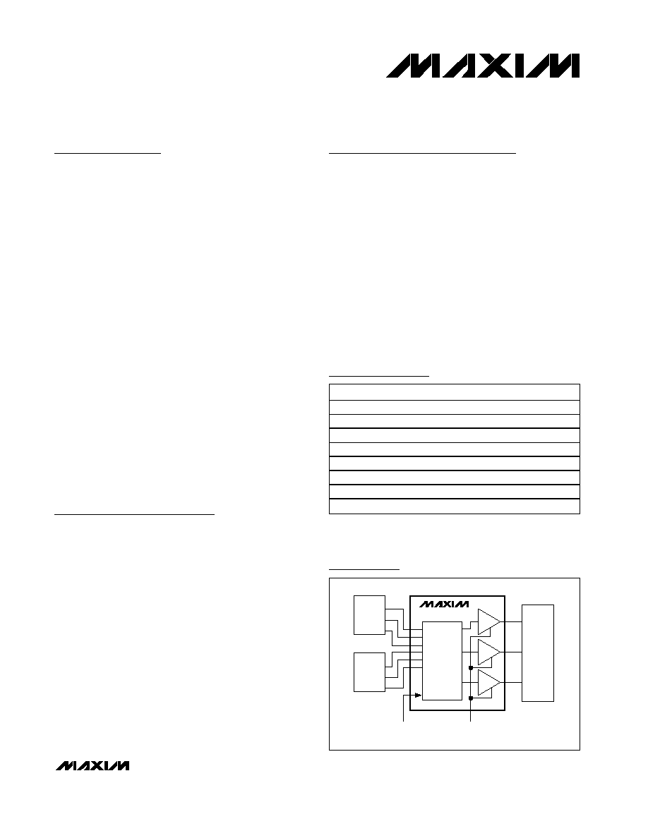
VIDEO
SOURCE
1
R
G
B
R
G
B
TRIPLE
2:1
MUX
DISPLAY
SOURCE
SELECT
EN
R
G
B
VIDEO
SOURCE
2
MAX4024
x 2
x 2
x 2
Typical Operating Circuit
19-2758; Rev 0; 1/03
For pricing, delivery, and ordering information, please contact Maxim/Dallas Direct! at
1-888-629-4642, or visit Maxim's website at www.maxim-ic.com.
Ordering Information
PART
TEMP RANGE
PIN-PACKAGE
MAX4023EEE
-40°C to +85°C
16 QSOP
MAX4023ESE
-40°C to +85°C
16 Narrow SO
MAX4024EUD
-40°C to +85°C
14 TSSOP
MAX4024ESD
-40°C to +85°C
14 Narrow SO
MAX4025EUP
-40°C to +85°C
20 TSSOP
MAX4025EWP
-40°C to +85°C
20 Wide SO
MAX4026EUP
-40°C to +85°C
20 TSSOP
MAX4026EWP
-40°C to +85°C
20 Wide SO
Selector Guide and Pin Configurations appear at end of data
sheet.
Rail-to-Rail is a registered trademark of Nippon Motorola, Ltd.
MAX4023MAX4026
Triple and Quad, 2:1 Video Multiplexer-
Amplifiers with Fixed and Settable Gain
2
_______________________________________________________________________________________
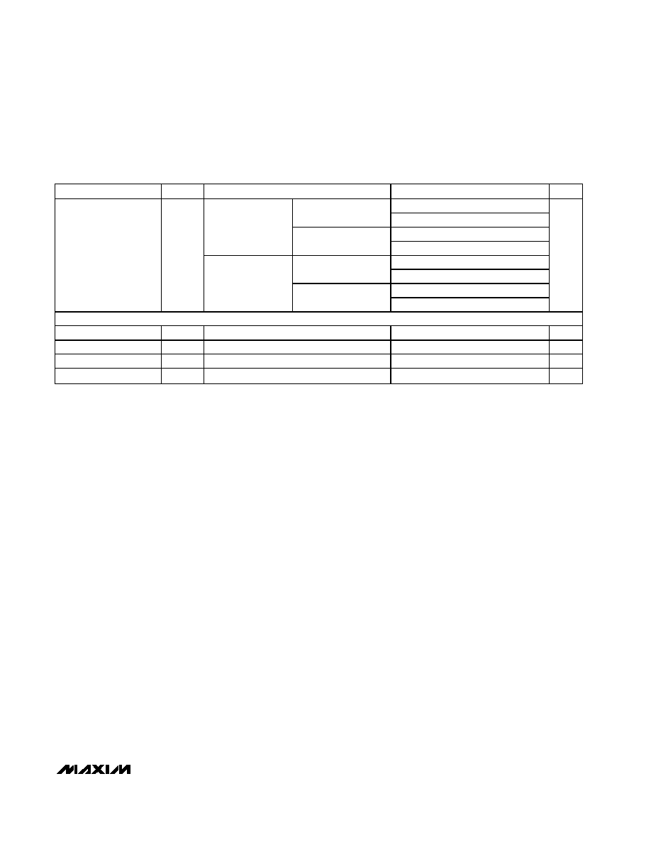
ABSOLUTE MAXIMUM RATINGS
Stresses beyond those listed under "Absolute Maximum Ratings" may cause permanent damage to the device. These are stress ratings only, and functional
operation of the device at these or any other conditions beyond those indicated in the operational sections of the specifications is not implied. Exposure to
absolute maximum rating conditions for extended periods may affect device reliability.
Supply Voltage (V
CC
to V
EE
) ..................................................12V
IN_A, IN_B, FB_ ...............................(V
EE
- 0.3V) to (V
CC
+ 0.3V)
REF, EN, A/B ....................................(V
EE
- 0.3V) to (V
CC
+ 0.3V)
Current Into IN_A, IN_B, FB_ ............................................±20mA
Short-Circuit Duration (OUT_ to GND or V
EE
) ............Continuous
Short-Circuit Duration (OUT_ to V
CC
)..............................(Note 1)
Continuous Power Dissipation (T
A
= +70°C)
14-Pin TSSOP (derate 9.1mW/°C above +70°C) .........727mW
14-Pin Narrow SO (derate 8.3mW/°C above +70°C) ...667mW
16-Pin QSOP (derate 8.3mW/°C above +70°C)...........667mW
16-Pin Narrow SO (derate 8.7mW/°C above +70°C) ...696mW
20-Pin TSSOP (derate 10.9mW/°C above +70°C) .......879mW
20-Pin Wide SO (derate 10mW/°C above +70°C)........800mW
Operating Temperature Range ...........................-40°C to +85°C
Junction Temperature ......................................................+150°C
Storage Temperature Range .............................-65°C to +150°C
Lead Temperature (soldering, 10s) .................................+300°C
Note 1: Do not short OUT_ to V
CC
.
DC ELECTRICAL CHARACTERISTICS--Dual Supply
(V
CC
= +5V, V
EE
= -5V, R
L
=
, EN = +5V, V
CM
= REF = OUT_ = 0V, T
A
= T
MIN
to T
MAX
, unless otherwise noted. Typical values are at
T
A
= +25°C.) (Note 2)
PARAMETER
SYMBOL
CONDITIONS
MIN
TYP
MAX
UNITS
O p er ati ng S up p l y V ol tag e Range
V
S
Guaranteed by PSRR
±2.25
±5.5
V
MAX4023/MAX4024
25
36
Quiescent Supply Current
I
S
OUT = 0V
MAX4025/MAX4026
34
48
mA
MAX4023/MAX4024
3.6
6
Disable Supply Current
EN = 0V
MAX4025/MAX4026
4.4
6
mA
MAX4023/MAX4025, inferred from CMRR
V
EE
V
CC
- 2.8
Input Voltage Range
V
IN
MAX4024/MAX4026, inferred from A
VCL
V
EE
+ 2.9
V
CC
- 2.8
V
MAX4023/MAX4025
±0.5
±15
Input Offset Voltage
V
OS
MAX4024/MAX4026
±1
±18
mV
MAX4023/MAX4025
±1
Input Offset Voltage Matching
V
OS
MAX4024/MAX4026
±1.5
mV
MAX4023/MAX4025
15
Input Offset Voltage Drift
TC
VOS
MAX4024/MAX4026
23
µV°C
Input Bias Current
I
B
4
14
µA
Input Offset Current
I
OS
MAX4023/MAX4025
±0.1
±2
µA
Differential Input Resistance
R
IND
M AX 4023/M AX 4025, - 10m V < V
IN D
< + 10m V 50
k
MAX4023/MAX4025, common mode
4.5
Input Resistance
R
IN
MAX4024/MAX4026, single ended
4.5
M
Open loop
18
MAX4023/MAX4025
Cl osed l oop , A
VC L
= +1
0.025
Output Resistance
R
OUT
MAX4024/MAX4026
0.15
MAX4023MAX4026
Triple and Quad, 2:1 Video Multiplexer-
Amplifiers with Fixed and Settable Gain
_______________________________________________________________________________________
3
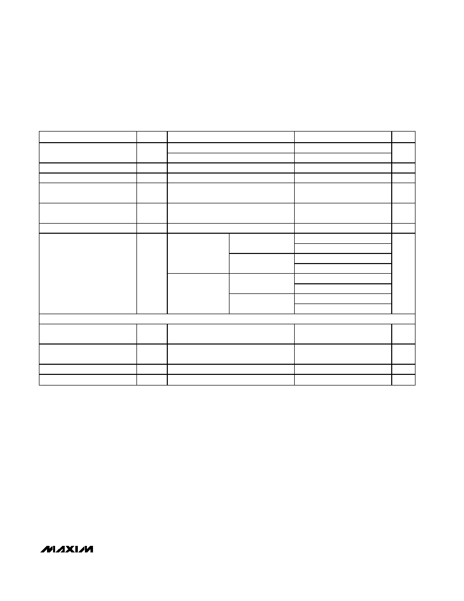
DC ELECTRICAL CHARACTERISTICS--Dual Supply (continued)
(V
CC
= +5V, V
EE
= -5V, R
L
=
, EN = +5V, V
CM
= REF = OUT_ = 0V, T
A
= T
MIN
to T
MAX
, unless otherwise noted. Typical values are at
T
A
= +25°C.) (Note 2)
PARAMETER
SYMBOL
CONDITIONS
MIN
TYP
MAX
UNITS
MAX4023/MAX4025, EN = 0V
75
Disable Output Resistance
R
OUT
MAX4024/MAX4026, EN = 0V
1
k
Power-Supply Rejection Ratio
PSRR
±2.25V < V
S
< ±5.5V
50
64
dB
Common-Mode Rejection Ratio
CMRR
M AX4023/M AX4025, V
E E
< V
C M
< V
C C
- 2.8V
50
68
dB
Open-Loop Gain
A
VOL
MAX4023/MAX4025, R
L
= 150
,
-4.3V < V
OUT
< +4.3V
70
85
dB
Voltage Gain
A
VCL
MAX4024/MAX4026, R
L
= 150
,
V
EE
+ 2.9V < V
IN
< V
CC
- 2.8V
5.5
6.0
6.5
dB
Gain Matching
A
VCL
MAX4024/MAX4026
1
%
V
C C
- 0.7
V
CC
- 0.5
R
L
= 150
V
EE
+ 0.5 V
EE
+ 0.7
V
CC
- 1.2
V
CC
- 0.8
MAX4023/MAX4025
R
L
= 75
V
EE
+ 0.8 V
EE
+ 1.2
V
C C
- 0.7
V
C C
- 0.5
R
L
= 150
V
EE
+ 0.3 V
EE
+ 0.7
V
CC
- 1.2
V
CC
- 0.8
Output Voltage Swing
V
OUT
MAX4024/MAX4026
R
L
= 75
V
EE
+ 0.5 V
EE
+ 1.2
V
LOGIC INPUT CHARACTERISTICS
Logic-Low Threshold
V
IL
EN, A/B
V
CC
- 3.85
V
Logic-High Threshold
V
IH
EN, A/B
V
CC
- 3.3
V
Logic-Low Input Current
I
IL
EN, A/B; EN or A/B = 0V
5
10
µA
Logic-High Input Current
I
IH
EN, A/B; EN or A/B = V
CC
2
8
µA
MAX4023MAX4026
Triple and Quad, 2:1 Video Multiplexer-
Amplifiers with Fixed and Settable Gain
4
_______________________________________________________________________________________
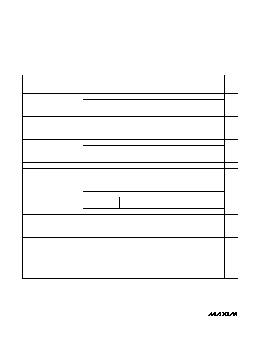
DC ELECTRICAL CHARACTERISTICS--Single Supply
(V
CC
= +5V, V
EE
= 0V, R
L
=
, EN = +5V, V
CM
= REF = OUT = 0.5V, T
A
= T
MIN
to T
MAX
, unless otherwise noted. Typical values are at
T
A
= +25°C.) (Note 2)
PARAMETER
SYMBOL
CONDITIONS
MIN
TYP
MAX
UNITS
O p er ati ng S up p l y
V ol tag e Rang e
V
S
Guaranteed by PSRR
4.5
11
V
MAX4023/MAX4024, OUT = 0V
19
32
Quiescent Supply
Current
I
S
MAX4025/MAX4026, OUT = 0V
31
43
mA
MAX4023/MAX4024, EN = 0V
3.3
6
Disable Supply Current
MAX4025/MAX4026, EN = 0V
3.9
6
mA
MAX4023/MAX4025, inferred from CMRR
V
EE
V
CC
- 2.8
Input Voltage Range
V
IN
MAX4024/MAX4026, inferred from A
VCL
V
EE
+ 0.28
V
CC
- 2.8
V
MAX4023/MAX4025
±1
±18
Input Offset Voltage
V
OS
MAX4024/MAX4026
±3
±20
mV
MAX4023/MAX4025
±1
Input Offset Voltage
Matching
V
OS
MAX4024/MAX4026
±1.5
mV
MAX4023/MAX4025
9
Input Offset Voltage Drift
TC
VOS
MAX4024/MAX4026
13
µV°C
Input Bias Current
I
B
4.5
14
µA
Input Offset Current
I
OS
MAX4023/MAX4025
±0.1
±2
µA
Differential Input
Resistance
R
IND
M AX 4023/M AX 4025, - 10m V < V
IN D
< + 10m V 50
k
MAX4023/MAX4025, common mode
4.5
Input Resistance
R
IN
MAX4024/MAX4026, single ended
4.5
M
Open loop
18
MAX4023/MAX4025
C l osed l oop , A
V C L
= + 1
0.025
Output Resistance
R
OUT
MAX4024/MAX4026
0.15
MAX4023/MAX4025, EN = 0V
75
Disable Output
Resistance
R
OUT
MAX4024/MAX4026, EN = 0V
1
k
Power-Supply Rejection
Ratio
PSRR
±4.5V < V
S
< ±11V
50
64
dB
Common-Mode
Rejection Ratio
CMRR
MAX4023/MAX4025, V
EE
< V
CM
< V
CC
- 2.8V
50
91
dB
Open-Loop Gain
A
VOL
M AX 4023/M AX 4025, R
L
= 150
,
0.3V < V
OU T
< 4.3V
70
85
dB
Voltage Gain
A
VCL
MAX4024/MAX4026, R
L
= 150
,
V
EE
+ 0.28V < V
IN
< V
CC
- 2.8V
5.5
6.0
6.5
dB
Gain Matching
A
VCL
MAX4024/MAX4026
1
%
MAX4023MAX4026
Triple and Quad, 2:1 Video Multiplexer-
Amplifiers with Fixed and Settable Gain
_______________________________________________________________________________________
5
DC ELECTRICAL CHARACTERISTICS--Single Supply (continued)
(V
CC
= +5V, V
EE
= 0V, R
L
=
, EN = +5V, V
CM
= REF = OUT = 0.5V, T
A
= T
MIN
to T
MAX
, unless otherwise noted. Typical values are at
T
A
= +25°C.) (Note 2)
PARAMETER
SYMBOL
CONDITIONS
MIN
TYP
MAX
UNITS
V
CC
- 1.1
V
CC
- 0.5
R
L
= 150
to GND
V
E E
+ 0.03
V
E E
+ 0.175
V
CC
- 1.1
V
CC
- 0.8
MAX4023/MAX4025
R
L
= 75
to GND
V
E E
+ 0.03
V
E E
+ 0.175
V
CC
- 1.1
V
CC
- 0.5
R
L
= 150
to GND
V
E E
+ 0.03
V
E E
+ 0.09
V
CC
- 1.1
V
CC
- 0.8
Output Voltage Swing
V
OUT
MAX4024/MAX4026
R
L
= 75
to GND
V
E E
+ 0.04
V
E E
+ 0.08
V
LOGIC INPUT CHARACTERISTICS
Logic-Low Threshold
V
IL
EN, A/B
V
CC
- 3.85
V
Logic-High Threshold
V
IH
EN, A/B
V
CC
- 3.3
V
Logic-Low Input Current
I
IL
EN, A/B; EN or A/B = 0V
5
10
µA
Logic-High Input
I
IH
EN, A/B; EN or A/B = V
CC
2
8
µA