 | ÐлекÑÑоннÑй компоненÑ: MAX4062 | СкаÑаÑÑ:  PDF PDF  ZIP ZIP |
Äîêóìåíòàöèÿ è îïèñàíèÿ www.docs.chipfind.ru
General Description
The MAX4060/MAX4061/MAX4062 are differential-input
microphone preamplifiers optimized for notebook and
PDA audio systems. These devices feature adjustable
gain with excellent power-supply rejection and com-
mon-mode rejection ratios, making them ideal for low-
noise applications in portable audio systems.
The MAX4060/MAX4062 are capable of switching their
output between the differential input and a single-
ended auxiliary microphone amplifier input. In addition,
the MAX4060/MAX4062 have a low-noise microphone
bias generator. The differential gain of the
MAX4061/MAX4062 is set with a single resistor. The
MAX4060 has a fixed gain of 10V/V and is PC99/2001
compliant. The MAX4061 includes a complete shut-
down mode. In shutdown, the supply current is
reduced to 0.3µA and the current to the microphone
bias is cut off for ultimate power savings.
The MAX4060 operates from a 4.5V to 5.5V single sup-
ply and the MAX4061/MAX4062 operate from 2.4V to
5.5V. All devices are specified over the extended oper-
ating temperature range, -40°C to +85°C. The
MAX4060/MAX4061 are available in tiny 8-pin thin QFN
(3mm x 3mm x 0.8mm) and 8-pin µMAX packages. The
MAX4062 is available in a 10-pin µMAX package.
Applications
Features
o 2.4V to 5.5V Single-Supply Operation
o Adjustable Gain or Fixed-Gain Options
o High PSRR (86dB at 1kHz)
o High CMRR (70dB at 1kHz)
o Low Input-Referred Noise
o Integrated Microphone Bias
o 750µA Supply Current
o 0.3µA Shutdown Current
o ±4kV ESD Protection (AUX_IN)
o Rail-to-Rail
®
Outputs
o THD+N: 0.04% at 1kHz
o Available in Space-Saving Packages
8-Pin Thin QFN (MAX4060/MAX4061)
8-Pin µMAX (MAX4060/MAX4061)
10-Pin µMAX (MAX4062)
MAX4060/MAX4061/MAX4062
Differential Microphone Preamplifiers with
Internal Bias and Complete Shutdown
________________________________________________________________ Maxim Integrated Products
1
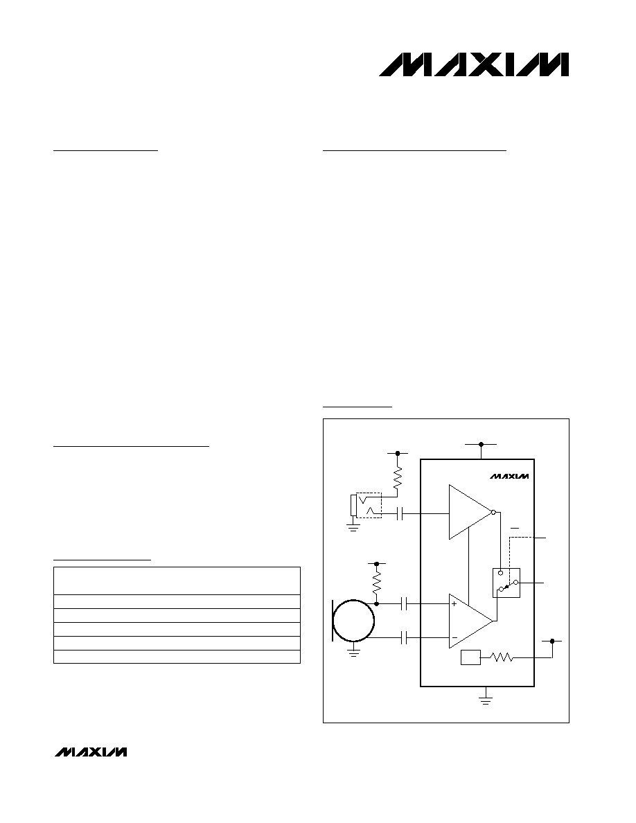
BIAS
BIAS
AUX_IN
8
IN-
IN+
6
5
4
V
CC
2.4V TO 5.5V
MAX4060
INT/AUX 1
OUT 2
GND
7
BIAS
3
V
BIAS
x10
BIAS
x10
Typical Operating Circuit
Ordering Information
19-2408; Rev 1; 1/03
For pricing, delivery, and ordering information, please contact Maxim/Dallas Direct! at
1-888-629-4642, or visit Maxim's website at www.maxim-ic.com.
Pin Configurations and Selector Guide appear at end of
data sheet.
Rail-to-Rail is a registered trademark of Nippon Motorola, Ltd.
*EP = Exposed paddle.
Notebook Audio
Systems
Tablet PCs
PDA Audio Systems
USB Audio Peripherals
AES-42-Compliant
Microphones
Signal Conditioning
PART
TEMP
RANGE
PIN-
PACKAGE
TOP
MARK
MAX4060ETA
-40°C to +85°C
8 Thin QFN-EP*
ABY
MAX4060EUA
-40°C to +85°C
8 µMAX
--
MAX4061ETA
-40°C to +85°C
8 Thin QFN-EP*
ABZ
MAX4061EUA
-40°C to +85°C
8 µMAX
--
MAX4062EUB
-40°C to +85°C
10 µMAX
--
MAX4060/MAX4061/MAX4062
Differential Microphone Preamplifiers with
Internal Bias and Complete Shutdown
2
_______________________________________________________________________________________
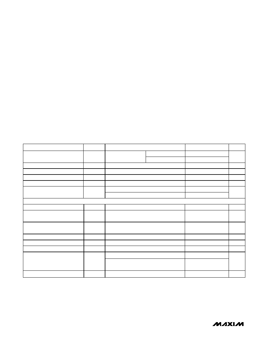
ABSOLUTE MAXIMUM RATINGS
ELECTRICAL CHARACTERISTICS
(V
CC
= 3V for MAX4061/MAX4062, V
CC
= 5V for MAX4060, GND = 0V, SHDN = V
CC
, INT/AUX = 0V, R
G
= 11.11k
,
R
L
= 100k
to 1.5V, R
BIAS
=
, T
A
= T
MIN
to T
MAX
, unless otherwise noted. Typical values are at T
A
= +25°C.) (Notes 1, 2)
Stresses beyond those listed under "Absolute Maximum Ratings" may cause permanent damage to the device. These are stress ratings only, and functional
operation of the device at these or any other conditions beyond those indicated in the operational sections of the specifications is not implied. Exposure to
absolute maximum rating conditions for extended periods may affect device reliability.
Supply Voltage (V
CC
to GND). .................................-0.3V to +6V
Any Other Pin to GND ................................-0.3V to (V
CC
+ 0.3V)
Duration of Short Circuit to GND or V
CC
....................Continuous
Continuous Input Current (any pin) ................................ ±10mA
Continuous Power Dissipation (T
A
= +70°C)
8-Pin Thin QFN (derate 4.7mW/°C above +70°C) ......379mW
8-Pin µMAX (derate 4.1mW/°C above +70°C) ............330mW
10-Pin µMAX (derate 5.6mW/°C above +70°C) .........444mW
Operating Temperature Range ...........................-40°C to +85°C
Junction Temperature ......................................................+150°C
Storage Temperature Range .............................-65°C to +150°C
Lead Temperature (soldering, 10s) .................................+300°C
PARAMETER
SYMBOL
CONDITIONS
MIN
TYP
MAX
UNITS
MAX4061/MAX4062
2.4
5.5
Supply Voltage Range
V
CC
Inferred from
PSRR test
MAX4060
4.5
5.5
V
Supply Current
I
CC
0.75
1.2
mA
Output Common-Mode Voltage
V
OCM
1.25
1.5
1.75
V
Slew Rate
SR
A
V
= 10V/V
±1
V/µs
Supply Current in Shutdown
I
SHDN
V
SHDN
= 0V, MAX4061
0.001
1
µA
To GND
30
Output Short-Circuit Current
I
SC
To V
CC
30
mA
DIFFERENTIAL INPUT (INT/AUX = 0V for MAX4060/MAX4062, default for MAX4061)
Input Offset Voltage
V
OS
±0.1
±5
mV
Common-Mode Input Voltage
Range
V
CM
1
2
V
Maximum Differential Input
Voltage
V
DIFFMAX
A
V
= 1V/V, MAX4061/MAX4062
1
V
Small-Signal Bandwidth
BW
-3dB
600
kHz
Input Resistance
R
IN
Either differential input
100
k
Input Resistance Match
R
MATCH
1
%
A
V
= 10V/V, f = 1kHz
100
Input Noise-Voltage Density
e
n
A
V
= 100V/V, f = 1kHz, MAX4061/MAX4062
only
20
nV/
Hz
RMS Output Noise Voltage
V
NRMS
A
V
= 10V/V, BW = 22Hz to 22kHz
125
µV
RMS
MAX4060/MAX4061/MAX4062
Differential Microphone Preamplifiers with
Internal Bias and Complete Shutdown
_______________________________________________________________________________________
3
ELECTRICAL CHARACTERISTICS (continued)
(V
CC
= 3V for MAX4061/MAX4062, V
CC
= 5V for MAX4060, GND = 0V, SHDN = V
CC
, INT/AUX = 0V, R
G
= 11.11k
,
R
L
= 100k
to 1.5V, R
BIAS
=
, T
A
= T
MIN
to T
MAX
, unless otherwise noted. Typical values are at T
A
= +25°C.) (Notes 1, 2)
PARAMETER
SYMBOL
CONDITIONS
MIN
TYP
MAX
UNITS
Total Harmonic Distortion
Plus Noise
THD+N
A
V
= 10V/V, f = 1kHz, V
OUT
= 0.7V
RMS
,
BW = 22Hz to 22kHz
0.04
%
RG = open
1
1.13
1.3
RG = 11.11k
9.6
10
10.4
1V < V
CM
< 2V,
VOUT = 0.7V
RMS
,
MAX4061/MAX4062
RG = 1.01k
96
100
104
Differential Gain
A
VDIFF
1V < V
CM
< 2V, V
OUT
= 0.7V
RMS
, MAX4060
9.6
10.0
10.4
V/V
Common-Mode Rejection Ratio
CMRR
V
CM
= 500mV
P-P
, f = 1kHz
70
dB
T
A
= +25°C
72
89
T
A
= T
MIN
to TMAX
60
Power-Supply Rejection Ratio
PSRR
V
CC
= 5V
±100mV, f = 1kHz
86
dB
AUXILIARY INPUT (MAX4060/MAX4062, INT/AUX = V
CC
)
Small-Signal Bandwidth
BW
-3dB
200
kHz
Input Resistance
R
IN
100
k
Input Noise-Voltage Density
en
f = 1kHz
45
nV/
Hz
RMS Output Noise Voltage
V
NRMS
BW = 22Hz to 22kHz
385
µV
RMS
Total Harmonic Distortion
Plus Noise
THD+N
f = 1kHz, BW = 22Hz to 22kHz
0.05
%
T
A
= +25°C
65
90
Power-Supply Rejection Ratio
PSRR
T
A
= T
MIN
- T
MAX
50
dB
Voltage Gain
A
VAUX
V
OUT
= 0.7V
RMS
-10.7
-10
-9.3
V/V
BIAS OUTPUT (MAX4060/MAX4062)
I
BIAS
= 0.8mA to GND, MAX4060
2
2.2
Output Voltage
V
OUT
I
BIAS
= 0.5mA to GND, MAX4062
2
2.2
V
I
BIAS
= 0.8mA to GND, MAX4060
2
2.5
k
Output Resistance
R
OUT
I
BIAS
= 0.5mA to GND, MAX4062
22
40
I
BIAS
= 0.8mA to GND, BW = 22Hz to
22kHz, MAX4060
50
Output Noise Voltage
V
NRMS
I
BIAS
= 0.5mA to GND, BW = 22Hz to
22kHz, MAX4062
20
µV
RMS
MAX4060/MAX4061/MAX4062
Differential Microphone Preamplifiers with
Internal Bias and Complete Shutdown
4
_______________________________________________________________________________________
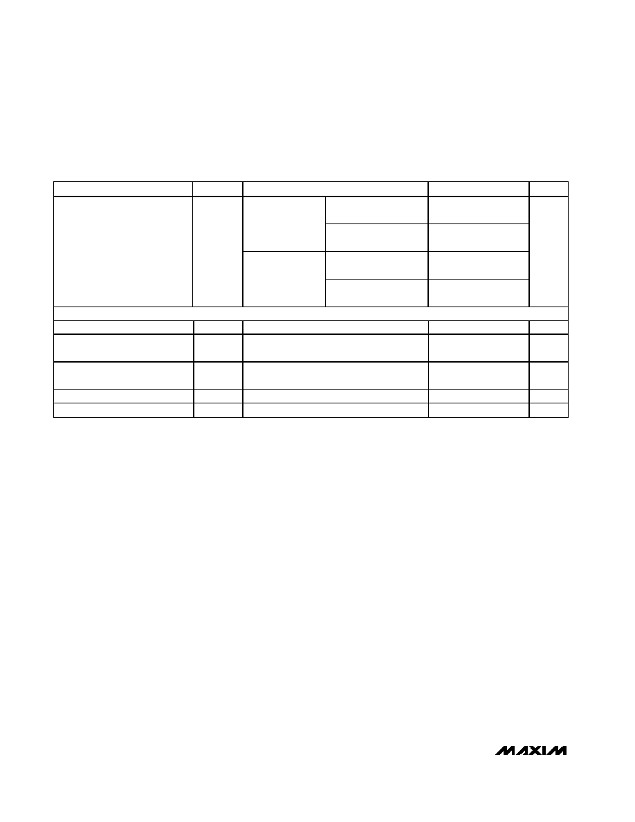
ELECTRICAL CHARACTERISTICS (continued)
(V
CC
= 3V for MAX4061/MAX4062, V
CC
= 5V for MAX4060, GND = 0V, SHDN = V
CC
, INT/AUX = 0V, R
G
= 11.11k
,
R
L
= 100k
to 1.5V, R
BIAS
=
, T
A
= T
MIN
to T
MAX
, unless otherwise noted. Typical values are at T
A
= +25°C.) (Notes 1, 2)
PARAMETER
SYMBOL
CONDITIONS
MIN
TYP
MAX
UNITS
I
BIAS
= 0.8mA to GND,
V
CC
= 4.5V to 5.5V
50
80
MAX4060
I
BIAS
= 0.8mA, V
CC
= 5V
+ 100mV
P-P
, f = 1kHz
70
I
BIAS
= 0.5mA to GND,
V
CC
= 2.4V to 5.5V
50
74
Power-Supply Rejection Ratio
PSRR
M AX 4062
I
BIAS
= 0.5mA, V
CC
= 3V
+ 100mV
P-P
, f = 1kHz
71
dB
DIGITAL INPUTS ( SHD N for M AX 4061 and INT/AU X for M AX 4060/M AX 4062)
Input Leakage Current
I
IN
V
IN
= 0V or V
CC
±1
µA
Input Voltage High
V
INH
0.7
V
CC
V
Input Voltage Low
V
INL
0.3
V
CC
V
Shutdown Enable Time
t
ON
MAX4061
10
µs
Shutdown Disable Time
t
OFF
MAX4061
10
µs
Note 1: All specifications are 100% tested at T
A
= +25
°C. Specification limits over temperature (T
A
= T
MIN
to T
MAX
) are guaranteed
by design, not production tested.
Note 2: MAX4062 requires a 1µF capacitor from BIAS to ground.
MAX4060/MAX4061/MAX4062
Differential Microphone Preamplifiers with
Internal Bias and Complete Shutdown
_______________________________________________________________________________________
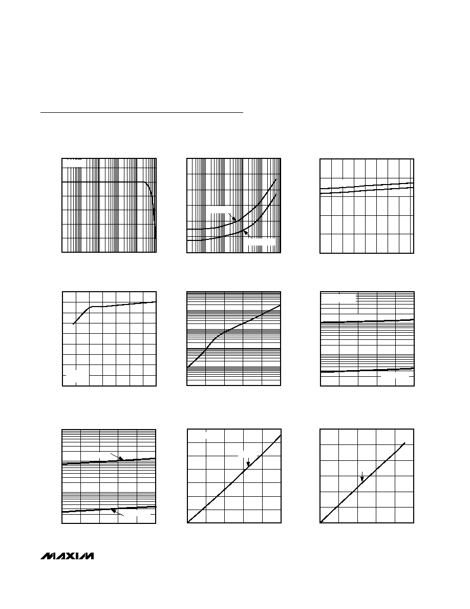
5
MAX4060 toc01
FREQUENCY (Hz)
GAIN (dB)
100k
10k
1k
100
-12
-9
-6
-3
0
3
-15
10
1M
GAIN vs. FREQUENCY
(NO LOAD)
V
CC
= 5V
MAX4060 toc02
FREQUENCY (Hz)
PSRR (dB)
100k
10k
1k
100
-100
-80
-60
-40
-20
0
-120
10
1M
POWER-SUPPLY REJECTION RATIO
vs. FREQUENCY (DIFF INPUT)
A
V
= 100V/V
A
V
= 10V/V
SUPPLY CURRENT vs. TEMPERATURE
MAX4060 toc03
TEMPERATURE (
°C)
SUPPLY CURRENT (mA)
80
65
50
35
20
5
-10
-25
0.2
0.4
0.6
0.8
1.0
0
-40
V
CC
= 3V
V
CC
= 5V
SUPPLY CURRENT vs. SUPPLY VOLTAGE
MAX4060 toc04
SUPPLY VOLTAGE (V)
SUPPLY CURRENT (mA)
5.0
4.5
3.5
4.0
3.0
2.5
0.1
0.2
0.3
0.4
0.5
0.6
0.7
0.8
0.9
0
2.0
5.5
A
V
= 10V/V
NO LOAD
SHUTDOWN SUPPLY CURRENT
vs. TEMPERATURE
MAX4060 toc05
TEMPERATURE (
°C)
SHUTDOWN SUPPLY CURRENT (nA)
60
35
10
-15
0.01
0.1
1
10
100
0.001
-40
85
V
OH
vs. TEMPERATURE
MAX4060 toc06
TEMPERATURE (
°C)
V
OH
(mV)
60
35
10
-15
10
100
1000
1
-40
85
I
LOAD
= 2.5mA
I
LOAD
= 50
µA
V
OH
= V
CC
- V
OUT
V
OL
vs. TEMPERATURE
MAX4060 toc07
TEMPERATURE (
°C)
V
OL
(mV)
60
35
10
-15
10
100
1000
1
-40
85
I
LOAD
= 2.5mA
I
LOAD
= 50
µA
V
OH
vs. LOAD CURRENT
MAX4060 toc08
LOAD CURRENT (mA)
V
OH
(mV)
4
3
2
1
25
50
75
100
125
150
175
0
0
5
V
OH
= V
CC
- V
OUT
V
CC
= 3V
V
OL
vs. LOAD CURRENT
MAX4060 toc09
LOAD CURRENT (mA)
V
OL
(mV)
4
3
2
1
50
100
150
200
250
300
0
0
5
V
CC
= 3V
Typical Operating Characteristics
(V
CC
= 3V (MAX4061/MAX4062), V
CC
= 5V for MAX4060, A
V
= 10V/V, R
L
100k to 1.5V, SHDN = V
CC
(MAX4061 only),
T
A
= +25°C, unless otherwise noted.)