 | –≠–ª–µ–∫—Ç—Ä–æ–Ω–Ω—ã–π –∫–æ–º–ø–æ–Ω–µ–Ω—Ç: MAX4146 | –°–∫–∞—á–∞—Ç—å:  PDF PDF  ZIP ZIP |
________________General Description
The MAX4144/MAX4145/MAX4146 differential line
receivers offer unparalleled high-speed, low-distortion
performance. Using a three op-amp instrumentation
amplifier architecture, these ICs have fully symmetrical
differential inputs and a single-ended output. They
operate from ±5V power supplies and are capable of
driving a 150
load to ±3.7V. The MAX4144 has an
internally set closed-loop gain of +2V/V. The MAX4145
is optimized for gains from +1V/V to +10V/V, while the
MAX4146 is optimized for gains from +10V/V to
+100V/V. The MAX4145/MAX4146 require a single
external resistor to set the closed-loop gain.
These amplifiers use laser-trimmed, matched thin-film
resistors to deliver a common-mode rejection (CMR) of
up to 90dB at 10MHz. Using current-feedback tech-
niques, the MAX4144 achieves a 130MHz bandwidth
and a 1000V/µs slew rate. The MAX4145 achieves a
bandwidth of 180MHz and a slew rate of 600V/µs while
operating with a closed-loop gain of +1V/V, and the
MAX4146 features a bandwidth of 70MHz and a slew
rate of 800V/µs with a gain of +10V/V. Excellent differ-
ential gain/phase and noise specifications make these
amplifiers ideal for a wide variety of video and RF
signal-processing applications.
For a complete differential transmission link, use the
MAX4144/MAX4145/MAX4146 with the MAX4147 differ-
ential line driver (see the MAX4147 data sheet for more
information).
________________________Applications
Differential to Single-Ended Conversion
Twisted-Pair to Coaxial Converter
High-Speed Instrumentation Amplifier
Data Acquisition
Medical Instrumentation
High-Speed Differential Line Receiver
____________________________Features
MAX4144:
o
+2V/V Internally Fixed Gain
o
130MHz Bandwidth
o
1000V/µs Slew Rate
o
70dB CMR at 10MHz
o
-90dBc SFDR (f = 10kHz)
o
Low Differential Gain/Phase: 0.03%/0.03∞
o
800µA Shutdown
MAX4145:
o
External Gain Selection from +1V/V to +10V/V
o
180MHz Bandwidth
o
90MHz 0.1dB Gain Flatness
o
600V/µs Slew Rate
o
75dB CMR at 10MHz
o
-92dBc SFDR (f = 10kHz)
o
Very Low Noise: 3.8nV/
Hz
(G = +10V/V)
o
800µA Shutdown
MAX4146:
o
External Gain Selection from +10V/V to +100V/V
o
70MHz Bandwidth (A
V
= +10V/V)
o
800V/µs Slew Rate
o
90dB CMR at 10MHz
o
-82dBc SFDR (f = 10kHz)
o
Very Low Noise: 3.45nV/
Hz
(G = +100V/V)
o
800µA Shutdown
MAX4144/MAX4145/MAX4146
High-Speed, Low-Distortion,
Differential Line Receivers
________________________________________________________________
Maxim Integrated Products
1
19-1147; Rev 1; 1/98
PART
MAX4144
ESD
MAX4146
ESD
-40∞C to +85∞C
-40∞C to +85∞C
TEMP. RANGE
PIN-PACKAGE
14 SO
14 SO
EVALUATION KIT
AVAILABLE
_______________Ordering Information
For free samples & the latest literature: http://www.maxim-ic.com, or phone 1-800-998-8800
For small orders, phone 408-737-7600 ext. 3468.
Pin Configurations appear at end of data sheet.
Typical Application Circuit appears at end of data sheet.
MAX4145
ESD
-40∞C to +85∞C
14 SO
MAX4144EEE
-40∞C to +85∞C
16 QSOP
MAX4145EEE
-40∞C to +85∞C
16 QSOP
MAX4146EEE
-40∞C to +85∞C
16 QSOP
MAX4144/MAX4145/MAX4146
High-Speed, Low-Distortion,
Differential Line Receivers
2
_______________________________________________________________________________________
ABSOLUTE MAXIMUM RATINGS
DC ELECTRICAL CHARACTERISTICS
(V
CC
= +5V, V
EE
= -5V, SHDN = 0V, R
L
=
, T
A
= T
MIN
to T
MAX
, unless otherwise noted. Typical values are at T
A
= +25∞C.)
Stresses beyond those listed under "Absolute Maximum Ratings" may cause permanent damage to the device. These are stress ratings only, and functional
operation of the device at these or any other conditions beyond those indicated in the operational sections of the specifications is not implied. Exposure to
absolute maximum rating conditions for extended periods may affect device reliability.
Supply Voltage (V
CC
to V
EE
) ..................................................12V
Voltage on IN_, SHDN, REF, OUT,
SENSE, RG_.................................(V
EE
- 0.3V) to (V
CC
+ 0.3V)
Short-Circuit Duration to Ground ........................................10sec
Input Current (IN_, RG_)...................................................±10mA
Output Current................................................................±120mA
Continuous Power Dissipation (T
A
= +70∞C)
14-Pin SO (derate 8.33mW/∞C above +70∞C)..............667mW
16-Pin QSOP (derate 8.33mW/∞C above +70∞C).........667mW
Operating Temperature Range ...........................-40∞C to +85∞C
Storage Temperature Range .............................-65∞C to +150∞C
Lead Temperature (soldering, 10sec) .............................+300∞C
PARAMETER
SYMBOL
MIN
TYP
MAX
UNITS
Differential Input Resistance
R
IN
1
M
Input Capacitance
C
IN
1
pF
Input Offset Current
I
OS
0.1
2.5
µA
Differential Input Voltage Range
-1.55
1.55
-2.8/G
2.8/G
V
-3.1/G
3.1/G
Common-Mode Input Voltage
Range
V
CM
-2.8
2.8
V
Input Offset Voltage Drift
Operating Supply Voltage
±4.5
±5.5
V
TC
VOS
5
µV/∞C
Input Bias Current
I
B
9
20
µA
2
Gain
A
V
1 + (1.4k
/R
G
)
V/V
10 + (14k
/R
G
)
0.02
2
0.5
2
Gain Error
1.5
5
%
0.5
2
1.5
5
20
Gain Drift
5 + 15G
ppm/∞C
14 + 0.9G
Common-Mode Rejection
CMR
60
80
dB
Power-Supply Rejection
PSR
70
85
dB
-1V
V
OUT
+1V,
R
L
= 150
V
IN
= 0V
R
L
= 150
Guaranteed by CMR test
-1V
V
OUT
+1V,
R
L
= 150
V
IN
= 0V
-1V
V
OUT
+1V,
R
L
= 150
V
IN
= 0V
V
S
= ±4.5V to ±5.5V
MAX4144
MAX4145
MAX4146
V
CM
= ±2.8V
CONDITIONS
MAX4144
MAX4145
MAX4144
MAX4145
MAX4146
MAX4146
A
V
= 1V/V
A
V
= 10V/V
A
V
= 10V/V
Guaranteed by PSR test
A
V
= 100V/V
MAX4144
MAX4145
MAX4146
Quiescent Supply Current
11
16
mA
Shutdown Supply Current
I
SHDN
0.8
2
mA
Shutdown Output Impedance
1.4
1.4
k
2
±3.6
Output Voltage Swing
V
OUT
±3.1
±3.7
V
±3.4
±3.8
R
L
= 100
R
L
= 150
V
SHDN
2V
V
SHDN
2V
R
L
=
MAX4144
MAX4145
MAX4146
A
V
= 2V/V
Input Offset Voltage
V
OS
0.6
8
mV
V
IN
= 0V

MAX4144/MAX4145/MAX4146
High-Speed, Low-Distortion,
Differential Line Receivers
_______________________________________________________________________________________
3
AC ELECTRICAL CHARACTERISTICS
(V
CC
= +5V, V
EE
= -5V, SHDN = 0V, R
L
= 150
, T
A
= T
MIN
to T
MAX
, unless otherwise noted. Typical values are at T
A
= +25∞C.)
DC ELECTRICAL CHARACTERISTICS (continued)
(V
CC
= +5V, V
EE
= -5V, SHDN = 0V, R
L
=
, T
A
= T
MIN
to T
MAX
, unless otherwise noted. Typical values are at T
A
= +25∞C.)
PARAMETER
SYMBOL
MIN
TYP
MAX
UNITS
30
70
-3dB Bandwidth
BW
(-3dB)
180
MHz
130
110
180
Full-Power Bandwidth
FPBW
70
MHz
30
30
0.1dB Bandwidth
BW
(0.1dB)
90
MHz
50
1.7
i
n
pA/
Hz
1000
Slew Rate
SR
600
V/µs
800
23
20
17
Settling Time to 0.1%
t
S
36
ns
CONDITIONS
V
OUT
0.1V
RMS
V
OUT
0.1V
RMS
V
OUT
=
2Vp-p
f = 1MHz
-2V
V
OUT
+2V
-2V
V
OUT
+2V
MAX4144
MAX4145
MAX4146
MAX4145
MAX4144
MAX4144
MAX4145
MAX4146
MAX4146
to 0.1%
A
V
= 100V/V
A
V
= 10V/V
A
V
= 10V/V
A
V
= 100V/V
MAX4144
MAX4145
MAX4146
MAX4144
MAX4145
MAX4146
MAX4144
38
40
Enable Time from Shutdown
45
ns
Disable Time to Shutdown
40
µs
0.03
Differential Gain (Note 1)
DG
0.01
%
0.12
f = 3.58MHz
to 0.01%
MAX4145
MAX4145
MAX4146
MAX4146
MAX4144
PARAMETER
SYMBOL
MIN
TYP
MAX
UNITS
CONDITIONS
Output Current Drive
I
OUT
80
100
mA
60
SHDN High Threshold
V
IH
2
V
SHDN Low Threshold
V
IL
0.8
V
SHDN Input Bias Current
I
SHDN
75
150
µA
0.06
2
V
OUT
= ±1.7V
V
SHDN
0.8V
V
SHDN
2V
0∞C
T
A
+85∞C
-40∞C
T
A
0∞C
A
V
= 2V/V
A
V
= 1V/V
A
V
= 2V/V
A
V
= 1V/V
A
V
= 2V/V
A
V
= 1V/V
A
V
= 10V/V
MAX4144
12
Input Voltage Noise Density
e
n
1.8 + (20/G)
nV/
Hz
2.1 + (135/G)
f = 1MHz
MAX4145
MAX4146
70
Common-Mode Rejection
CMR
75
dB
90
f = 10MHz
MAX4144
MAX4145
MAX4146
Input Current Noise Density

MAX4144/MAX4145/MAX4146
High-Speed, Low-Distortion,
Differential Line Receivers
4
_______________________________________________________________________________________
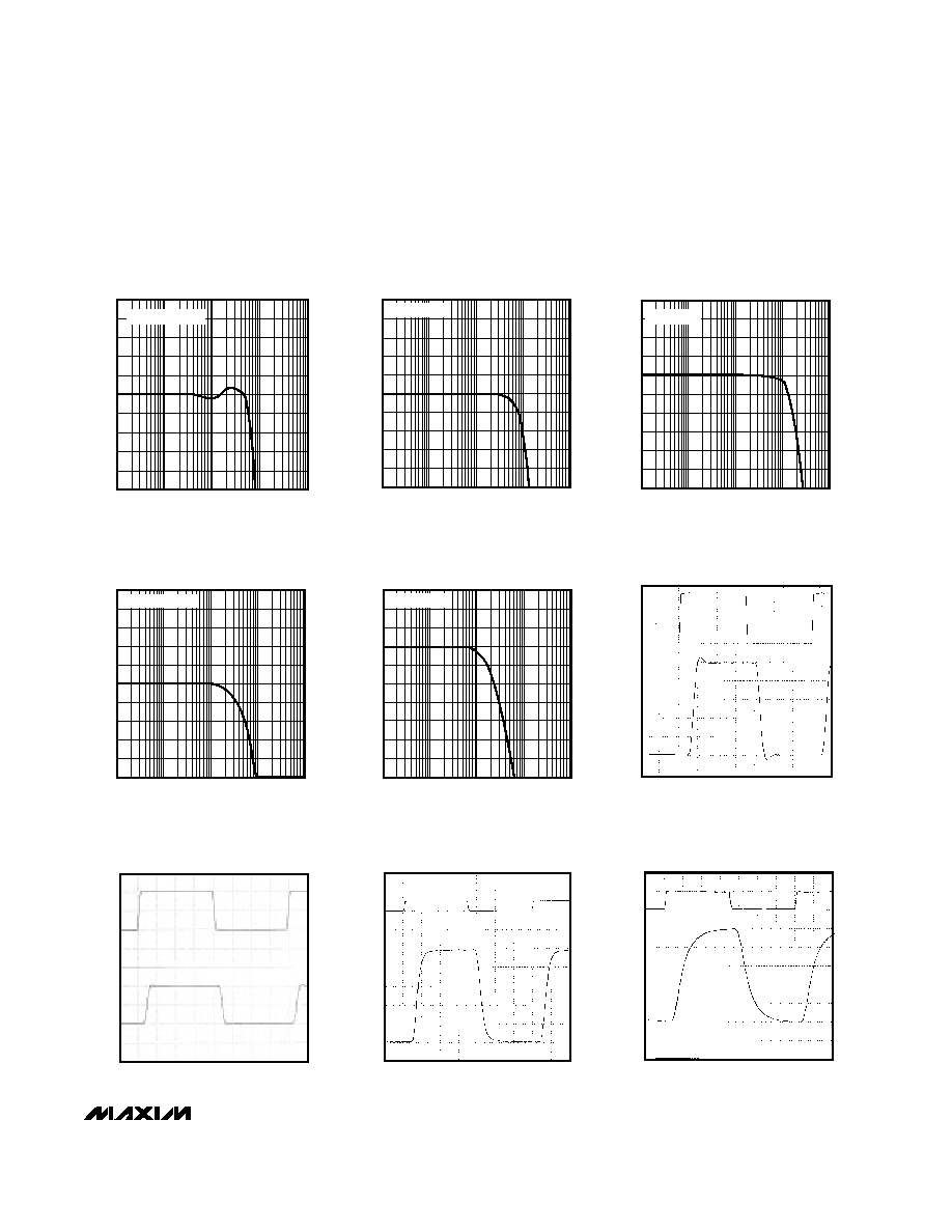
__________________________________________Typical Operating Characteristics
(V
CC
= +5V, V
EE
= -5V, SHDN = 0V, R
L
= 150
, T
A
= +25∞C, unless otherwise noted.)
-5
-4
-3
-2
-1
0
1
2
3
4
5
100k
1M
10M
100M
1G
MAX4146
SMALL-SIGNAL GAIN
vs. FREQUENCY (A
V
= +100)
MAX4144/4146-04
FREQUENCY (Hz)
NORMALIZED
GAIN (dB)
V
OUT
= 100mV
RMS
0.5
0.4
-0.5
100k
1M
10M
100M
1G
MAX4144
0.1dB GAIN FLATNESS vs.
FREQUENCY (A
V
= +2)
0
-0.1
-0.2
-0.3
-0.4
MAX444/46 TOC05
FREQUENCY (Hz)
NORMALIZED GAIN (dB)
0.1
0.2
0.3
V
OUT
= 100mV
RMS
5
-5
100k
1M
10M
100M
1G
MAX4144
SMALL-SIGNAL GAIN
vs. FREQUENCY (A
V
= +2)
-3
MAX4144/6 TOC-01
FREQUENCY (Hz)
NORMALIZED GAIN (dB)
-1
1
3
4
-4
-2
0
2
V
OUT
= 100mV
RMS
4
-6
100k
1M
10M
100M
1G
MAX4145
SMALL-SIGNAL GAIN
vs. FREQUENCY (A
V
= +1)
-4
MAX4144/6 TOC-02
FREQUENCY (Hz)
GAIN (dB)
-2
0
2
3
-5
-3
-1
1
V
OUT
= 100mV
RMS
5
-5
100k
1M
10M
100M
1G
MAX4146
SMALL-SIGNAL GAIN
vs. FREQUENCY (A
V
= +10)
-3
MAX4144/6 TOC-03
FREQUENCY (Hz)
NORMALIZED GAIN (dB)
-1
1
3
4
-4
-2
0
2
V
OUT
= 100mV
RMS
0.5
0.4
-0.5
100k
1M
10M
100M
1G
MAX4145
0.1dB GAIN FLATNESS vs.
FREQUENCY (A
V
= +1)
0
-0.1
-0.2
-0.3
-0.4
MAX4144/46 TOC06a
FREQUENCY (Hz)
NORMAILIZED GAIN (dB)
0.1
0.2
0.3
V
OUT
= 100mV
RMS
AC ELECTRICAL CHARACTERISTICS (continued)
(V
CC
= +5V, V
EE
= -5V, SHDN = 0V, R
L
= 150
, T
A
= T
MIN
to T
MAX
, unless otherwise noted. Typical values are at T
A
= +25∞C.)
PARAMETER
SYMBOL
MIN
TYP
MAX
UNITS
CONDITIONS
0.03
0.06
Differential Phase (Note 1)
DP
0.07
Degrees
-66
-67
-48
f = 3.58MHz
f = 5MHz,
V
OUT
= 2Vp-p
MAX4144
MAX4145
MAX4146
Note 1:
Differential gain and phase are tested using a modulated ramp, 100 IRE (0.714V).
-90
-92
Spurious-Free Dynamic Range
SFDR
-82
dBc
f = 10kHz,
V
OUT
= 2Vp-p
MAX4144
MAX4145
MAX4146
A
V
= 2V/V
A
V
= 1V/V
A
V
= 10V/V
A
V
= 2V/V
A
V
= 1V/V
A
V
= 10V/V
MAX4144
MAX4145
MAX4146
MAX4144/MAX4145/MAX4146
High-Speed, Low-Distortion,
Differential Line Receivers
_______________________________________________________________________________________
5
-7
-6
-5
-4
-3
-2
-1
0
1
2
3
100k
1M
10M
100M
1G
MAX4146
LARGE-SIGNAL GAIN
vs. FREQUENCY (A
V
= +100)
MAX4144/4146-10
FREQUENCY (Hz)
NORMALIZED GAIN (dB)
V
OUT
= 2Vp-p
TIME (10ns/div)
MAX4144
SMALL-SIGNAL
PULSE RESPONSE (A
V
= +2)
IN
OUT
GND
GND
VOLTAGE (20mV/div)
TOC-11
GND
TIME (10ns/div)
GND
MAX4144/4146 TOC12
IN
OUT
VOLTAGE (50mV/div)
MAX4145
SMALL-SIGNAL
PULSE RESPONSE (A
V
= +1)
TIME (10ns/div)
MAX4146
SMALL-SIGNAL
PULSE RESPONSE (A
V
= +10)
IN
OUT
GND
GND
VOLTAGE (20mV/div)
TOC-13
TIME (10ns/div)
MAX4146
SMALL-SIGNAL
PULSE RESPONSE (A
V
= +100)
GND
GND
VOLTAGE
IN
OUT
1mV/div
20mV/div
TOC-14
_____________________________Typical Operating Characteristics (continued)
(V
CC
= +5V, V
EE
= -5V, SHDN = 0V, R
L
= 150
, T
A
= +25∞C, unless otherwise noted.)
-5
-4
-3
-2
-1
0
1
2
3
4
5
100k
1M
10M
100M
1G
MAX4144
LARGE-SIGNAL GAIN
vs. FREQUENCY (A
V
= +2)
MAX4144/4146-07
FREQUENCY (Hz)
NORMALIZED GAIN (dB)
V
OUT
= 2Vp-p
4
3
-6
100k
1M
10M
100M
1G
MAX4145
LARGE-SIGNAL GAIN
vs. FREQUENCY (A
V
= +1)
-1
-2
-3
-4
-5
MAX4144/46 TOC-8
FREQUENCY (Hz)
NORMALIZED GAIN (dB)
0
1
2
V
OUT
= 2Vp-p
5
-5
100k
1M
10M
100M
1G
MAX4146
SMALL-SIGNAL GAIN
vs. FREQUENCY (A
V
= +10)
-3
MAX4144/6 TOC-09
FREQUENCY (Hz)
NORMALIZED GAIN (dB)
-1
1
3
4
-4
-2
0
2
V
OUT
= 100mV
RMS
0.5
0.4
-0.5
100k
1M
10M
100M
1G
MAX4146
0.1dB GAIN FLATNESS vs.
FREQUENCY (A
V
= +10)
0
-0.1
-0.2
-0.3
-0.4
MAX4144/46 TOC06
FREQUENCY (Hz)
NORMALIZED GAIN (dB)
0.1
0.2
0.3
V
OUT
= 100mV
RMS