 | –≠–ª–µ–∫—Ç—Ä–æ–Ω–Ω—ã–π –∫–æ–º–ø–æ–Ω–µ–Ω—Ç: MAX4361 | –°–∫–∞—á–∞—Ç—å:  PDF PDF  ZIP ZIP |

General Description
The MAX4361/MAX4362/MAX4363 are a family of high-
performance ADSL drivers and drivers/receivers ideal
for the upstream transmit path and the downstream
receive path of customer premise equipment. These
devices operate from a single 5V supply and deliver up
to 12.5dBm average line power for DMT modulated sig-
nals, meeting the requirements of full-rate ADSL.
Spurious-free dynamic range (SFDR) at full output
power is typically -75dBC at 100kHz.
The MAX4361 is a differential IN/differential OUT driver
with a fixed gain of 3.1V/V. The MAX4362 is a dual
amplifier with shutdown intended for use as a differen-
tial IN/differential OUT driver with gain set with external
resistors. The MAX4363 is a quad amplifier with shut-
down intended for use as a differential IN/differential
OUT driver/receiver combination with gain set with
external resistors.
The MAX4361 is offered in a space-saving 8-pin µMAX
package.
Applications
ADSL Line Interface
HDSL Line Driver
Features
o Low-Noise Driver
4.8nV/
Hz Voltage-Noise Density
1.5pA/
Hz Current-Noise Density
o Full-Rate ADSL ATU-R Line Drivers and Receivers
o Single 5V Supply
o -75dBc SFDR at Full Output Power at 100kHz
o -95dB Driver-to-Receiver Crosstalk (MAX4363)
o +12.5dBm Average Line Power (DMT)
o 280mA (min) Peak Output Current
o Rail-to-Rail
Æ
Output Swing
o Thermal and Short-Circuit Protection
MAX4361/MAX4362/MAX4363
ADSL Drivers/Receivers for Customer Premise
Equipment
________________________________________________________________ Maxim Integrated Products
1
1
2
3
4
5
10
9
8
7
6
GND
T1OUT
V+
T2OUT
T2IN-
SHDN
T1IN-
T1IN+
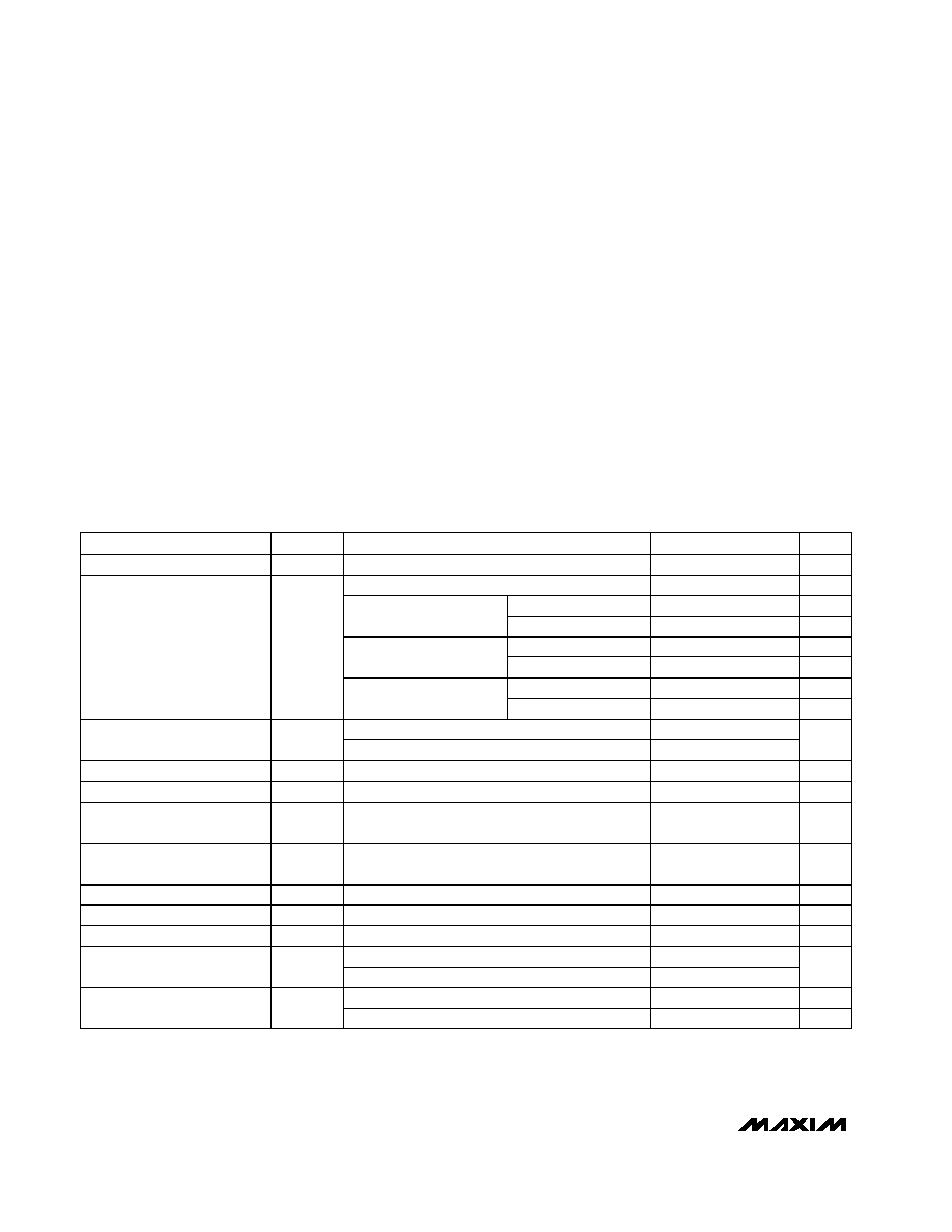
µMAX
GND
T2IN+
2
7 V+
IN+
1
8 OUT+
GND
µMAX/SO
TOP VIEW
V+
IN- 3
6
OUT-
GND 4
5
MAX4361
MAX4362
MAX4362
MAX4363
11
4
V+
SHDN
12
3
T1OUT
T1IN-
13
2
GND
T1IN+
14
1
N.C.
N.C.
8
7
N.C.
N.C.
9
6
GND
T2IN+
10
5
T2OUT
T2IN-
SO
20
19
18
17
16
15
14
13
1
2
3
4
5
6
7
8
GND (TX)
T1OUT
V+ (TX)
T2OUT
T2IN-
SHDN
T1IN-
T1IN+
GND (TX)
N.C.
V+ (RX)
GND (RX)
R1IN-
R1IN+
GND
T2IN+
12
11
9
10
R1OUT
R2OUT
R2IN+
R2IN-
SO/TSSOP
Pin Configurations
Ordering Information
19-2299; Rev 0; 1/02
For pricing, delivery, and ordering information, please contact Maxim/Dallas Direct! at
1-888-629-4642, or visit Maxim's website at www.maxim-ic.com.
PART
TEMP RANGE
PIN-PACKAGE
MAX4361EUA
-40∞C to +85∞C
8 µMAX
MAX4361ESA
-40∞C to +85∞C
8 SO
MAX4362EUB
-40∞C to +85∞C
10 µMAX
MAX4362ESD
-40∞C to +85∞C
14 SO
MAX4363EUP
-40∞C to +85∞C
20 TSSOP
MAX4363ESP
-40∞C to +85∞C
20 SO
Rail-to-Rail is a registered trademark of Nippon Motorola, Ltd.
MAX4361/MAX4362/MAX4363
ADSL Drivers/Receivers for Customer Premise
Equipment
2
_______________________________________________________________________________________
ABSOLUTE MAXIMUM RATINGS
ELECTRICAL CHARACTERISTICS--Driver
(V+ = 5V, GND = 0, V
CM
= 2.5V, R
L
= 12.5
, SHDN = 0, T
A
= T
MIN
to T
MAX
, unless otherwise noted. Typical values specified at
T
A
= +25∞C.)
Stresses beyond those listed under "Absolute Maximum Ratings" may cause permanent damage to the device. These are stress ratings only, and functional
operation of the device at these or any other conditions beyond those indicated in the operational sections of the specifications is not implied. Exposure to
absolute maximum rating conditions for extended periods may affect device reliability.
Supply Voltage (V+ to GND) ....................................-0.3V to +6V
Analog Input Voltage .......................(GND - 0.3V) to (V+ + 0.3V)
SHDN Input Voltage.........................(GND - 0.3V) to (V+ + 0.3V)
Output Short-Circuit Duration .................................................10s
Driver Output Current...............................................................1A
Receiver Output Current ...................................................150mA
Continuous Power Dissipation (T
A
= +70∞C)
8-Pin µMAX (derate 4.5mW/∞C above +70∞C) ..............362mW
10-Pin µMAX (derate 5.6mW/∞C above +70∞C) ............444mW
8-Pin SO (derate 5.88mW/∞C above +70∞C).................471mW
14-Pin SO (derate 8.33mW/∞C above +70∞C)...............667mW
20-Pin SO (derate 10.0mW/∞C above +70∞C)...............800mW
20-Pin TSSOP (derate 10.9mW/∞C above +70∞C) ........879mW
Operating Temperature Range ...........................-40∞C to +85∞C
Junction Temperature ......................................................+150∞C
Storage Temperature Range .............................-65∞C to +150∞C
Lead Temperature (soldering, 10s) .................................+300∞C
PARAMETER
SYMBOL
CONDITIONS
MIN
TYP
MAX
UNITS
S up p l y V ol tag e Rang e ( N ote 1)
V
CC
4.5
5.5
V
MAX4361, R
L
=
22
33
mA
SHDN = 0
22
33
mA
MAX4362, R
L
=
SHDN = 5V
60
200
µA
SHDN = 0
22
33
mA
MAX4363, measured at
V+ (TX), R
L
=
SHDN = 5V
60
200
µA
SHDN = 0
4
6.5
mA
Supply Current
I
Q
MAX4363, measured at
V+ (RX), R
L
=
SHDN = 5V
70
200
µA
DMT modulation
15.5
Maximum Average Output
Power (Notes 2, 3)
P
OUT
CAP modulation
18
dBm
Gain
G
MAX4361 (0.7V
V
OUT
(V+) - 0.7V)
3.0
3.1
3.2
V/V
Open-Loop Gain
A
VOL
MAX4362/MAX4363 (0.7V
V
OUT
(V+) - 0.7V)
68
81
dB
Second Harmonic Distortion
(Notes 3, 4)
G = 3.1, f = 100kHz, V
OUT(DIFF)
= 7.1V
P-P
-66
-76
dBc
Third Harmonic Distortion
(Notes 3, 4)
G = 3.1, f = 100kHz, V
OUT(DIFF)
= 7.1V
P-P
-68
-79
dBc
Peak Output Current
I
OUT
Inferred from Output Voltage Swing test
280
330
mA
Input Offset Voltage
V
OS
±0.5
±10
mV
Input Bias Current
I
B
1.6
4.5
µA
MAX4361
±30
±600
Input Offset Current
I
OS
MAX4362/MAX4363
±10
±500
nA
MAX4361
25
M
Differential Input Resistance
R
IN(DIFF)
MAX4362/MAX4363
40
k

MAX4361/MAX4362/MAX4363
ADSL Drivers/Receivers for Customer Premise
Equipment
_______________________________________________________________________________________
3
ELECTRICAL CHARACTERISTICS--Driver (continued)
(V+ = 5V, GND = 0, V
CM
= 2.5V, R
L
= 12.5
, SHDN = 0, T
A
= T
MIN
to T
MAX
, unless otherwise noted. Typical values specified at
T
A
= +25∞C.)
PARAMETER
SYMBOL
CONDITIONS
MIN
TYP
MAX
UNITS
Input Common-Mode Voltage
Range
V
CM
Inferred from CMRR test
1.25
4.50
V
MAX4361
60
73
Common-Mode Rejection
Ratio
CMRR
1.25V
V
CM
4.5V
MAX4362/MAX4363
70
85
dB
MAX4361
60
89
Power-Supply Rejection Ratio
PSRR
V+ = 4.5V to 5.5V
MAX4362/MAX4363
60
74
dB
MAX4361
63
AC Power-Supply Rejection
Ratio
PSRR
AC
f = 100kHz
MAX4362/MAX4363
49
dB
Differential Output-Voltage
Swing (Note 4)
V
OU T ( D IF F )
Inferred from Output Voltage Swing test
7.4
8.2
V
P-P
(V+) - V
OH
215
550
R
L
= 100
V
OL
230
550
(V+) - V
OH
400
600
MAX4362/MAX4363
R
L
= 12.5
V
OL
430
650
(V+) - V
OH
400
600
Output-Voltage Swing
(Note 4)
V
OH
,
V
OL
MAX4361, RL = 12.5
,
T
A
= -20∞C to 85∞C
V
OL
430
650
mV
Output Short-Circuit Current
I
SC
±650
mA
MAX4361
0.3
Output Resistance
R
OUT
MAX4362/MAX4363, G = 1
0.001
SHDN Logic Low
V
IL
0.8
V
SHDN Logic High
V
IH
2.0
V
SHDN Input Current
I
IH
, I
IL
SHDN = 0 or SHDN = V+
±10
µA
Shutdown Output Impedance
Z
OUT(SD)
f = 1MHz
1.8
k
MAX4361
40
-3dB Bandwidth
BW
MAX4362/MAX4363, G = 1
60
MHz
Slew Rate
SR
V
OUT(DIFF)
= 7.1V
P-P
step
30
V/µs
MAX4361
115
Settling Time (1%)
t
S
V
OUT(DIFF)
= 7.1V
P-P
step
MAX4362/MAX4363,
G = 3
165
ns
Voltage-Noise Density
e
n
f = 100kHz to 1.1MHz
4.8
nV /
Hz
Current-Noise Density
i
n
f = 100kHz to 1.1MHz
1.5
p A/
Hz
Capacitive-Load Stability
10
nF
Shutdown Delay Time
t
SHDN
400
ns
Enable Delay Time
t
ENABLE
2.8
µs
MAX4361/MAX4362/MAX4363
ADSL Drivers/Receivers for Customer Premise
Equipment
4
_______________________________________________________________________________________
Note 1: Guaranteed by the Power-Supply Rejection Ratio (PSRR) test.
Note 2: Implied by worst-case output-voltage swing (V
OUT(DIFF)
), crest factor (C
r
) and load resistance (R
L
):
P
Driver
= 10log((250
(V
OUT(DIFF)
)^2 / ((C
r
)^2
R
L
)) dBmW
Note 3: Guaranteed by design.
Note 4: May exceed absolute maximum ratings for power dissipation if unit is subject to full-scale sinusoids for long periods
(see Applications Information section).
ELECTRICAL CHARACTERISTICS--Receiver (MAX4363 only)
(V+ = 5V, GND = 0, V
CM
= 2.5V, R
L
=
, SHDN = 0, T
A
= T
MIN
to T
MAX
, unless otherwise noted. Typical values specified at
T
A
= +25∞C.)
PARAMETER
SYMBOL
CONDITIONS
MIN
TYP
MAX
UNITS
Spurious-Free Dynamic Range
SFDR
G = 1, f = 1MHz, V
OUT
= 1V
P-P
-75
dBc
Gain-Bandwidth Product
GBW
190
MHz
Open-Loop Gain
A
VOL
1.5V
V
OUT
3.5V
65
77
dB
Peak Output Current
I
OUT
R
L
= 50
, inferred from Output-Voltage
Swing test
18
25
mA
Input Offset Voltage
V
OS
±0.5
±10
mV
Input Bias Current
I
B
-0.75
-2
µA
Input Offset Current
I
OS
±20
±250
nA
Input Capacitance
C
IN
1.6
pF
Differential Input Resistance
R
IN(DIFF)
76
k
Input Common-Mode Voltage
Range
V
CM
Inferred from CMRR test
0.25
3.80
V
Common-Mode Rejection Ratio
C
MRR
0.25V
V
CM
3.8V
70
87
dB
Power-Supply Rejection Ratio
PSRR
V+ = 4.5V to 5.5V
60
75
dB
AC Power-Supply Rejection
Ratio
PSRR
AC
f = 1MHz
47
dB
(V+) - V
OH
0.64
1
R
L
=
V
OL
0.73
1
(V+) - V
OH
1.27
1.5
Output-Voltage Swing
V
OH,
V
OL
R
L
= 50
V
OL
1.37
1.6
V
Output Short-Circuit Current
I
SC
±130
mA
Output Resistance
R
OUT
G = 1
0.001
Slew Rate
SR
V
OUT
= 1V
P-P
step
160
V/µs
Settling Time (1%)
t
S
V
OUT
= 100mV
P-P
step, G = 1
40
ns
Voltage-Noise Density
e
n
f = 1MHz
8.5
nV/
Hz
Current-Noise Density
i
n
f = 1MHz
0.5
pA/
Hz
Driver-Receiver Crosstalk
X
TALK
f = 100kHz
95
dB

MAX4361/MAX4362/MAX4363
ADSL Drivers/Receivers for Customer Premise
Equipment
_______________________________________________________________________________________
5
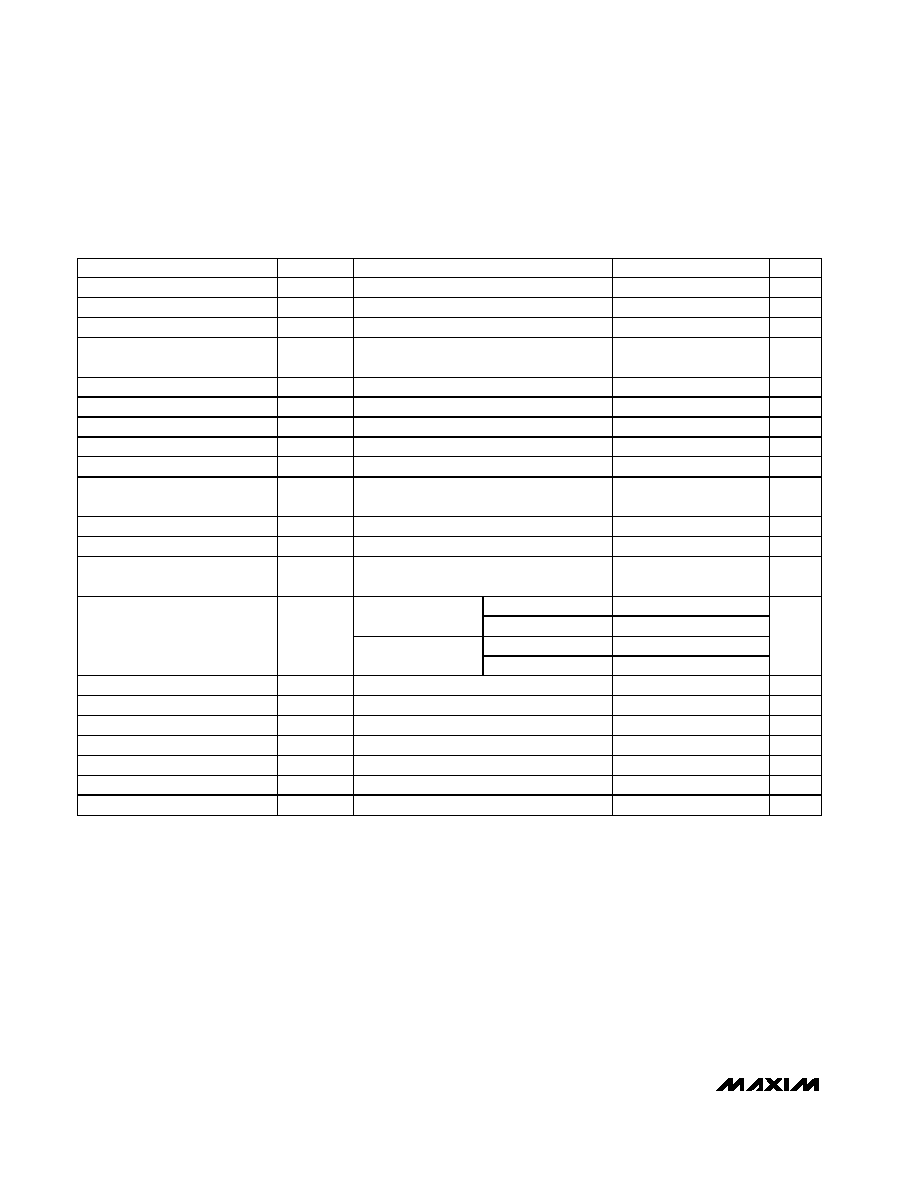
DRIVER DIFFERENTIAL DISTORTION
vs. FREQUENCY
MAX4361 toc01
FREQUENCY (Hz)
DIFFERENTIAL DISTORTION (dB)
100k
-90
-80
-70
-60
-50
-40
-100
10k
1M
V
OUT
= 7.2V
P-P
G = 3
R
L
= 12.5
3RD HARMONIC
2ND HARMONIC
MAX4361 toc02
PEAK-TO-PEAK OUTPUT VOLTAGE (V)
DIFFERENTIAL DISTORTION (dBc)
7
6
5
4
3
-90
-80
-70
-60
-50
-40
-100
2
8
DRIVER DIFFERENTIAL DISTORTION
vs. PEAK-TO-PEAK OUTPUT VOLTAGE
f = 100kHz
G = 3
R
L
= 12.5
9
3RD HARMONIC
2ND HARMONIC
MAX4361 toc03
R
LOAD
(
)
DIFFERENTIAL DISTORTION (dBc)
85
65
45
25
-90
-80
-70
-60
-100
5
DRIVER DIFFERENTIAL DISTORTION
vs. LOAD RESISTANCE
V
OUT
= 5V
P-P
f = 100kHz
G = 3
R
L
= 12.5
3RD HARMONIC
2ND HARMONIC
MAX4361 toc04
TRANSFORMER TURNS RATIO
P
LINE
(dBm)
4.8
4.6
4.2 4.4
3.4 3.6 3.8 4.0
3.2
10.5
11.0
11.5
12.0
12.5
13.0
13.5
14.0
14.5
15.0
15.5
16.0
10.0
3.0
5.0
DRIVER LINE POWER
vs. TURNS RATIO
V+ = 5.5V
V+ = 4.5V
V+ = 5V
FREQUENCY (Hz)
100k
10k
10
1M
1k
100
1
10
100
1
MAX4361 toc05
DRIVER CURRENT AND VOLTAGE NOISE
vs. FREQUENCY
INPUT CURRENT NOISE (pA/
Hz)
INPUT VOLTAGE NOISE (nV/
Hz)
V
NOISE
I
NOISE
MAX4361 toc06
FREQUENCY (Hz)
OUTPUT IMPEDANCE (
)
10M
1M
0.1
1
10
100
1k
10k
100k
0.01
100k
100M
DRIVER OUTPUT IMPEDANCE
vs. FREQUENCY
SHDN = V
CC
SHDN = GND
FREQUENCY (Hz)
GAIN (dB)
100M
10M
1M
100k
-25
-20
-15
-10
-5
0
5
10
15
20
-30
-150
-120
-90
-60
-30
0
30
60
90
120
-180
10k
1G
MAX4361 toc07
DRIVER GAIN AND PHASE
vs. FREQUENCY
PHASE (DEGREES)
GAIN
PHASE
G = 3
R
L
= 12.5
MAX4361 toc08
FREQUENCY (Hz)
PSRR (dB)
10M
1M
100k
10k
-70
-60
-50
-40
-30
-20
-10
0
10
-80
1k
1G
DRIVER POWER-SUPPLY REJECTION
RATIO vs. FREQUENCY
G = 1
DRIVER OUTPUT SWING
vs. LOAD RESISTANCE
MAX4361 toc09
LOAD RESISTANCE (
)
OUTPUT SWING (V)
1k
100
10
1.2
1.3
1.4
1.5
1.6
1.7
1.8
1.9
2.0
2.1
2.2
2.3
2.4
2.5
1.1
1
10k
1.0
-SWING
+SWING
Typical Operating Characteristics
(V+ = 5V, GND = 0, V
CM
= 2.5V, R
L
= 12.5
, SHDN = 0, T
A
= +25∞C.)