
General Description
The MAX4366 evaluation kit (EV kit) is a fully assembled
and tested circuit board that uses the MAX4366
bridged amplifier to drive speakers or headsets in
portable audio applications. The MAX4366 EV kit oper-
ates from a 2.3V to 5.5V DC power supply and is capa-
ble of delivering 330mW into a 32
load or 200mW into
a 16
load. The closed-loop gain of the MAX4366 is set
to 2V/V with external resistors. The MAX4367/MAX4368
bridged amplifiers with internal fixed gains can be eval-
uated on the MAX4366 EV kit. Contact Maxim to obtain
samples. The Selector Guide provides the complete
part numbers for the amplifiers that can be evaluated
on the MAX4366 EV kit.
Features
o Small 8-Pin SOT23 Package
o No DC-Blocking Capacitor On Output
o 2.3V to 5.5V Single-Supply Operation
o Drives 330mW into 32 Speakers or 200mW into
16
Speakers
o Externally Adjustable Gain
o Clickless/Popless Power-Up and Shutdown
o Fully Assembled and Tested
Evaluates: MAX4366/MAX4367/MAX4368
MAX4366 Evaluation Kit
________________________________________________________________ Maxim Integrated Products
1
19-2353; Rev 0; 2/02
Component List
For pricing, delivery, and ordering information, please contact Maxim/Dallas Direct! at
1-888-629-4642, or visit Maxim's website at www.maxim-ic.com.
Ordering Information
Selector Guide
DESIGNATION
QTY
DESCRIPTION
C1
1
10ĶF Ī10%, 6.3V X5R
ceramic capacitor (1206)
TDK C3216X5R0J106KT or
Taiyo Yuden
JMK316BJ106KL
C2
1
0.1ĶF Ī10%, 16V X7R
ceramic capacitor (0603)
TDK C1608X7R1C104KT or
Taiyo Yuden
EMK107BJ104KA
C3
1
1ĶF Ī10%, 6.3V X5R
ceramic capacitor (0603)
Taiyo Yuden
JMK107BJ105KA
C4
1
0.33ĶF Ī10%, 35V
tantalum capacitor (A)
Kemet T494A334K035AS
DESIGNATION
QTY
DESCRIPTION
C5
0
Not installed (0603)
R1, R2
2
20k
Ī1% resistors (0603)
R3
1
100k
Ī5% resistor (0603)
J1
1
Right-angle PC-mount phono
jack (white)
J2
1
2-position terminal block
JU1
1
3-pin header
U1
1
MAX4366, 8-pin SOT23
None
1
Shunt (JU1)
None
1
MAX4366 PC board
None
1
MAX4366 data sheet
None
1
MAX4366 EV kit data sheet
PART
TEMP RANGE
IC PACKAGE
MAX4366EVKIT
0įC to +70įC
8 SOT23
PART
GAIN
MAX4366
External
MAX4367
2V/V
MAX4368
3V/V
Evaluates: MAX4366/MAX4367/MAX4368
MAX4366 Evaluation Kit
2
_______________________________________________________________________________________
Quick Start
The MAX4366 EV kit is fully assembled and tested.
Follow the steps listed below to verify board operation.
Do not turn on the power supply until all connec-
tions are completed.
Recommended Equipment:
∑
5V, 1A power supply
∑
32
or 16 speaker
∑
Audio source (e.g., CD player, tape player)
1) Verify that a shunt is across pins 2 and 3 of jumper
JU1 (SHDN).
2) Connect an audio source to phono jack J1.
3) Connect the speaker across the + and ≠ outputs of
terminal block J2.
4) Connect the 5V terminal of the power supply to the
VCC pad and the ground terminal of the power sup-
ply to the GND pad.
5) Turn on the 5V power supply.
6) Turn on the audio source.
Detailed Description
The MAX4366 EV kit contains the MAX4366 bridged
amplifier designed to differentially drive speakers or
headsets in portable audio applications. The advantage
of driving speakers in a bridge-tied load (BTL) configu-
ration is that no large output capacitor is required and
the output voltage doubles compared to a single-ended
amplifier under similar conditions. Thus, the differential
gain of the device is twice the closed-loop gain of the
input amplifier. The MAX4366's input amplifier closed-
loop gain of 1V/V creates an effective gain of 2V/V
across the speaker.
The MAX4366 EV kit is capable of delivering the follow-
ing power when using the 5V power supply:
330mW to a 32
speaker and an input of 1.62V
RMS
200mW to a 16
speaker and an input of 0.894V
RMS
The MAX4366 EV kit operates from a 2.3V to 5.5V DC
power supply.
Output Signal
The MAX4366 EV kit produces a differential output sig-
nal that is used to drive 16
or 32 speakers. The pos-
itive and negative signals of the differential output are
180į out of phase and are both biased with a DC offset
of V
CC
/2. This bias voltage allows the voltage at the
load to swing between 0 and V
CC
. The MAX4366 EV kit
is configured for a gain of 2V/V. A feedback capacitor
(C5) may be added to limit the bandwidth or to com-
pensate for the parasitic capacitance at pin 4, especial-
ly at higher values of R2.
Shutdown
Jumper JU1 controls the shutdown pin (SHDN) on the
MAX4366. The shutdown function can also be con-
trolled by removing the shunt from JU1 and connecting
an external source to the SHDN pad. The SHDN pin is
an active-high pin that requires a low signal to enable
and a high signal to disable the MAX4366 EV kit (see
Table 1 for JU1 configuration).
Level Shifting
Jumper JU2 provides an option to use an external DC
source to level shift the output of the MAX4366 EV kit.
To use an external source for the DC component of the
output, connect the DC source to JU2.
Component Suppliers
SHUNT
POSITION
SHDN PIN
FUNCTION
1 and 2
Connected to VCC
Shutdown mode
2 and 3
Connected to GND
EV kit enabled
None*
Connect an external
source to SHDN pad
SHDN driven by
external source.
(SHDN pin is
active high)
Table 1. Jumper JU1 Configuration
SUPPLIER
PHONE
FAX
WEBSITE
Kemet
864-963-6300
864-963-6322
www.kemet.com
Taiyo Yuden
800-348-2496
847-925-0899
www.t-yuden.com
TDK
847-803-6100
847-390-4498
www.component.tdk.com
*Remove the shunt.
Note: Please indicate you are using the MAX4366 when contacting these component suppliers.
Setting the Gain
The signal gain of the MAX4366 input amplifier is set to
1V/V (BTL gain of 2V/V) with resistors R1 and R2. R1
and R2 set the gain of the amplifier as follows:
The gain of the device in a BTL configuration is twice
the gain of the single-ended case. Choose R1 and R2
between 10k
and 50k. The gains of the MAX4367/
MAX4368 are set internally.
Evaluating Other Amplifiers
The MAX4366 EV kit can be used to evaluate the
MAX4367/MAX4368 bridge amplifiers with fixed internal
gains. The MAX4367 has an internal gain of 2V/V and
the MAX4368 has an internal gain of 3V/V. Order sam-
ples of these amplifiers and replace the MAX4366 (U1)
on the board with the desired IC.
Note: Replace resistor R1 with a 0 resistor and remove
R2 to evaluate the amplifiers with internal gains.
A
2
R2
R1
VBTL
=
Evaluates: MAX4366/MAX4367/MAX4368
MAX4366 Evaluation Kit
_______________________________________________________________________________________
3
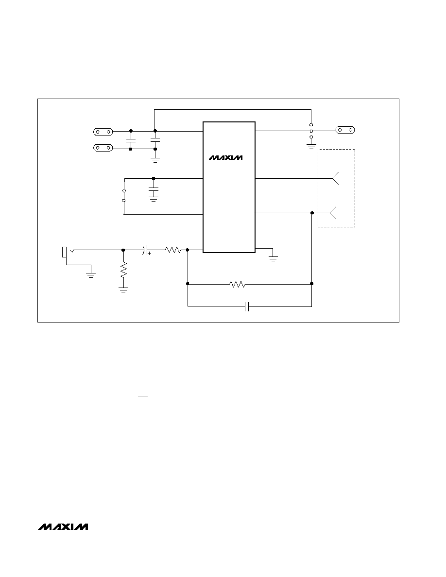
VCC
INPUT
R3
100k
R1
20k
1%
C3
1
ĶF
6
2
8
7
3
OUT-
BIAS
GND
MAX4366
U1
SHDN
OUT+
IN+
V
CC
IN-
4
1
5
SHDN
GND
R2
20k
1%
C4
0.33
ĶF
35V
C5
OPEN
C1
10
ĶF
C2
0.1
ĶF
JU2
J1
J2
OUTPUT
J2-1
J2-2
TERMINAL BLOCK
-
+
1
2
3
2
1
1
2
JU1
Figure 1. MAX4366 EV Kit Schematic
Maxim cannot assume responsibility for use of any circuitry other than circuitry entirely embodied in a Maxim product. No circuit patent licenses are
implied. Maxim reserves the right to change the circuitry and specifications without notice at any time.
4 _____________________Maxim Integrated Products, 120 San Gabriel Drive, Sunnyvale, CA 94086 408-737-7600
© 2002 Maxim Integrated Products
Printed USA
is a registered trademark of Maxim Integrated Products.
Evaluates: MAX4366/MAX4367/MAX4368
MAX4366 Evaluation Kit
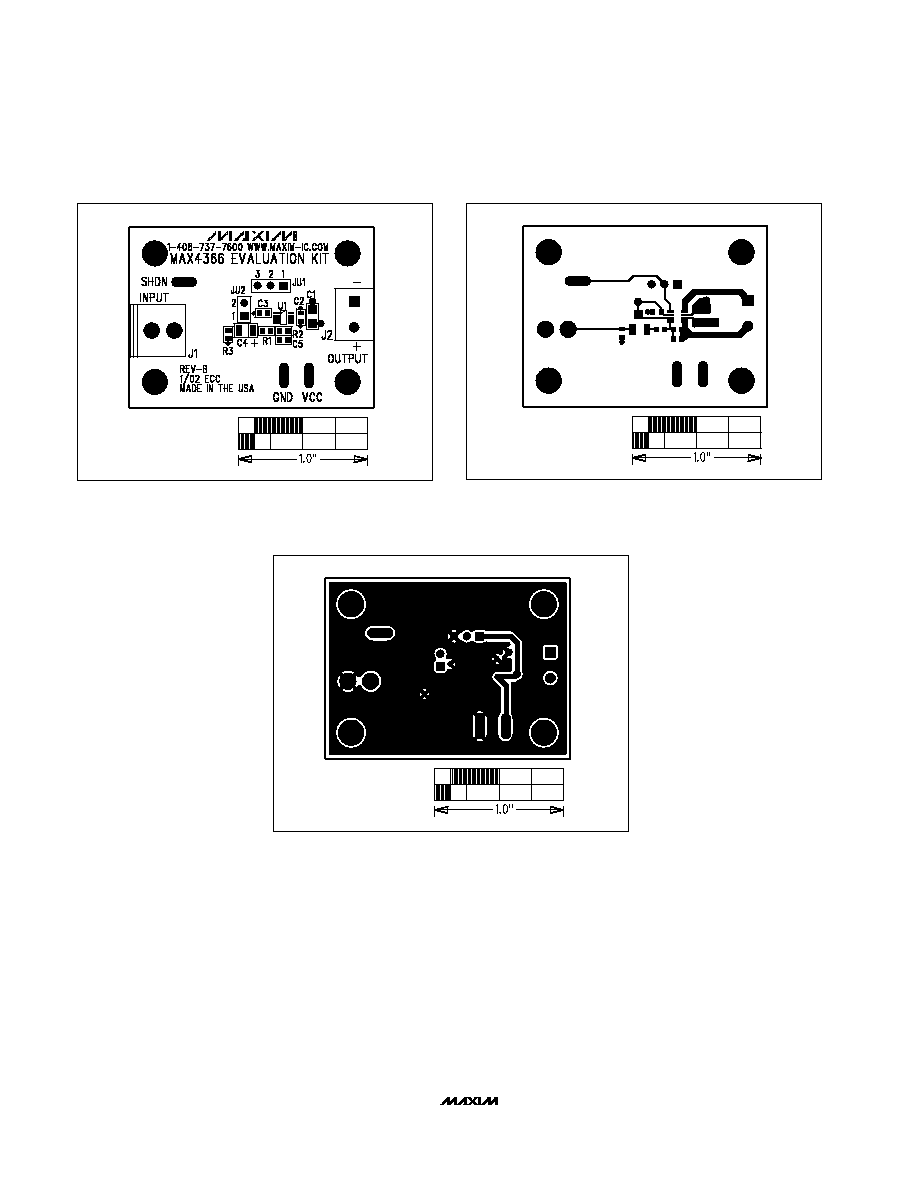
Figure 2. MAX4366 EV Kit Component Placement Guide--
Component Side
Figure 3. MAX4366 EV Kit PC Board Layout--Component Side
Figure 4. MAX4366 EV Kit PC Board Layout--Solder Side