 | –≠–ª–µ–∫—Ç—Ä–æ–Ω–Ω—ã–π –∫–æ–º–ø–æ–Ω–µ–Ω—Ç: MAX4436 | –°–∫–∞—á–∞—Ç—å:  PDF PDF  ZIP ZIP |
General Description
The MAX4434/MAX4435 single and MAX4436/MAX4437
dual operational amplifiers feature wide bandwidth, 16-
bit settling time in 23ns, and low-noise/low-distortion
operation. The MAX4434/MAX4436 are compensated for
unity-gain stability and have a small-signal -3dB band-
width of 150MHz. The MAX4435/MAX4437 are compen-
sated for closed-loop gains of +5 or greater and have a
small-signal, -3dB bandwidth of 150MHz.
The MAX4434≠MAX4437 op amps require only 15mA of
supply current per amplifier while achieving 115dB
open-loop gain. Voltage noise density is a low 2.2nV/
Hz
and provides 97dB spurious-free dynamic range (SFDR)
at 1MHz. These characteristics make these op amps
ideal for driving modern, high-speed 14- and 16-bit ana-
log-to-digital converters (ADCs).
These high-speed op amps feature wide-output voltage
swings and a high-current output drive up to 65mA. Using
a voltage feedback architecture, the MAX4434≠
MAX4437 meet the requirements of many applications
that previously depended on current feedback amplifiers.
The MAX4434/MAX4435 are available in space-saving
5-pin SOT23 packages and the MAX4436/MAX4437 are
available in 8-pin µMAX packages.
________________________Applications
High-Speed 14- and 16-Bit ADC Preamplifiers
Low-Noise Preamplifiers
IF/RF Amplifiers
Low-Distortion Active Filters
High-Performance Receivers
Precision Instrumentation
____________________________Features
o 16-Bit Accurate Settling in 23ns
(MAX4435/MAX4437)
o 97dB SFDR at 1MHz, 4Vp-p Output
o 2.2nV/Hz Input Voltage Noise Density
o 100dB (min) Open-Loop Gain
o 388V/µs Slew Rate (MAX4435/MAX4437)
o 65mA High Output Drive
o Available in Space-Saving Packages
5-Pin SOT23 (MAX4434/MAX4435)
8-Pin µMAX (MAX4436/MAX4437)
MAX4434≠MAX4437
Single-Supply, 150MHz, 16-Bit Accurate,
Ultra-Low Distortion Op Amps
________________________________________________________________ Maxim Integrated Products
1
19-2200; Rev 0; 10/01
For pricing, delivery, and ordering information, please contact Maxim/Dallas Direct! at
1-888-629-4642, or visit Maxim's website at www.maxim-ic.com.
Ordering Information
Selector Guide appears at end of data sheet.
IN-
IN+
1
5
V
CC
OUT
MAX4434
MAX4435
SOT23-5
TOP VIEW
2
3
4
V
EE
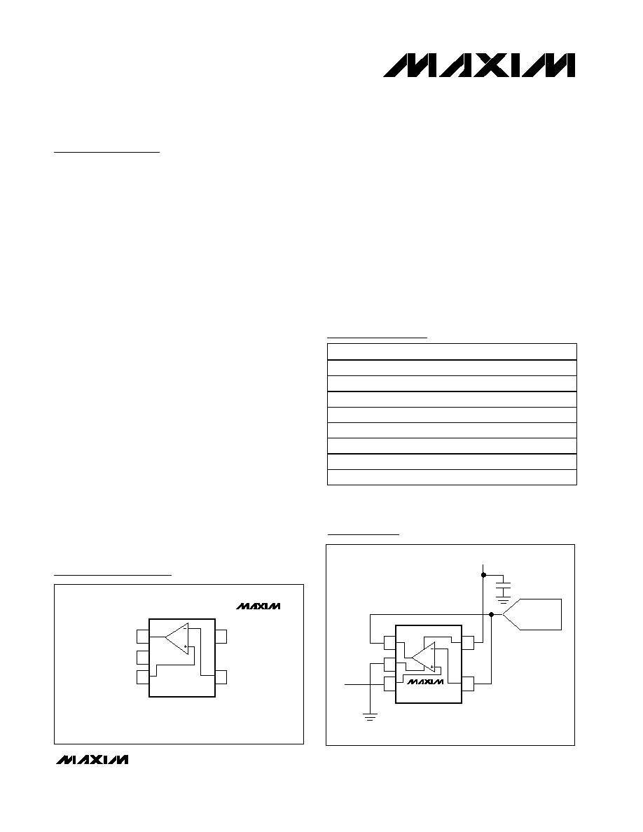
Pin Configurations
Typical Operating Circuit
IN
1
5
V
CC
2
3
4
C
1
HIGH-SPEED
14-/16-BIT ADC
MAX4434
MAX4435
Pin Configurations continued at end of data sheet.
PART
TEMP. RANGE
PIN-PACKAGE
MAX4434EUK-T
-40∞C to +85∞C
5 SOT23-5
MAX4434ESA
-40∞C to +85∞C
8 SO
MAX4435EUK-T
-40∞C to +85∞C
5 SOT23-5
MAX4435ESA
-40∞C to +85∞C
8 SO
MAX4436EUA
-40∞C to +85∞C
8 µMAX
MAX4436ESA
-40∞C to +85∞C
8 SO
MAX4437EUA
-40∞C to +85∞C
8 µMAX
MAX4437ESA
-40∞C to +85∞C
8 SO
MAX4434≠MAX4437
Single-Supply, 150MHz, 16-Bit Accurate,
Ultra-Low Distortion Op Amps
2
_______________________________________________________________________________________
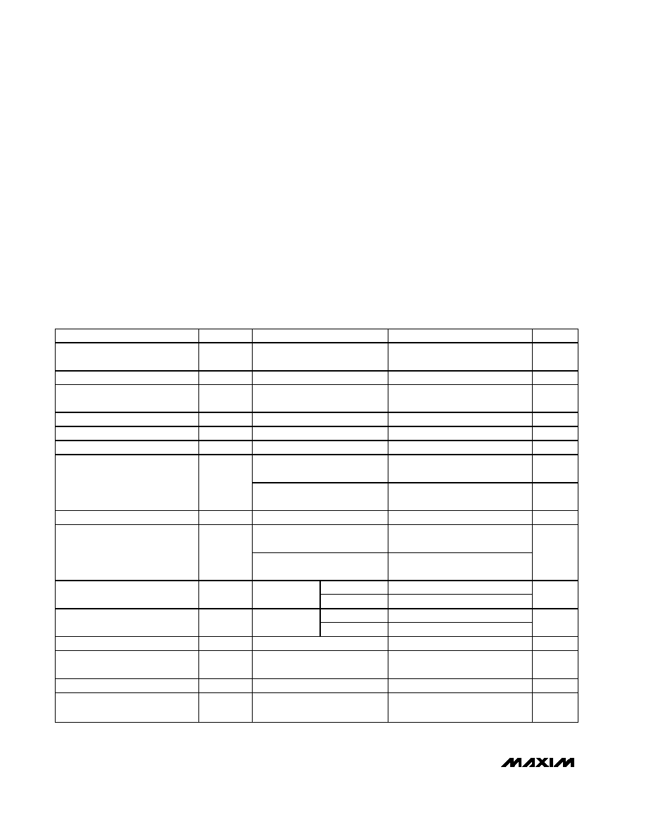
ABSOLUTE MAXIMUM RATINGS
DC ELECTRICAL CHARACTERISTICS
(V
CC
= +5V, V
EE
= 0, R
L
=
to V
CC
/2, T
A
= T
MIN
to T
MAX
, unless otherwise noted. Typical values are at T
A
= +25∞C.) (Note 2)
Stresses beyond those listed under "Absolute Maximum Ratings" may cause permanent damage to the device. These are stress ratings only, and functional
operation of the device at these or any other conditions beyond those indicated in the operational sections of the specifications is not implied. Exposure to
absolute maximum rating conditions for extended periods may affect device reliability.
Supply Voltage (V
CC
- V
EE
) ...................................................+6V
Differential Input Voltage .......................................................+2V
Input Voltage Range ........................(V
CC
+ 0.3V) to (V
EE
- 0.3V)
Current into Any Input Pin.................................................±25mA
Output Short-Circuit Duration to V
CC
or V
EE
...................(Note 1)
Continuous Power Dissipation (T
A
= +70∞C)
5-Pin SOT23 (derate 7.1mW/∞C above +70∞C) ..........571mW
8-Pin SO (derate 5.88mW/∞C above +70∞C)...............471mW
8-Pin µMAX (derate 4.5mW/∞C above +70∞C) ........... 330mW
Operating Temperature Range ...........................-40∞C to +85∞C
Junction Temperature ......................................................+150∞C
Storage Temperature Range .............................-65∞C to +150∞C
Lead Temperature (soldering, 10s) .................................+300∞C
Note 1: The MAX4434≠MAX4437 are not protected for output short-circuit conditions.
PARAMETER
SYMBOL
CONDITIONS
MIN
TYP
MAX
UNITS
Input Common-Mode Voltage
Range
V
CM
Guaranteed by CMRR test
V
EE
V
CC
- 1
V
Input Offset Voltage
V
OS
1
3.5
mV
Input Offset Voltage
Temperature Coefficient
TCV
OS
4
µV/∞C
Input Offset Voltage Matching
MAX4436/MAX4437
0.25
mV
Input Bias Current
I
B
14
22
µA
Input Offset Current
I
OS
1
5
µA
Differential Mode
-10mV
V
IN
+10mV
1
k
Input Resistance
R
IN
Common Mode
0
V
CM
(V
CC
- 1V)
1.7
M
Common-Mode Rejection Ratio
CMRR
V
EE
V
CM
(V
CC
- 1V)
75
100
dB
(V
EE
+ 0.25)
V
OUT
(V
CC
-
0.25), R
L
= 10k
100
115
Open-Loop Gain
A
VOL
(V
EE
+ 0.5)
V
OUT
(V
CC
-
0.5), R
L
= 500
96
110
dB
V
CC
- V
OH
65
200
Output Voltage Swing
V
OUT
R
L
= 10k
V
OL
- V
EE
15
70
mV
Sinking
40
65
Output Current
I
OUT
R
L
= 20
to
Ground
Sourcing
35
60
mA
Output Short-Circuit Current
I
SC
Sinking or sourcing
±70
mA
DC Power-Supply Rejection
Ratio
PSRR
V
CC
= +4.5V to +5.5V
85
110
dB
Operating Supply Voltage
V
S
Guaranteed by PSRR test
+4.5
+5.5
V
Quiescent Supply Current
(Per Amplifier)
I
S
15
18
mA
Note 2: All devices are 100% production tested at +25∞C. Specifications over temperature limits are guaranteed by design.

MAX4434≠MAX4437
Single-Supply, 150MHz, 16-Bit Accurate,
Ultra-Low Distortion Op Amps
_______________________________________________________________________________________
3
AC ELECTRICAL CHARACTERISTICS
(V
CC
= +5V, V
EE
= 0, V
CM
= V
CC
/2, R
L
= 500
, A
VCL
= +1, and T
A
= +25∞C, unless otherwise noted.)
PARAMETER
SYMBOL
CONDITIONS
MIN
TYP
MAX
UNITS
V
OUT
= 20mVp-p
MAX4434/MAX4436
150
Small-Signal -3dB
Bandwidth
BW
SS
V
OUT
= 20mVp-p
MAX4435/MAX4437 (A
VCL
= +5)
150
MHz
V
OUT
= 2Vp-p
MAX4434/MAX4436
28
Large-Signal -3dB
Bandwidth
BW
LS
V
OUT
= 4Vp-p
MAX4435/MAX4437 (A
VCL
= +5)
25
MHz
V
OUT
= 20mVp-p
MAX4434/MAX4436
80
Small-Signal 0.1dB
Gain Flatness
BW
0.1dBSS
V
OUT
= 20mVp-p
MAX4435/MAX4437 (A
VCL
= +5)
80
MHz
V
OUT
= 2Vp-p
MAX4434/MAX4436
15
Large-Signal 0.1dB
Gain Flatness
BW
0.1dBLS
V
OUT
= 4Vp-p
MAX4435/MAX4437 (A
VCL
= +5)
20
MHz
V
OUT
= 2V step
MAX4434/MAX4436
133
Slew Rate
SR
V
OUT
= 4V step
MAX4435/MAX4437 (A
VCL
= +5)
388
V/µs
V
OUT
= 2V step
MAX4434/MAX4436
17
Rise/Fall Time
t
R
, t
F
V
OUT
= 4V step
MAX4435/MAX4437 (A
VCL
= +5)
10
ns
V
OUT
= 1.5V to 3.5V step
MAX4434/MAX4436
35
V
OUT
= 1.5V to 3.5V step
MAX4435/MAX4437 (A
VCL
= +5)
23
Settling Time to 16-Bit
(0.0015%)
t
S 0.0015%
V
OUT
= 1V to 4V step
MAX4434/MAX4436
42
ns
Output "Glitch" Settling
to 16-Bit (0.0015%)
5pF load, C
L
charged from 1V to 4V
41
ns
Output Overload
Recovery Time
50% overdrive, settling to 10% accuracy
100
ns
AC Common-Mode
Rejection Ratio
CMRR
f
C
= 100kHz
-92
dB
Typical Operating Characteristics
(V
CC
= +5V, V
EE
= 0, R
L
= 500
, C
L
= 0, T
A
= +25∞C, unless otherwise noted.)
MAX4434≠MAX4437
Single-Supply, 150MHz, 16-Bit Accurate,
Ultra-Low Distortion Op Amps
4
_______________________________________________________________________________________
-7
-4
-5
-6
-3
-2
-1
0
1
2
3
100k
1M
10M
100M
1G
MAX4434/MAX4436
SMALL-SIGNAL GAIN vs. FREQUENCY
(A
VCL
= +1V/V)
MAX4434-37 toc01
FREQUENCY (Hz)
GAIN (dB)
20mVp-p
-7
-4
-5
-6
-3
-2
-1
0
1
2
3
100k
1M
10M
100M
1G
MAX4435/MAX4437
SMALL-SIGNAL GAIN vs. FREQUENCY
(A
VCL
= +5V/V)
MAX4434-37 toc02
FREQUENCY (Hz)
GAIN (dB)
20mVp-p
-0.7
-0.4
-0.5
-0.6
-0.3
-0.2
-0.1
0
0.1
0.2
0.3
100k
1M
10M
100M
1G
MAX4434/MAX4436
GAIN FLATNESS vs. FREQUENCY
(A
VCL
= +1V/V)
MAX4434-37 toc03
FREQUENCY (Hz)
GAIN (dB)
20mVp-p
PARAMETER
SYMBOL
CONDITIONS
MIN
TYP
MAX
UNITS
AC Power-Supply
Rejection Ratio
PSRR
f
C
= 100kHz
-101
dB
f
C
= 100kHz
-97
V
OUT
= 2Vp-p
centered at V
CC
/2
f
C
= 1MHz
-98
f
C
= 100kHz
-130
V
OUT
= 3Vp-p
centered at V
CC
/2
f
C
= 1MHz
-99
f
C
= 100kHz
-112
Spurious-Free Dynamic
Range
SFDR
V
OUT
= 4Vp-p
centered at V
CC
/2
f
C
= 1MHz
-97
dBc
Input Noise Voltage
Density
en
f
C
= 100kHz
2.2
nV/
Hz
Input Noise Current
Density
in
f
C
= 100kHz
2.0
pA/
Hz
Input Capacitance
C
IN
2.3
pF
Maximum Capacitive
Load Without Sustained
Oscillations
30
pF
Output Impedance
Z
OUT
f
C
= 1MHz
0.05
Crosstalk
f
C
= 1MHz, MAX4436/MAX4437
-80
dB
AC ELECTRICAL CHARACTERISTICS (continued)
(V
CC
= +5V, V
EE
= 0, V
CM
= V
CC
/2, R
L
= 500
, A
VCL
= +1, and T
A
= +25∞C, unless otherwise noted.)

MAX4434≠MAX4437
Single-Supply, 150MHz, 16-Bit Accurate,
Ultra-Low Distortion Op Amps
_______________________________________________________________________________________
5
-0.7
-0.4
-0.5
-0.6
-0.3
-0.2
-0.1
0
0.1
0.2
0.3
100k
1M
10M
100M
MAX4434/MAX4436
GAIN FLATNESS vs. FREQUENCY
(A
VCL
= +1V/V)
MAX4434-37 toc04
FREQUENCY (Hz)
GAIN (dB)
2Vp-p
10M
MAX4435/MAX4437
GAIN FLATNESS vs. FREQUENCY
(A
VCL
= +5V/V)
0.3
-0.1
MAX4434-37 toc05
-0.3
-0.4
-0.5
-0.6
-0.7
-0.2
0.2
0.1
0
100k
1M
100M
1G
FREQUENCY (Hz)
GAIN (dB)
-0.7
-0.4
-0.5
-0.6
-0.3
-0.2
-0.1
0
0.1
0.2
0.3
100k
1M
10M
100M
MAX4435/MAX4437
GAIN FLATNESS vs. FREQUENCY
(A
VCL
= +5V/V)
MAX4434-37 toc06
FREQUENCY (Hz)
GAIN (dB)
4Vp-p
MAX4434/MAX4436
LARGE-SIGNAL GAIN vs. FREQUENCY
(A
VCL
= +1V/V)
3
-1
MAX4434-37 toc07
-3
-4
-5
-6
-7
-2
2
1
0
100k
1M
10M
100M
FREQUENCY (Hz)
GAIN (dB)
2Vp-p
-7
-4
-5
-6
-3
-2
-1
0
1
2
3
100k
1M
10M
100M
MAX4435/MAX4437
LARGE-SIGNAL GAIN vs. FREQUENCY
(A
VCL
= +5V/V)
MAX4434-37 toc08
FREQUENCY (Hz)
GAIN (dB)
MAX4434/MAX4436
SMALL-SIGNAL PULSE RESPONSE
MAX4434-47 toc09
INPUT
50mV/div
OUTPUT
50mV/div
20ns/div
A
VCL
= +1V/V
MAX4435/MAX4437
SMALL-SIGNAL PULSE RESPONSE
MAX4434-47 toc10
INPUT
10mV/div
OUTPUT
50mV/div
20ns/div
A
VCL
= +5V/V
MAX4434/MAX4436
LARGE-SIGNAL PULSE RESPONSE
MAX4434-47 toc11
INPUT
1V/div
OUTPUT
1V/div
20ns/div
A
VCL
= +1V/V
MAX4435/MAX4437
LARGE-SIGNAL PULSE RESPONSE
MAX4434-47 toc12
INPUT
200mV/div
OUTPUT
1V/div
20ns/div
A
VCL
= +5V/V
Typical Operating Characteristics (continued)
(V
CC
= +5V, V
EE
= 0, R
L
= 500
, C
L
= 0, T
A
= +25∞C, unless otherwise noted.)