 | –≠–ª–µ–∫—Ç—Ä–æ–Ω–Ω—ã–π –∫–æ–º–ø–æ–Ω–µ–Ω—Ç: MAX4456 | –°–∫–∞—á–∞—Ç—å:  PDF PDF  ZIP ZIP |

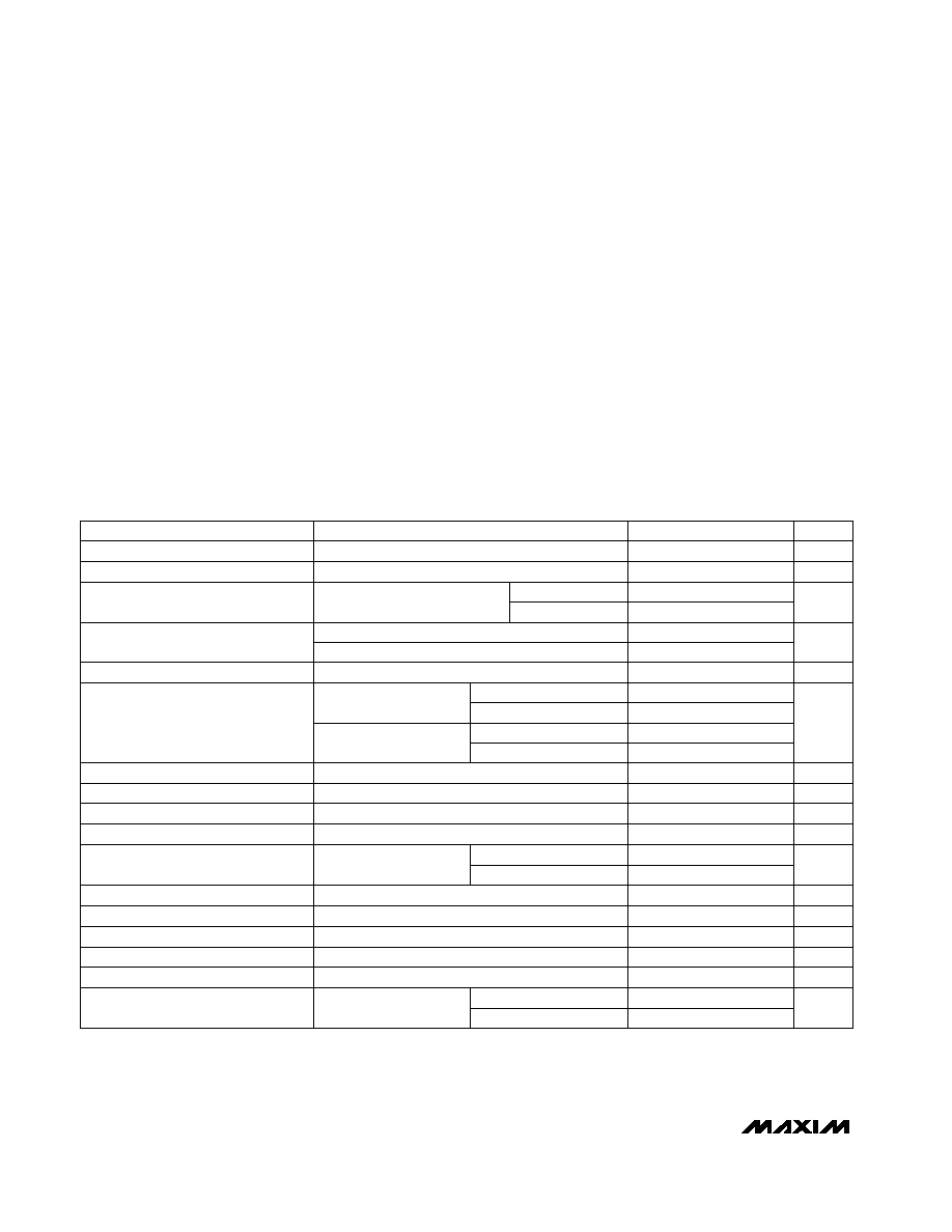
General Description
The MAX4359/MAX4360/MAX4456 low-cost video cross-
point switches are designed to reduce component count,
board space, design time, and system cost. Each con-
tains a matrix of T-switches that connect any of their four
(MAX4359) or eight (MAX4360/MAX4456) video inputs to
any of their buffered outputs, in any combination. Each
matrix output is buffered by an internal, high-speed
(250V/µs), unity-gain amplifier that is capable of driving
400
and 20pF at 2.6Vp-p. For applications requiring
increased drive capability, buffer the MAX4359/
MAX4360/MAX4456 outputs with the MAX497 quad,
gain-of-two video line driver.
The MAX4456 has a digitally controlled 8x8 switch matrix
and is a low-cost pin-for-pin compatible alternative to the
popular MAX456. The MAX4359/MAX4360 are similar to
the MAX4456, with the 8x8 switch matrix replaced by a
4x4 (MAX4359) or an 8x4 (MAX4360) switch matrix.
Three-state output capability and internal, programmable
active loads make it feasible to parallel multiple devices
to form larger switch arrays. The inputs and outputs are
on opposite sides, and a quiet power supply or digital
input line separates each channel, which reduces
crosstalk to -70dB at 5MHz. For applications demanding
better DC specifications, see the MAX456 8x8 video
crosspoint switch.
________________________ Applications
Features
o Eight (MAX4456) or Four (MAX4359/MAX4360)
Internal Buffers
250V/µs Slew Rate
Three-State Output Capability
Power-Saving Disable Feature
65MHz -3dB Bandwidth
o Routes Any Input Channel to Any Output Channel
o Serial or Parallel Digital Interface
o Expandable for Larger Switch Matrices
o 80dB All-Channel Off-Isolation at 5MHz
o 70dB Single-Channel Crosstalk
o Straight-Through Pinouts Simplify Layout
o Low-Cost Pin-Compatible Alternative to
MAX456 (MAX4456)
MAX4359/MAX4360/MAX4456
Low-Cost 4x4, 8x4, 8x8
Video Crosspoint Switches
________________________________________________________________ Maxim Integrated Products
1
OUTPUT
SELECT
4x4
(8x4)
T-SWITCH
MATRIX
MAX497
4 INPUT CHANNELS
(8 INPUT CHANNELS)
A1
A0
D3
D2
D1/SER OUT
D0/SER IN
INPUT
SELECT
OR
SERIAL
I/O
MAX4359
(MAX4360)
LATCH
WR
75
75
A
V
= +2
Z
0
= 75
Z
0
= 75
(MAX4360)
OUTPUT
SELECT
8x8
T-SWITCH
MATRIX
MAX497
A2
8 INPUT CHANNELS
A1
A0
D3
D2
D1/SER OUT
D0/SER IN
INPUT
SELECT
OR
SERIAL
I/O
MAX4456
LATCH
WR
75
75
A
V
= +2
MAX497
A
V
= +2
_________________________________________________ Typical Application Circuits
19-1389; Rev 1; 12/99
High-Speed Signal
Routing
Video-On-Demand
Systems
Video Test Equipment
Video Conferencing
Security Systems
Ordering Information
For free samples & the latest literature: http://www.maxim-ic.com, or phone 1-800-998-8800.
For small orders, phone 1-800-835-8769.
Pin Configurations appear at end of data sheet.
MAX4456EQH
-40∞C to +85∞C
44 PLCC
MAX4456EPL
-40∞C to +85∞C
40 Plastic DIP
MAX4456CPL
0∞C to +70∞C
40 Plastic DIP
MAX4456CQH
0∞C to +70∞C
44 PLCC
MAX4360EAX
-40∞C to +85∞C
36 SSOP
MAX4359EAX
-40∞C to +85∞C
36 SSOP
MAX4359EWG
-40∞C to +85∞C
24 SO
PART
TEMP. RANGE
PIN-PACKAGE
MAX4359/MAX4360/MAX4456
Low-Cost 4x4, 8x4, 8x8
Video Crosspoint Switches
2
_______________________________________________________________________________________
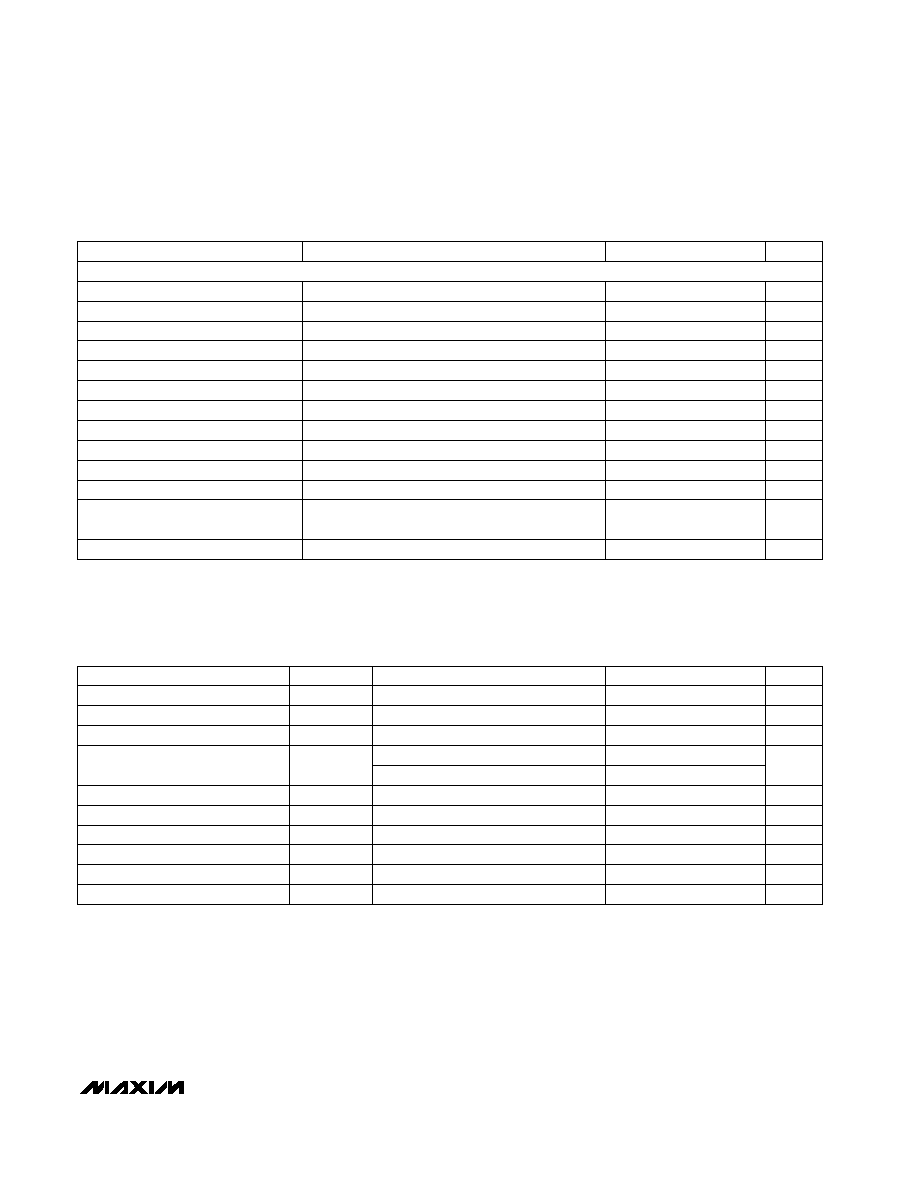
DC ELECTRICAL CHARACTERISTICS
(V+ = +5V, V- = -5V, V
LOAD
= +5V (internal load resistors on), V
IN_
= V
AGND
= V
DGND
= 0, T
A
= T
MIN
to T
MAX
, unless otherwise noted.
Typical values are at T
A
= +25∞C.)
Stresses beyond those listed under "Absolute Maximum Ratings" may cause permanent damage to the device. These are stress ratings only, and functional
operation of the device at these or any other conditions beyond those indicated in the operational sections of the specifications is not implied. Exposure to
absolute maximum rating conditions for extended periods may affect device reliability.
PARAMETER
CONDITIONS
MIN
TYP
MAX
UNITS
MAX4359/MAX4360
20
32
Offset Voltage Drift
20
µV/∞C
Buffer Offset Voltage
T
A
= +25∞C
±1
±15
Supply Current, All Buffers On
(no external load)
37
mA
Supply Current, All Buffers Off
1.6
5
mA
Power-Supply Rejection Ratio
±4.5V to ±5.5V
50
64
dB
Operating Supply Voltage
Inferred from PSRR test
±4.5
±5.5
V
0.99
1.0
1.01
Voltage Gain
V/V
Analog Input Current
±0.1
±100
nA
Output Leakage Current
Internal load resistors off, all buffers off
±100
nA
T
A
= T
MIN
to T
MAX
±20
mV
V
LOAD
= 5V
250
400
600
Internal Amplifier Load Resistor
200
765
Digital Input Current
±1
Output Impedance at DC
10
Input Logic Low Threshold
0.8
V
Input Logic High Threshold
2.4
V
0.4
4
V
Serial mode,
V
SER/PAR
= 5V
µA
Buffer Output Voltage Swing
Internal load resistors on, no external load
±1.3
V
Total Supply Voltage (V+ to V-) ...........................................+12V
Positive Supply Voltage (V+) Referred to AGND .......-0.3V to +12V
Negative Supply Voltage (V-) Referred to AGND ......-12V to +0.3V
DGND to AGND ..................................................................±0.3V
Buffer Short Circuit to Ground when
Not Exceeding Package Power Dissipation .............Indefinite
Analog Input Voltage ............................(V+ + 0.3V) to (V- - 0.3V)
Digital Input Voltage .............................(V+ + 0.3V) to (V- - 0.3V)
Input Current, Power On or Off
Digital Inputs.................................................................±20mA
Analog Inputs ...............................................................±50mA
Continuous Power Dissipation (T
A
= +70∞C)
36-Pin SSOP (derate 11.8mW/∞C above +70∞C) ...........941mW
24-Pin SO (derate 11.8mW/∞C above +70∞C)................941mW
40-Pin Plastic DIP (derate 11.3mW/∞C above +70∞C)....889mW
44-Pin PLCC (derate 13.3mW/∞C above +70∞C) .......1066mW
Operating Temperature Ranges
MAX4456C _ _ ....................................................0∞C to +70∞C
MAX4_ _ _E_ _ .................................................-40∞C to +85∞C
Junction Temperature ......................................................+150∞C
Storage Temperature Range .............................-65∞C to +150∞C
Lead Temperature (soldering, 10sec) .............................+300∞C
ABSOLUTE MAXIMUM RATINGS
Internal load resistors on,
no external load, V
IN
= 0 to 1V
I
OL
= 0.4mA
I
OH
= -0.4mA
T
A
= +25∞C
T
A
= T
MIN
to T
MAX
0.98
1.0
1.02
Input Voltage Range
Inferred from swing test
-1.3
1.3
V
SER OUT Output Logic Low/High
MAX4456
39
50
65
T
A
= T
MIN
to T
MAX
T
A
= +25∞C
T
A
= T
MIN
to T
MAX
T
A
= +25∞C
T
A
= T
MIN
to T
MAX
T
A
= +25∞C
MAX4359/MAX4360/MAX4456
Low-Cost 4x4, 8x4, 8x8
Video Crosspoint Switches
_______________________________________________________________________________________
3
Note 1: See Dynamic Test Circuits section.
Note 2: 3dB typical crosstalk improvement when R
S
= 0.
Note 3: Input test signal: 3.58MHz sine wave of amplitude 40IRE superimposed on a linear ramp (0 to 100IRE). IRE is a unit of
video-signal amplitude developed by the International Radio Engineers. 140IRE = 1.0V.
Note 4: Guaranteed by design.
PARAMETER
CONDITIONS
MIN
TYP
MAX
UNITS
All-Hostile Crosstalk
5MHz, V
IN
= 2Vp-p (Notes 1, 2)
57
dB
Output-Buffer Slew Rate
X
Internal load resistors on, 10pF load
250
V/µs
Single-Channel Crosstalk
5MHz, V
IN
= 2Vp-p (Note 1)
70
dB
All-Channel Off-Isolation
5MHz, V
IN
= 2Vp-p (Note 1)
80
dB
-3dB Bandwidth
10pF load, V
IN
= 2Vp-p (Note 1)
35
MHz
Differential Phase Error
(Note 3)
1.0
degrees
Differential Gain Error
(Note 3)
0.5
%
Input Noise
DC to 40MHz
0.3
mV
RMS
Input Capacitance
All buffer inputs grounded
6
pF
Buffer Input Capacitance
Additional capacitance for each output buffer
connected to channel input
2
pF
Output Capacitance
Output buffer off
7
pF
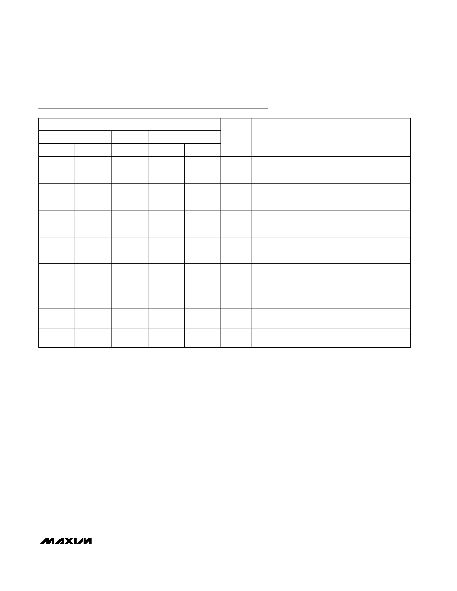
PARAMETER
Latch Delay
SYMBOL
MIN
TYP MAX
t
D
80
UNITS
ns
Switch Break-Before-Make Delay
t
ON -
t
OFF
15
ns
LATCH Edge to Switch Off
t
OFF
35
ns
LATCH Edge to Switch On
t
ON
50
ns
Write Pulse Width Low
t
WL
80
ns
Chip-Enable to Write Setup
t
CE
0
ns
Write Pulse Width High
t
WH
80
ns
240
Data Hold
t
DH
0
ns
Latch Pulse Width
t
L
80
ns
CONDITIONS
LATCH on
Parallel mode
Serial mode
Data Setup
t
DS
160
ns
SWITCHING CHARACTERISTICS
(Figure 4, V+ = +5V, V- = -5V, V
LOAD
= +5V (internal load resistors on), V
IN_
= V
AGND
= V
DGND
= 0, T
A
= T
MIN
to T
MAX
, unless other-
wise noted. Typical values are at T
A
= +25∞C.) (Note 4)
AC ELECTRICAL CHARACTERISTICS
(V+ = +5V, V- = -5V, V
LOAD
= +5V (internal load resistors on), V
AGND
= V
DGND
= 0, T
A
= +25∞C, unless otherwise noted.)
Small-Signal -3dB Bandwidth
10pF load, V
IN
= 100mVp-p (Note 1)
65
MHz
0.1dB Bandwidth
10pF load, V
IN
= 100mVp-p (Note 1)
4
MHz
DYNAMIC SPECIFICATIONS

MAX4359/MAX4360/MAX4456
Low-Cost 4x4, 8x4, 8x8
Video Crosspoint Switches
4
_______________________________________________________________________________________
Pin Description
2
2
2
Parallel Data Bit D0 when SER/PAR = GND. Serial
input when SER/PAR = V
CC
.
3, 5
3, 5
3, 5
Output Buffer Address Lines
4, 6, 8, 10
4, 6, 8, 10
4, 6, 8, 10,
12, 14, 16,
18
Video Input Lines
7
7
7
Asynchronous Control Line. When LOAD = V
CC
, all the
400
internal active loads are on. When LOAD = GND,
external 400
loads must be used. The buffers must
have a resistive load to maintain stability.
9
9
9
Digital Ground. DGND pins must have the same
potential and be bypassed to AGND. DGND should
be within ±0.3V of AGND.
11
11
11
When this control line is high, the 2nd-rank registers
are loaded with the rising edge of LATCH. If this con-
trol line is low, the 2nd-rank registers are transparent
when LATCH is low, passing data directly from the
1st-rank registers to the decoders.
--
12≠16, 18,
22≠26
22≠26
No connection. Not internally connected.
12
17
17
Connect to V
CC
for serial mode; connect to GND for
parallel mode.
13
19, 30
19, 30
Negative Supply. All V- pins must be connected to each
other and bypassed to GND separately (Figure 2).
14
20
20
In serial mode, WR (write) shifts data into the input regis-
ter. In parallel mode, WR loads data into the 1st-rank
registers. Data is latched on the rising edge.
1
2
1
1
1
Parallel Data Bit D1 when SER/PAR = GND. Serial out-
put for cascading multiple parts when SER/PAR = V
CC
.
D1/
SER OUT
2
3
3, 4, 6
4, 5, 7
5, 7, 9, 11,
13, 15, 17,
19
6, 8, 10, 13,
15, 17, 19,
21
8
9
10, 12
11, 14
14
16
--
1, 12, 23,
34
18
20
20, 34
22, 38
21
24
D0/SER IN
A_
IN_
LOAD
DGND
EDGE/
LEVEL
N.C.
SER/PAR
V-
WR
MAX4360
MAX4456
MAX4359
DIP
PLCC
SO
SSOP
SSOP
FUNCTION
NAME
PIN
15
21
21
If EDGE/LEVEL = V
CC
, data is loaded from the 1st-
rank registers to the 2nd-rank registers on the rising
edge of LATCH. If EDGE/LEVEL = GND, data is
loaded while LATCH = GND. In addition, data is
loaded during the execution of parallel-mode func-
tions 1011 through 1110, or if LATCH = V
CC
during
the execution of the parallel-mode "software-latch"
command (1111).
22
25
LATCH
MAX4359/MAX4360/MAX4456
Low-Cost 4x4, 8x4, 8x8
Video Crosspoint Switches
_______________________________________________________________________________________
5
Pin Description (continued)
V+
D2
D3
AGND
OUT_
CE
CE
18, 29, 44
16, 26, 40
42
38
40
36
31, 33, 36
28, 30, 32
28, 30, 32,
35, 37, 39,
41, 43
25, 27, 29,
31, 33, 35,
37, 39
27
24
26
23
Positive Supply. All V+ pins must be connected to each
other and bypassed to AGND separately (Figure 2).
13, 36
36
24
Parallel Data Bit D2 when SER/PAR = GND. Not used
when SER/PAR = V
CC
.
34
34
22
Parallel Data Bit when SER/PAR = GND. When
D3 = GND, D0≠D2 specify the input channel to be con-
nected to specified buffer. When D3 = V
CC
, D0≠D2
specify control codes. D3 is not used in serial mode
(SER/PAR = V
CC
).
32
32
20
Analog Ground. AGND must be at 0.0V, since the gain-
setting resistors of the buffers are connected to these
pins.
15, 29
29
18
Buffer Outputs. Buffer inputs are internally grounded with
a 1000 or 1001 command from the D3≠D0 lines.
28, 31, 33,
35
28, 31, 33,
35
17, 19, 21,
23
Active-High Chip Enable. WR is enabled when
CE = GND and CE = V
CC
. WR is disabled when
CE = V
CC
and CE = GND.
27
27
16
Active-Low Chip Enable. WR is enabled when
CE = GND and CE = V
CC
. WR is disabled when
CE = V
CC
and CE = GND.
--
--
--
PLCC
DIP
SSOP
SSOP
SO
NAME
PIN
FUNCTION
MAX4456
MAX4360
MAX4359