MAX4473 DS
General Description
The MAX4473 PA power control IC is intended for
closed-loop bias control of GSM power amplifiers. The
device facilitates accurate control of the current deliv-
ered to the power amplifier (PA) through a control volt-
age. The error amplifier senses the voltage drop across
an external current-sense resistor placed between the
supply and the PA. The output of the error amplifier
adjusts the PA gain until the current is proportional to
the power control voltage applied to the MAX4473. This
unique topology is useful in time-division-multiple-
access (TDMA) systems, such as GSM, where accurate
transmit burst shaping and power control is required.
User-selectable current sensing and gain setting resis-
tors maximize flexibility.
The MAX4473 operates from a single 2.7V to 6.5V sup-
ply and typically draws 1.2mA of supply current. The
error amplifier has a common-mode range that extends
from 1V to V
CC
. The power control input and error
amplifier outputs swing Rail-to-Rail
®
. A low-power shut-
down mode reduces supply current to less than 1µA
and activates an on-board active pull-down at the error
amplifier output. Fast enable/disable times of 0.9µs
reduce average power consumption without compro-
mising dynamic performance. The MAX4473 is avail-
able in a space-saving 8-pin QFN package.
Applications
GSM Cellular Phones
Cordless Phones
Precision Current Control
High-Frequency Servo Loops
Features
o Optimized for GSM Timing Requirements
o 2.7V to 6.5V Single-Supply Operation
o 1.2mA Supply Current
o 1µA Supply Current in Shutdown Mode
o Guaranteed 1.5µs Enable/Disable Times
o Active Output Pull-Down in Shutdown Mode
o Rail-to-Rail Error Amplifier Output
o Rail-to-Rail Power Control Input
o Output Drive Capability--500 and 300pF Loads
o 1V to V
CC
Current Sense Input Common-Mode
Voltage Range
o No Phase-Reversal for Common-Mode Voltage
from 0 to V
CC
o External Current Sensing and Gain Setting
Resistors Maximize Flexibility
o Available in a Space-Saving 8-Pin QFN
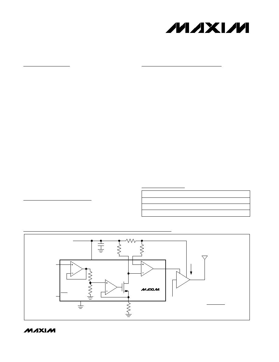
MAX4473
Low-Cost, Low-Voltage, PA Power Control
Amplifier for GSM Applications in 8-Pin QFN
________________________________________________________________ Maxim Integrated Products
1
GND
PC
0.1
µF
8
7
R
3R
A3
PA
GC
IN
RFIN
4
3 SHDN
BUFFER
5
6
A2
Q1
A1
1
2
SR1
SR2
SR3
RG3
OUT
V-TO-I
CONVERTER
ERROR
AMPLIFIER
V
CC
V
CC
V
CC
R
SENSE
RG1
RG2
I
CCPA
MAX4473
4 · RG3 · R
SENSE
V
PC
· RG1
I
CCPA
=
Typical Operating Circuit
19-1448; Rev 3; 8/02
Pin Configuration appears at end of data sheet.
Ordering Information
Rail-to-Rail is a registered trademark of Nippon Motorola, Ltd.
For pricing, delivery, and ordering information, please contact Maxim/Dallas Direct! at
1-888-629-4642, or visit Maxim's website at www.maxim-ic.com.
PART
TEMP RANGE
PIN-PACKAGE
MAX4473EUA
-40°C to +85°C
8 µMAX
MAX4473ETA
-40°C to +85°C
8 QFN
MAX4473ESA
-40°C to +85°C
8 SO
MAX4473
Low-Cost, Low-Voltage, PA Power Control
Amplifier for GSM Applications in 8-Pin QFN
2
_______________________________________________________________________________________
ABSOLUTE MAXIMUM RATINGS
ELECTRICAL CHARACTERISTICS
(V
CC
= 2.7V to 6.5V, SHDN > 2.4V, MAX4473 test circuit, RG1 = RG2 = 1k
±1%, RG3 = 2.5k ±1%, R
SENSE
= 100
±1%,
R
L
= 10k
, C
L
= 300pF, T
A
= T
MIN
to T
MAX
, unless otherwise noted. Typical values are at V
CC
= 6.0V, V
PC
= 1.0V, T
A
= +25°C.) (Note 1)
Stresses beyond those listed under "Absolute Maximum Ratings" may cause permanent damage to the device. These are stress ratings only, and functional
operation of the device at these or any other conditions beyond those indicated in the operational sections of the specifications is not implied. Exposure to
absolute maximum rating conditions for extended periods may affect device reliability.
V
CC
to GND..............................................................................7V
SR1, SR2, SR3, PC, SHDN,
OUT to GND ............................................-0.3V to (V
CC
+ 0.3V)
SR1 to SR3......................................................................0 to V
CC
OUT and SR3 Short-Circuit Duration
to V
CC
or GND ........................................................Continuous
Current into Any Pin..........................................................±50mA
Continuous Power Dissipation (T
A
= +70°C)
8-Pin µMAX (derate 4.10mW/°C above +70°C) ............330mW
8-Pin QFN (derate 24.4mW/°C above +70°C) ............1951mW
8-Pin SO (derate 5.88mW/°C above +70°C).................471mW
Operating Temperature Range ...........................-40°C to +85°C
Junction Temperature. .....................................................+150°C
Storage Temperature Range. ............................-65°C to +150°C
Lead Temperature (soldering, 10s) .................................+300°C
V
OUT
= V
CC
/ 2
R
L
= 500
to V
CC
/ 2
V
PC
= 0
2.7V < V
CC
< 6.5V, V
PC
= GND
1V < V
SR1
, V
SR2
< V
CC
,
V
PC
= GND
Inferred from CMRR test; V
PC
= GND (Note 2)
1V < V
SR1
, V
SR2
< V
CC
SHDN < 0.4V, V
SR1
= V
SR2
= V
CC
1V < V
SR1
, V
SR2
< V
CC
SHDN < 0.4V, R
L
= 10k
1V < V
SR1
, V
SR2
< V
CC
, V
PC
= GND,
SR3 = unconnected
SHDN = 0 to V
CC
1V < V
SR1
, V
SR2
< V
CC
, V
PC
= GND,
SR3 = unconnected
CONDITIONS
mA
20
Output Current Limit
0.15
V
CC
- 0.15
80
120
80
130
80
125
dB
80
130
dB
80
90
Power-Supply Rejection Ratio
75
95
65
85
Common-Mode Rejection Ratio
µA
±0.001
±0.5
SR1, SR2 Shutdown Leakage Current
µA
±0.001
±0.2
SR1, SR2 Input Bias Offset Current
µA
±0.04
±1
SR1, SR2 Input Bias Current
mA
1.2
2
Supply Current
V
2.7
6.5
Supply Voltage
V
1
V
CC
SR1, SR2 Input Common-Mode
Voltage Range
µV/
°C
10
SR1, SR2 Input Offset Voltage Drift
±0.5
±2
µA
0.03
1
Shutdown Supply Current
V
2.4
SHDN Input High Voltage
V
0.4
SHDN Input Low Voltage
µA
±0.5
SHDN Input Current
UNITS
MIN
TYP
MAX
PARAMETER
V
CC
= 2.7V
V
CC
= 6.5V
V
CC
= 6.5V, 0.3V < V
OUT
< 6V
V
CC
= 2.7V, 0.3V < V
OUT
< 2.4V
R
L
= 10k
to V
CC
/ 2
V
CC
= 6.5V, 0.7V < V
OUT
< 5.5V
V
CC
= 2.7V, 0.7V < V
OUT
< 2.2V
R
L
= 10k
, C
L
= 300pF
R
L
= 10k
, C
L
= 300pF, f
o
= 10kHz
degrees
60
Phase Margin
MHz
2
Gain-Bandwidth Product
Measured from 30% to 70% of V
OUT
, R
L
= 10k
,
C
L
= 300pF
V/µs
1.8
Slew Rate
Large-Signal Gain
R
L
= 10k
to V
CC
/ 2
R
L
= 500
to V
CC
/ 2
V
0.5
V
CC
- 0.5
Output Voltage Swing
dB
1V < V
SR1
, V
SR2
< V
CC
at +25
°C
mV
±0.5
±1
SR1, SR2 Input Offset Voltage
GENERAL
ERROR AMPLIFIER
MAX4473
Low-Cost, Low-Voltage, PA Power Control
Amplifier for GSM Applications in 8-Pin QFN
_______________________________________________________________________________________
3
ELECTRICAL CHARACTERISTICS (continued)
(V
CC
= 2.7V to 6.5V, SHDN > 2.4V, MAX4473 test circuit, RG1 = RG2 = 1k
±1%, RG3 = 2.5k ±1%, R
SENSE
= 100
±1%,
R
L
= 10k
, C
L
= 300pF, T
A
= T
MIN
to T
MAX
, unless otherwise noted. Typical values are at V
CC
= 6.0V, V
PC
= 1.0V, T
A
= +25°C.) (Note 1)
Note 1: Limits over temperature are guaranteed by design.
Note 2: No output phase-reversal for input common-mode voltage range from GND to V
CC
. Common-mode range limited by voltage
drop across Q1 and RG3.
Note 3: Guaranteed by design.
Note 4: Error dependent on tolerance of RG1, RG2, and RG3. Specified with 0.1% tolerance resistors.
V
PC
= 2.55V, SR1 = SR2 = V
CC
GND < V
PC
< V
CC
- 0.15V
No sustained oscillations (Note 3)
Measure voltage across RG1, 0.3V < V
PC
< 2.55V (Note 4)
Bandwidth from V
PC
to V
RG1
CONDITIONS
mA
0.750
4
SR3 Output Current Limit
µA
±0.04
±1
pF
0
300
Capacitive-Load Stability
PC Input Bias Current
V/V
0.095
0.1
0.105
V
PC
to V
RG1
Ratio
MHz
2
PC Input Bandwidth
UNITS
MIN
TYP
MAX
PARAMETER
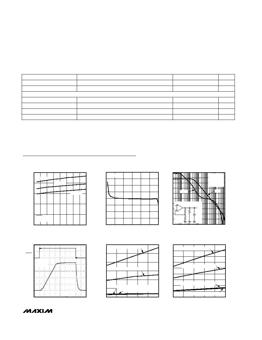
Typical Operating Characteristics
(See Test Circuit, T
A
= +25°C, unless otherwise noted.)
0.4
0.6
1.0
0.8
1.2
1.4
2.5
3.5
4.0
3.0
4.5
5.0
5.5
6.0
6.5
SUPPLY CURRENT vs. SUPPLY VOLTAGE
MAX4473 toc01
SUPPLY VOLTAGE (V)
SUPPLY CURRENT (mA)
T
A
= -40
°C
T
A
= +25
°C
T
A
= +85
°C
SHDN = V
CC
PC = GND
0.0900
0.0925
0.0950
0.0975
0.1000
0.1025
0.1050
0.1075
0.1100
0
2
1
3
4
5
6
V
RG1
/ V
PC
RATIO vs. V
PC
RESPONSE
MAX4473 toc02
V
PC
(V)
V
RG1
/ V
PC
(V/V)
V
CC
= 6.0V
70
0
-30
10
100
1k
10k
100k
1M
10M
ERROR-AMPLIFIER RESPONSE
-10
0
-20
MAX4473 toc03
FREQUENCY (Hz)
GAIN (dB)
PHASE (degrees)
10
20
30
40
50
60
-180
-144
-126
-162
-108
-90
-72
-54
-36
-18
PHASE
GAIN
A
VCL
= 1000
V
CC
= 6.5V
V
CM
= V
CC
/ 2
V
PC
= 0
100k
ERROR
AMPLIFIER
100
10k
300pF
OUT
500mV/div
SHDN
2V/div
ENABLE/DISABLE TIME
MAX4473 toc04
500ns/div
V
CC
= 6.5V
V
PC
= 2V
GND
GND
0
0.10
0.05
0.20
0.15
0.25
0.30
-40
10
-15
35
60
85
ERROR-AMPLIFIER
OUTPUT LOW VOLTAGE vs. TEMPERATURE
MAX4473 toc05
TEMPERATURE (
°C)
V
OL
(V)
V
CC
= 6.5V, R
L
= 10k
to V
CC
/ 2
V
CC
= 2.7V, R
L
= 10k
to V
CC
/ 2
V
CC
= 6.5V, R
L
= 500
to V
CC
/ 2
V
CC
= 2.7V, R
L
= 500
to V
CC
/ 2
0.15
0.10
0.05
0
0.25
0.20
0.35
0.30
0.40
0.45
-40
10
-15
35
60
85
ERROR-AMPLIFIER
OUTPUT HIGH VOLTAGE vs. TEMPERATURE
MAX4473 toc06
TEMPERATURE (
°C)
V
CC
-
V
OH
(V)
V
CC
= 2.7V, R
L
= 10k
to V
CC
/ 2
V
CC
= 6.5V, R
L
= 500
to V
CC
/ 2
V
CC
= 6.5V, R
L
= 10k
to V
CC
/ 2
V
CC
= 2.7V, R
L
= 500
to V
CC
/ 2
From 50% of SHDN edge to V
OUT
= 1V, V
PC
= 2V
µs
0.9
1.5
Enable/Disable Time
GAIN CONTROL BUFFER AND V-TO-I CONVERTER
Detailed Description
The MAX4473 is a voltage-controlled, unidirectional,
high-side current setting amplifier for applications
where accurate control of PA supply current is desired.
This device is intended for wireless TDMA based sys-
tems (GSM, DECT), where tight restrictions over the
PA's transmit burst and output power require closed-
loop control over the PA's output power. When used
with a PA, the MAX4473 functions as a voltage-con-
trolled constant current source, accurately setting PA
supply current by varying the gain of the PA. If you
know the output power versus supply current profile for
the PA, you can set the PA's output power by control-
ling the amount of supply current delivered to the PA.
The MAX4473 is composed of an input buffer (A1), a
voltage-to-current converting amplifier (A2), and a rail-
to-rail output error amplifier (A3) (see Typical Operating
Circuit). External gain and sense resistors allow pro-
grammability for a wide range of applications.
In the Typical Operating Circuit, PA supply current
flows from the system supply, through the external cur-
rent-sense resistor (R
SENSE
), to the PA. The rail-to-rail
outputs of the error amplifier, A3, adjust the gain of the
PA until the voltage drop across R
SENSE
equals the
voltage drop across external gain resistor, RG1. The
voltage drop across RG1 sets the voltage drop across
R
SENSE
, with a larger voltage drop resulting in more
current delivered to the PA. The voltage drop across
RG1 is set by A1, A2, and the V-to-I FET, Q1. A voltage
applied to the PC input of the input buffer is divided by
four by a resistor-divider network. A2 forces its inverting
input and the source of Q1 to V
PC
/ 4, thus setting a
voltage across RG3. The resulting current through RG3
sets the current through RG1. This unique architecture
allows the supply current to be set independent of sup-
ply voltage. Set PA supply current according to the fol-
lowing equation:
I
CCPA
= ( V
PC
· RG1 ) / ( 4 · R
SENSE
· RG3 )
Shutdown Mode
When SHDN is a logic-level low (SHDN < 0.4V), ampli-
fiers A1, A2, and A3 are off, Q1 is turned off, and the
output of A3 is actively pulled to ground with an N-
channel FET. Supply current is reduced to less than
1µA in shutdown mode. Typical power-up time is 0.9µs
and typical power-down time is 0.3µs, using the
MAX4473 test circuit.
Applications Information
Gain Resistor Selection
(RG1, RG2, RG3)
For proper operation, do not make the value of external
gain resistors RG1 and RG2 larger than twice the value
of RG3. In most practical applications, choose RG1
smaller than RG3 to limit the voltage drop over RG1
and R
SENSE
. A large voltage drop over R
SENSE
sub-
stantially reduces the voltage applied to the PA, thus
reducing PA output power. Set RG2 equal to RG1 to
compensate for the input bias currents of A3.
Recommended values for RG3 are between 1k
and
10k
.
MAX4473
Low-Cost, Low-Voltage, PA Power Control
Amplifier for GSM Applications in 8-Pin QFN
4
_______________________________________________________________________________________
NAME
FUNCTION
1
SR1
Inverting Input of Error Amplifier and Drain of V-to-I FET, Q1. Connect to supply side of current-sense resis-
tor, R
SENSE
, through gain resistor RG1.
2
SR2
Noninverting Input of Error Amplifier. Connect to load side of current-sense resistor, R
SENSE
, through gain
resistor RG2. Set RG2 equal to RG1.
PIN
3
SHDN
Shutdown Input. Drive SHDN low to disable all amplifiers, pull OUT to GND, set the gate-to-source voltage
of the V-to-I FET (Q1) to 0, and reduce supply current to less than 1µA. Drive high or connect to V
CC
for nor-
mal operation.
4
PC
Power Control Input. Apply a voltage to PC to set a DC current through the sense resistor to control PA bias.
8
V
CC
+2.7V to +6.5V Voltage Supply Input. Bypass to ground with a 0.1µF capacitor.
7
OUT
Output of Error Amplifier. Connect to gain control pin of power amplifier in bias control applications.
6
SR3
Inverting Input of V-to-I Converter and Source of V-to-I FET, Q1. Connect to ground through gain resistor
RG3.
5
GND
Ground
Pin Description
Sense Resistor Selection (R
SENSE
)
Choose R
SENSE
based on the following criteria:
· Voltage Loss: A high R
SENSE
value causes the
power-source voltage to degrade through IR loss.
For minimal voltage loss, use low R
SENSE
values.
· Accuracy: A high R
SENSE
value allows lower cur-
rents to be measured more accurately because input
offset voltages become less significant when the
sense voltage is larger. For best performance, select
R
SENSE
to provide approximately 100mV of sense
voltage for the full-scale current in each application.
· Efficiency and Power Dissipation: At high current
levels, the I
2
R losses in R
SENSE
are significant. Take
this into consideration when choosing the resistor
value and its power dissipation (wattage) rating.
Also, the sense resistor's value may drift if it is
allowed to heat up excessively.
MAX4473
Low-Cost, Low-Voltage, PA Power Control
Amplifier for GSM Applications in 8-Pin QFN
_______________________________________________________________________________________
5
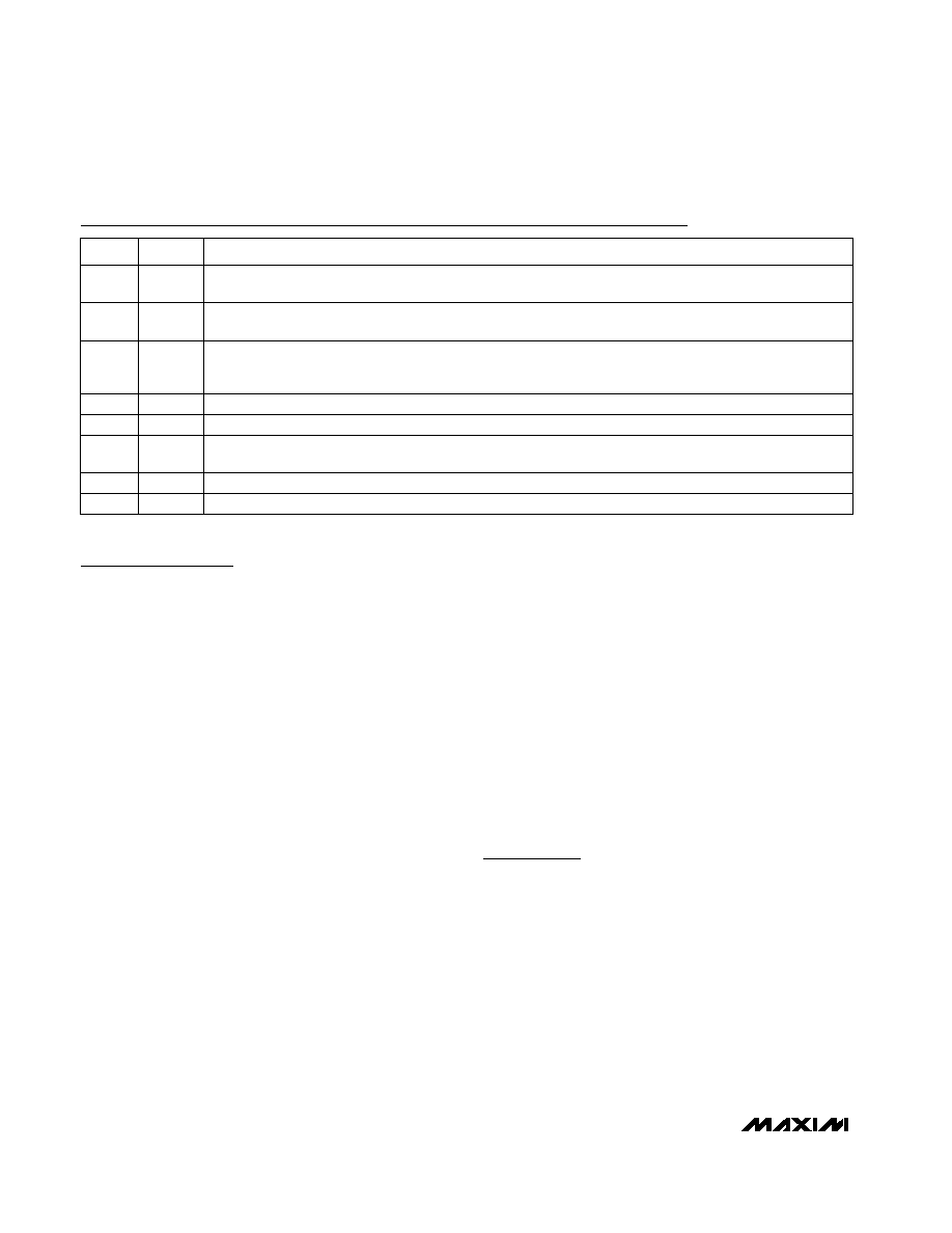
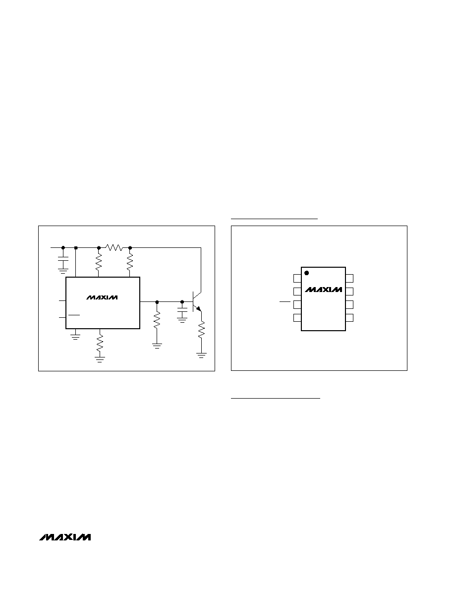
_________________________Test Circuit
2N3904
SR1
GND
R
SENSE
SR2
OUT
SR3
PC
SHDN
V
CC
V
CC
C
L
300pF
R
L
10k
RG1
1k
1%
RG2
1k
1%
RG3
2.5k
1%
100
0.1%
0.1
µF
MAX4473
R
E
750
Pin Configuration
SR3
GND
PC
1
2
8
7
V
CC
OUT
SR2
SR1
QFN/
µMAX/SO
TOP VIEW
3
4
6
5
MAX4473
SHDN
Chip Information
TRANSISTOR COUNT: 348