 | ÐлекÑÑоннÑй компоненÑ: MAX4608 | СкаÑаÑÑ:  PDF PDF  ZIP ZIP |
Äîêóìåíòàöèÿ è îïèñàíèÿ www.docs.chipfind.ru
General Description
The MAX4607/MAX4608/MAX4609 dual analog switches
feature low on-resistance of 2.5
max. On-resistance is
matched between switches to 0.5
max and is flat (0.5
max) over the specified signal range. Each switch can
handle Rail-to-Rail
®
analog signals. The off-leakage cur-
rent is only 2.5nA max at +85°C. These analog switches
are ideal in low-distortion applications and are the pre-
ferred solution over mechanical relays in automatic test
equipment or applications where current switching is
required. They have low power requirements, require
less board space, and are more reliable than mechani-
cal relays.
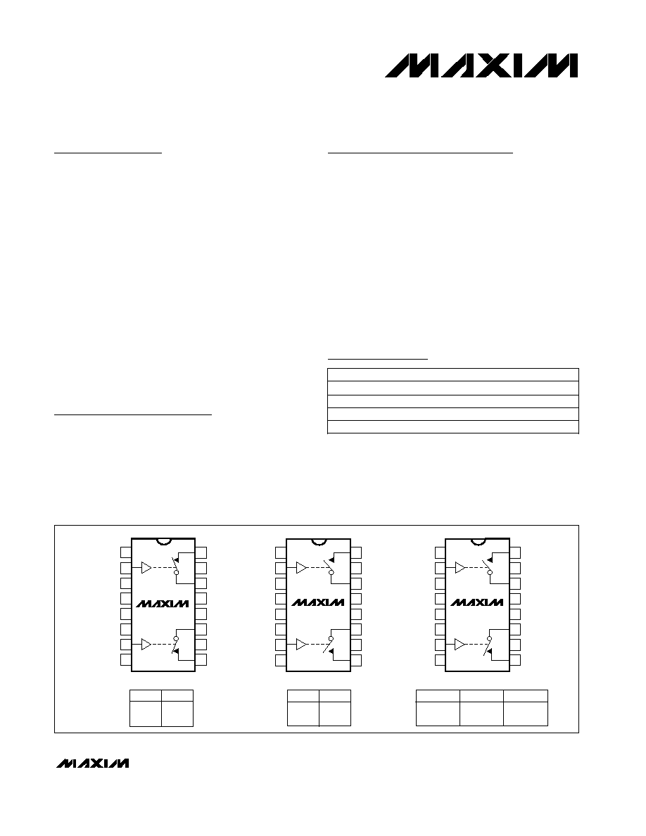
The MAX4607 has two normally closed (NC) switches,
the MAX4608 has two normally open (NO) switches,
and the MAX4609 has one NC and one NO switch.
These switches operate from a single supply of +4.5V to
+36V or from dual supplies of ±4.5V to ±20V. All digital
inputs have +0.8V and +2.4V logic thresholds, ensuring
TTL/CMOS-logic compatibility when using dual ±15V or
a single +12V supply.
Applications
Reed Relay Replacement
PBX, PABX Systems
Test Equipment
Audio-Signal Routing
Communication Systems
Avionics
Features
o
Low On-Resistance (2.5
max)
o
Guaranteed R
ON
Match Between Channels
(0.5
max)
o
Guaranteed R
ON
Flatness over Specified Signal
Range (0.5
max)
o
Rail-to-Rail Signal Handling
o
Guaranteed ESD Protection > 2kV
per Method 3015.7
o
Single-Supply Operation: +4.5V to +36V
Dual-Supply Operation: ±4.5V to ±20V
o
TTL/CMOS-Compatible Control Inputs
MAX4607/MAX4608/MAX4609
2.5
, Dual, SPST,
CMOS Analog Switches
________________________________________________________________
Maxim Integrated Products
1
SO/DIP
TOP VIEW
SO/DIP
LOGIC
SWITCH
0
1
ON
OFF
LOGIC
SWITCH
0
1
OFF
ON
SO/DIP
LOGIC
SWITCH 1
0
1
OFF
ON
SWITCH 2
ON
OFF
16
15
14
13
12
11
10
9
1
2
3
4
5
6
7
8
NO1
N.C.
COM1
V+
V-
N.C.
IN1
N.C.
MAX4609
V
L
COM2
N.C.
NC2
N.C.
IN2
N.C.
GND
16
15
14
13
12
11
10
9
1
2
3
4
5
6
7
8
NC1
N.C.
COM1
V+
V-
N.C.
IN1
N.C.
MAX4607
V
L
COM2
N.C.
NC2
N.C.
IN2
N.C.
GND
16
15
14
13
12
11
10
9
1
2
3
4
5
6
7
8
NO1
N.C.
COM1
V+
V-
N.C.
IN1
N.C.
MAX4608
V
L
COM2
N.C.
NO2
N.C.
IN2
N.C.
GND
19-1392; Rev 1; 8/99
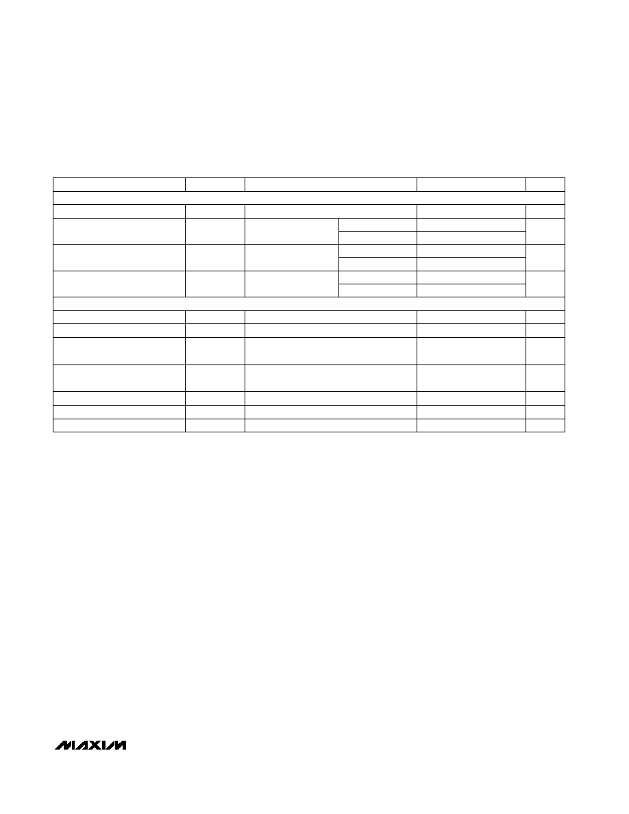
PART
MAX4607
CSE
MAX4607CPE
0°C to +70°C
0°C to +70°C
TEMP. RANGE
PIN-PACKAGE
16 Narrow SO
16 Plastic DIP
Ordering Information continued at end of data sheet.
______________________ Pin Configurations/Functional Diagrams/Truth Tables
Ordering Information
Rail-to-Rail is a registered trademark of Nippon Motorola, Ltd.
MAX4607ESE
-40°C to +85°C
16 Narrow SO
MAX4607EPE
-40°C to +85°C
16 Plastic DIP
For free samples & the latest literature: http://www.maxim-ic.com, or phone 1-800-998-8800.
For small orders, phone 1-800-835-8769.
MAX4607/MAX4608/MAX4609
2.5
, Dual, SPST,
CMOS Analog Switches
2
_______________________________________________________________________________________
ABSOLUTE MAXIMUM RATINGS
ELECTRICAL CHARACTERISTICS--Dual Supplies
(V+ = +15V, V- = -15V, V
L
= +5V, V
IN_H
= +2.4V, V
IN_L
= +0.8V, T
A
= T
MIN
to T
MAX
, unless otherwise noted. Typical values are at
T
A
= +25°C.) (Note 2)
Stresses beyond those listed under "Absolute Maximum Ratings" may cause permanent damage to the device. These are stress ratings only, and functional
operation of the device at these or any other conditions beyond those indicated in the operational sections of the specifications is not implied. Exposure to
absolute maximum rating conditions for extended periods may affect device reliability.
V+ to GND ..............................................................-0.3V to +44V
V- to GND ...............................................................+0.3V to -44V
V+ to V-...................................................................-0.3V to +44V
V
L
to GND ........................................(GND - 0.3V) to (V+ + 0.3V)
All Other Pins to GND (Note 1) .............(V- - 0.3V) to (V+ + 0.3V)
Continuous Current (COM_, NO_, NC_).........................±100mA
Peak Current (COM_, NO_, NC_)
(pulsed at 1ms, 10% duty cycle)................................ ±300mA
Continuous Power Dissipation (T
A
= +70°C)
Narrow SO (derate 8.70mW/°C above +70°C) .............696mW
Plastic DIP (derate 10.53mW/°C above +70°C) ...........842mW
Operating Temperature Ranges
MAX460_C_E ......................................................0°C to +70°C
MAX460_E_E ...................................................-40°C to +85 °C
Storage Temperature Range .............................-65°C to +160°C
Lead Temperature (soldering, 10sec) .............................+300°C
-2.5
2.5
-2.5
2.5
-10
10
T
A
= T
MIN
to T
MAX
V
T
A
= +25°C
V-
V+
V
COM_,
V
NO_,
V
NC_
Input Voltage Range
(Note 3)
IN_ = 0.8V, all others = 2.4V
IN_ = 2.4V, all others = 0.8V
I
COM_
= 10mA,
V
NO_
or V
NC_
= ±10V
T
A
= +25°C
T
A
= +25°C
T
A
= +25°C
CONDITIONS
1.7
0.8
V
IN_L
Logic Input Low Voltage
0.05
0.4
R
ON
COM_ to NO_, COM_ to NC_
On-Resistance Match Between
Channels (Note 4)
1.6
2.5
R
ON
COM_ to NO_, COM_ to NC_
On-Resistance
V
2.4
1.7
V
IN_H
Logic Input High Voltage
-0.500
0.001
0.500
I
IN_L
Input Current with Input Voltage
Low
µA
-0.500
0.001
0.500
I
IN_H
Input Current with Input Voltage
High
0.1
0.4
R
FLAT(ON)
COM_ to NO_, COM_ to NC_
On-Resistance Flatness (Note 5)
nA
-0.5
0.01
0.5
I
NO_,
I
NC_
Off-Leakage Current
(NO_ or NC_) (Note 6)
nA
-0.5
0.01
0.5
I
COM_(OFF)
COM Off-Leakage Current
(Note 6)
nA
-1
0.02
1
I
COM_(ON)
COM On-Leakage Current
(Note 6)
UNITS
MIN
TYP
MAX
SYMBOL
PARAMETER
I
COM_
= 10mA, V
NO_
or V
NC_
= -5V, 0, 5V
I
COM_
= 10mA,
V
NO_
or V
NC_
= ±10V
T
A
= +25°C
V
COM_
= ±10V,
V
NO_
or V
NC_
=
+
10V
V
COM_
= ±10V,
V
NO_
or V
NC_
=
+
10V
V
COM_
= ±10V,
V
NO_
or V
NC_
= ±10V,
or floating
T
A
= +25°C
T
A
= T
MIN
to T
MAX
3
0.5
T
A
= T
MIN
to T
MAX
0.5
T
A
= T
MIN
to T
MAX
T
A
= T
MIN
to T
MAX
T
A
= T
MIN
to T
MAX
µA
V
Note 1:
Signals on NC_, NO_, COM_, or IN_, exceeding V+ or V- will be clamped by internal diodes. Limit forward diode current to max-
imum current rating.
ANALOG SWITCH
LOGIC INPUT
MAX4607/MAX4608/MAX4609
2.5
, Dual, SPST,
CMOS Analog Switches
_______________________________________________________________________________________
3
T
A
= T
MIN
to T
MAX
V
IN
= 0 or 5V
T
A
= +25°C
-0.5
0.001
0.5
I+
Positive Supply Current
T
A
= +25°C
f = 1MHz, Figure 6, T
A
= +25°C
R
L
= 50
, C
L
= 5pF, f = 1MHz, Figure 5,
T
A
= +25°C
T
A
= T
MIN
to T
MAX
5
5
R
L
= 50
, C
L
= 5pF, f = 1MHz, Figure 4,
T
A
= +25°C
C
L
= 1.0nF, V
GEN
= 0, R
GEN
= 0,
Figure 3, T
A
= +25°C
V
IN
= 0 or 5V
T
A
= +25°C
f = 1MHz, Figure 6, T
A
= +25°C
CONDITIONS
V
±4.5
±20.0
Power-Supply Range
pF
dB
f = 1MHz, Figure 7, T
A
= +25°C
pF
290
C
COM
On-Capacitance
65
C
COM
COM_ Off-Capacitance
-0.5
0.001
0.5
I
L
Logic Supply Current
-0.5
0.001
0.5
I-
Negative Supply Current
pF
65
C
OFF
NC_ or NO_ Capacitance
-66
V
CT
Crosstalk (Note 8)
dB
-60
V
ISO
Off-Isolation (Note 7)
pC
450
Q
Charge Injection
-0.5
0.001
0.5
I
GND
Ground Current
ns
110
t
ON
Turn-On Time
ns
150
t
OFF
Turn-Off Time
UNITS
MIN
TYP
MAX
SYMBOL
PARAMETER
V
IN
= 0 or 5V
V
IN
= 0 or 5V
T
A
= +25°C
V
COM_
= ±10V, Figure 2, T
A
= +25°C
V
COM_
= ±10V, Figure 2, T
A
= +25°C
T
A
= T
MIN
to T
MAX
5
5
5
5
T
A
= T
MIN
to T
MAX
5
5
ELECTRICAL CHARACTERISTICS--Dual Supplies (continued)
(V+ = +15V, V- = -15V, V
L
= +5V, V
IN_H
= +2.4V, V
IN_L
= +0.8V, T
A
= T
MIN
to T
MAX
, unless otherwise noted. Typical values are at
T
A
= +25°C.) (Note 2)
µA
µA
µA
µA
POWER SUPPLY
SWITCH DYNAMIC CHARACTERISTICS
MAX4607/MAX4608/MAX4609
2.5
, Dual, SPST,
CMOS Analog Switches
4
_______________________________________________________________________________________
ELECTRICAL CHARACTERISTICS--Single Supply
(V+ = +12V, V- = 0, V
L
= +5V, V
IN_H
= +2.4V, V
IN_L
= +0.8V, T
A
= T
MIN
to T
MAX
, unless otherwise noted. Typical values are at
T
A
= +25°C.) (Note 2)
-2.5
2.5
-2.5
2.5
-10
10
T
A
= T
MIN
to T
MAX
V
T
A
= +25°C
GND
V+
V
COM_,
V
NO_,
V
NC_
Input Voltage Range
(Note 3)
µA
IN_ = 0.8V, all others = 2.4V
V
IN_ = 2.4V, all others = 0.8V
I
COM_
= 10mA,
V
NO_
or V
NC_
= 10V
T
A
= +25°C
T
A
= +25°C
T
A
= +25°C
CONDITIONS
1.7
0.8
V
IN_L
Logic Input Low Voltage
0.05
0.4
R
ON
COM_ to NO_, COM_ to NC_
On-Resistance Match Between
Channels (Note 4)
3
6
R
ON
COM_ to NO_, COM_ to NC_
On-Resistance
V
2.4
1.7
V
IN_H
Logic Input High Voltage
-0.500
0.001
0.500
I
IN_L
Input Current with
Input Voltage Low
µA
-0.500
0.001
0.500
I
IN_H
Input Current with
Input Voltage High
0.05
0.5
R
FLAT(ON)
COM_ to NO_, COM_ to NC_
On-Resistance Flatness
(Note 5)
nA
-0.5
0.01
0.5
I
NO_
I
NC_
Off-Leakage Current
(NO_ or NC_) (Notes 6, 9)
nA
-0.5
0.01
0.5
I
COM_(OFF)
COM Off-Leakage Current
(Notes 6, 9)
nA
-1
0.01
1
I
COM_(ON)
COM On-Leakage Current
(Notes 6, 9)
UNITS
MIN
TYP
MAX
SYMBOL
PARAMETER
I
COM_
= 10mA,
V
NO_
or V
NC_
= 10V
I
COM_
= 10mA,
V
NO_
or V
NC_
= 3V,
6V, 0V
T
A
= +25°C
V
COM_
= 1V, 10V,
V
NO_
or V
NC_
= 1V,
10V
V
COM_
= 10V, 1V
V
NO_
or V
NC_
= 1V,
10V
V
COM_
= 1V, 10V,
V
NO_
or V
NC_
= 1V,
10V, or floating
T
A
= +25°C
T
A
= T
MIN
to T
MAX
7
0.5
T
A
= T
MIN
to T
MAX
0.5
T
A
= T
MIN
to T
MAX
T
A
= T
MIN
to T
MAX
T
A
= T
MIN
to T
MAX
ANALOG SWITCH
LOGIC INPUT
MAX4607/MAX4608/MAX4609
2.5
, Dual, SPST,
CMOS Analog Switches
_______________________________________________________________________________________
5
Note 2:
The algebraic convention, where the most negative value is a minimum and the most positive value a maximum, is used in
this data sheet.
Note 3:
Guaranteed by design.
Note 4:
R
ON
= R
ON(MAX)
- R
ON(MIN)
Note 5:
Flatness is defined as the difference between the maximum and minimum value of on-resistance as measured over the
specified analog signal range.
Note 6:
Leakage parameters are 100% tested at maximum-rated hot temperature and guaranteed by correlation at +25°C.
Note 7:
Off-isolation = 20log
10
[V
COM
/ (V
NC
or V
NO
)], V
COM
= output, V
NC
or V
NO
= input to off switch.
Note 8:
Between any two switches.
Note 9:
Leakage testing at single supply is guaranteed by testing with dual supplies.
ELECTRICAL CHARACTERISTICS--Single Supply (continued)
(V+ = +12V, V- = 0, V
L
= +5V, V
IN_H
= +2.4V, V
IN_L
= +0.8V, T
A
= T
MIN
to T
MAX
, unless otherwise noted. Typical values are at
T
A
= +25°C.) (Note 2)
V
IN
= 0 or 5V
T
A
= +25°C
-0.5
0.001
0.5
I+
Positive Supply Current
T
A
= +25°C
f = 1MHz, Figure 6, T
A
= +25°C
R
L
= 50
, C
L
= 5pF, f = 1MHz, Figure 5,
T
A
= +25°C
T
A
= T
MIN
to T
MAX
5
5
C
L
= 1.0nF, V
GEN
= 0, R
GEN
= 0, Figure 3,
T
A
= +25°C
T
A
= +25°C
f = 1MHz, Figure 6, T
A
= +25°C
CONDITIONS
V
+4.5
+36.0
Power-Supply Range
pF
dB
f = 1MHz, Figure 7, T
A
= +25°C
pF
185
C
(COM)
On-Capacitance
µA
µA
µA
105
C
(COM)
COM Off-Capacitance
-0.5
0.001
0.5
I
L
Logic Supply Current
pF
105
C
(OFF)
NC or NO Capacitance
66
V
CT
Crosstalk (Note 8)
pC
50
Q
Charge Injection
-0.5
0.001
0.5
I
GND
Ground Current
ns
110
t
ON
Turn-On Time
ns
130
t
OFF
Turn-Off Time
UNITS
MIN
TYP
MAX
SYMBOL
PARAMETER
V
IN
= 0 or 5V
V
IN
= 0 or 5V
V
COM_
= 10V, Figure 2, T
A
= +25°C
V
COM_
= 10V, Figure 2, T
A
= +25°C
T
A
= T
MIN
to T
MAX
5
5
T
A
= T
MIN
to T
MAX
5
5
POWER SUPPLY
SWITCH DYNAMIC CHARACTERISTICS