 | –≠–ª–µ–∫—Ç—Ä–æ–Ω–Ω—ã–π –∫–æ–º–ø–æ–Ω–µ–Ω—Ç: MAX4644 | –°–∫–∞—á–∞—Ç—å:  PDF PDF  ZIP ZIP |

General Description
The MAX4644 is a single-pole/double-throw (SPDT)
switch that operates from a single supply ranging from
+1.8V to +5.5V. It provides low 4
on-resistance (R
ON
)
as well as 1
R
ON
flatness over the entire analog signal
range. The MAX4644 offers fast switching times of less
than 20ns while ensuring break-before-make operation.
It typically consumes only 0.01µW of quiescent power,
making it suitable for use in low-power, portable appli-
cations.
The MAX4644's features include low leakage currents
over the entire temperature range, TTL/CMOS-compati-
ble digital logic, and excellent AC characteristics. It is
packaged in either a small 8-pin µMAX or a tiny 6-pin
SOT23.
________________________Applications
Battery-Operated Equipment
Audio and Video Signal Routing
Low-Voltage Data-Acquisition Systems
Sample-and-Hold Circuits
Communications Circuits
Features
o +1.8V to +5.5V Single-Supply Operation
o Rail-to-Rail
Æ
Analog Signal Range
o Guaranteed R
ON
4
max (+5V supply)
8
max (+3V supply)
o +1.8V Operation
R
ON
30
typ Over Temperature
t
ON
18ns typ, t
OFF
12ns typ
o Guaranteed R
ON
Flatness: 0.75
typ (+5V supply)
o Guaranteed R
ON
Match Between Channels:
0.1
typ (+5V supply)
o Low Leakage (<0.35nA) Over Entire Temperature
Range
o Excellent AC Characteristics
Low Crosstalk: -82dB at 1MHz
High Off-Isolation: -80dB at 1MHz
0.018% Total Harmonic Distortion
o Low Power Consumption: < 0.01µW
MAX4644
High-Speed, Low-Voltage, 4
,
SPDT CMOS Analog Switch
________________________________________________________________ Maxim Integrated Products
1
NC
GND
1
2
6
5
NO
COM
V+
IN
3
4
MAX4644
SOT23-6
MAX4644
IN
GND
N.C.
V+
1
2
8
7
NO
N.C.
NC
COM
3
4
6
5
µMAX
TOP VIEW
IN
0
1
NC
NO
MAX4644
OFF
ON
ON
OFF
Pin Configurations/Functional Diagrams/Truth Table
19-1657; Rev 0; 3/00
For free samples and the latest literature, visit www.maxim-ic.com or phone 1-800-998-8800.
For small orders, phone 1-800-835-8769.
Ordering Information
PIN-
PACKAGE
TEMP. RANGE
PART
8 µMAX
-40∞C to +85∞C
MAX4644EUA
6 SOT23-6
-40∞C to +85∞C
MAX4644EUT-T
TOP
MARK
--
AAHQ
Rail-to-Rail is a trademark of Nippon Motorola, Ltd.
MAX4644
High-Speed, Low-Voltage, 4
,
SPDT CMOS Analog Switch
2
_______________________________________________________________________________________
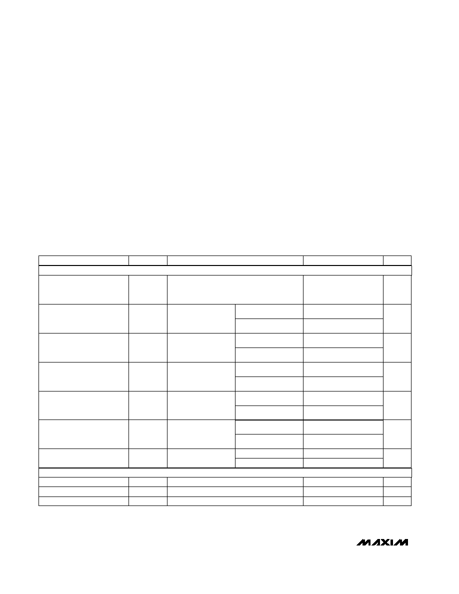
ELECTRICAL CHARACTERISTICS--Single +5V Supply
(V+ = +4.5V to +5.5V, V
INH
= 2.4V, V
INL
= 0.8V, T
A
= T
MIN
to T
MAX
, unless otherwise noted. Typical values are at T
A
= +25∞C.)
Stresses beyond those listed under "Absolute Maximum Ratings" may cause permanent damage to the device. These are stress ratings only, and functional
operation of the device at these or any other conditions beyond those indicated in the operational sections of the specifications is not implied. Exposure to
absolute maximum rating conditions for extended periods may affect device reliability.
All Voltages Referenced to GND
V+ .............................................................................-0.3V to +6V
IN, COM, NO, NC (Note 1) ...........................-0.3V to (V+ + 0.3V)
Continuous Current (any terminal)....................................±20mA
Continuous Current (NO, NC, and COM) .........................±50mA
Peak Current (NO, NC, and COM, pulsed at 1ms,
10% duty cycle)......................................................... ±100mA
Continuous Power Dissipation (T
A
= +70∞C)
6-Pin SOT23 (derate 8.70mW/∞C above +70∞C)........ 696mW
8-Pin µMAX (derate 4.5mW/∞C above +70∞C) ........... 362mW
Operating Temperature Range ...........................-40∞C to +85∞C
Junction Temperature ......................................................+150∞C
Storage Temperature Range .............................-65∞C to +150∞C
Lead Temperature (soldering, 10s) ................................ +300∞C
V+ = 4.5V, I
COM
=
10mA, V
NO
or
V
NC
= 0 to V+
V
IN
= 0.8V or 2.4V
V+ = 5.5V, V
COM
=
1V or 4.5V
V+ = 4.5V, I
COM
=
10mA, V
NO
or
V
NC
= 0 to V+
V+ = 4.5V, I
COM
=
10mA, V
NO
or
V
NC
= 0 to V+
CONDITIONS
µA
-0.1
0.005
0.1
I
IN
Input Current
V
0.8
V
IL
Input Logic Low
V
2.4
V
IH
Input Logic High
2.5
4
R
ON
On-Resistance
V
0
V+
V
COM
,
V
NO
,
V
NC
Analog Signal Range
DIGITAL INPUTS
-0.35
0.35
I
COM(ON)
nA
-0.25
0.01
0.25
COM On-Leakage Current
(Notes 4, 5)
1.2
4.75
0.1
R
ON
On-Resistance Match
Between Channels (Note 2)
0.4
0.75
1
R
FLAT
On-Resistance Flatness
(Note 3)
UNITS
MIN
TYP
MAX
SYMBOL
PARAMETER
Note 1: Signals on NO, NC, COM, or IN exceeding V+ or GND are clamped by internal diodes. Limit forward-diode current to maximum
current rating.
T
A
= +25∞C
T
A
= T
MIN
to T
MAX
T
A
= +25∞C
T
A
= T
MIN
to T
MAX
T
A
= +25∞C
T
A
= T
MIN
to T
MAX
T
A
= +25∞C
V+ = 5.5V, V
COM
=
1V or 4.5V, V
NO
or
V
NC
= 4.5V or 1V
-0.35
0.35
T
A
= T
MIN
to T
MAX
nA
-0.25
0.01
0.25
I
NO(OFF)
,
I
NC(OFF)
NO, NC Off-Leakage
Current (Note 4)
T
A
= +25∞C
V+ = 5.5V, V
COM
=
1V or 4.5V, V
NO
or
V
NC
= 4.5V or 1V
-0.35
0.35
T
A
= T
MIN
to T
MAX
nA
-0.25
0.01
0.25
I
COM(OFF)
COM Off-Leakage Current
(Note 4)
T
A
= +25∞C
T
A
= T
MIN
to T
MAX
ANALOG SWITCH
DIGITAL INPUTS
ABSOLUTE MAXIMUM RATINGS

MAX4644
High-Speed, Low-Voltage, 4
,
SPDT CMOS Analog Switch
_______________________________________________________________________________________
3
ELECTRICAL CHARACTERISTICS --Single +5V Supply (continued)
(V+ = +4.5V to +5.5V, V
INH
= 2.4V, V
INL
= 0.8V, T
A
= T
MIN
to T
MAX
, unless otherwise noted. Typical values are at T
A
= +25∞C.)
ELECTRICAL CHARACTERISTICS--Single +3V Supply
(V+ = +2.7V to +3.3V, V
INH
= 2.0V, V
INL
= 0.4V, T
A
= T
MIN
to T
MAX
, unless otherwise noted. Typical values are at T
A
= +25∞C.)
R
L
= 300
; C
L
=
35pF; V
NO
, V
NC
= 3V;
Figure 2
R
L
= 600
, 0.5Vp-p, f = 20Hz to 20kHz
C
L
= 5pF, R
L
= 50
,
Figure 3
f = 1MHz, Figure 5
T
A
= +25∞C
R
L
= 300
; C
L
=
35pF; V
NO
, V
NC
= 3V;
Figure 2
T
A
= +25∞C
NO or NC = GND, f = 1MHz, Figure 5
R
L
= 300
;
C
L
= 35pF; V
NO
or
V
NC
= +3V; Figure 2
V
GEN
= 0, R
GEN
= 0, C
L
= 1nF, Figure 4
CONDITIONS
%
0.018
THD
Total Harmonic Distortion
dB
-80
V
ISO
Off-Isolation (Note 6)
pF
34
C
(ON)
Switch On-Capacitance
pF
12
C
NO(OFF),
C
NC(OFF)
NO, NC Off-Capacitance
pC
5
Q
Charge Injection
ns
11
15
t
ON
Turn-On Time (Note 4)
1
T
A
= T
MIN
to T
MAX
18
T
A
= +25∞C
T
A
= T
MIN
to T
MAX
ns
3
5
t
OFF
Turn-Off Time (Note 4)
6
T
A
= T
MIN
to T
MAX
ns
8
t
BBM
Break-Before-Make (Note 4)
UNITS
MIN
TYP
MAX
SYMBOL
PARAMETER
V+ = 5.5V, V
IN
= 0 or V+
µA
0.001
1.0
I+
Positive Supply Current
f = 1MHz
f = 10MHz
C
L
= 5pF, R
L
= 50
,
Figure 3
f = 1MHz
f = 10MHz
dB
-82
V
CT
Crosstalk (Note 7)
-55
-62
V+ = 2.7V, I
COM
=
10mA, V
NO
or
V
NC
= 0 to V+
T
A
= +25∞C
V+ = 2.7V, I
COM
=
10mA, V
NO
or
V
NC
= 0 to V+
V+ = 2.7V, I
COM
=
10mA, V
NO
or
V
NC
= 0 to V+
CONDITIONS
6
8
R
ON
On-Resistance
V
0
V+
V
COM
,
V
NO
,
V
NC
Analog Signal Range
T
A
= T
MIN
to T
MAX
9
T
A
= +25∞C
T
A
= T
MIN
to T
MAX
0.1
R
ON
On-Resistance Match
Between Channels (Note 2)
0.4
T
A
= +25∞C
1.5
3
R
FLAT
On-Resistance Flatness
(Note 3)
UNITS
MIN
TYP
MAX
SYMBOL
PARAMETER
DYNAMIC
SUPPLY
T
A
= T
MIN
to T
MAX
3.5
ANALOG SWITCH

MAX4644
High-Speed, Low-Voltage, 4
,
SPDT CMOS Analog Switch
4
_______________________________________________________________________________________
ELECTRICAL CHARACTERISTICS--Single +3V Supply (continued)
(V+ = +2.7V to +3.3V, V
INH
= 2.0V, V
INL
= 0.4V, T
A
= T
MIN
to T
MAX
, unless otherwise noted. Typical values are at T
A
= +25∞C.)
Note 2:
R
ON
= R
ON(MAX)
- R
ON(MIN)
.
Note 3: R
ON
flatness is defined as the difference between the maximum and minimum value of on-resistance as measured over the
specified analog signal range.
Note 4: Guaranteed by design.
Note 5: On-Leakage performed with voltage applied to COM, with NO and NC left floating.
Note 6: Off-Isolation = 20log
10
(V
O
/ V
I
), where V
O
is V
COM
and V
I
is either V
NC
or V
NO
from the network analyzer.
Note 7: Crosstalk is measured between the two switches.
NO or NC = GND, f = 1MHz, Figure 5
C
L
= 5pF, R
L
= 50
,
Figure 3
V
GEN
= 0, R
GEN
= 0, C
L
= 1nF, Figure 4
V
IN
= 0.4V or 2.0V
R
L
= 300
; C
L
=
35pF; V
NO
, V
NC
= 2V;
Figure 2
C
L
= 5pF, R
L
= 50
,
Figure 3
R
L
= 300
; C
L
=
35pF; V
NO
, V
NC
= 2V;
Figure 2
CONDITIONS
dB
-62
-80
V
ISO
Off-Isolation (Note 6)
dB
-55
V
0.4
V
IL
Input Logic Low
V
2.0
V
IH
Input Logic High
pF
12
C
NO(OFF)
,
C
NC(OFF)
NO, NC Off-Capacitance
pC
5
Q
Charge Injection
µA
-0.1
0.005
0.1
I
IN
Input Current
ns
22
t
ON
Turn-On Time (Note 4)
ns
8
t
BBM
UNITS
MIN
TYP
MAX
SYMBOL
PARAMETER
14
20
T
A
= T
MIN
to T
MAX
T
A
= +25∞C
R
L
= 300
; C
L
=
35pF; V
NO
, V
NC
= 2V;
Figure 2
ns
8
t
OFF
Turn-Off Time (Note 4)
4
7.5
T
A
= T
MIN
to T
MAX
T
A
= +25∞C
Break-Before-Make (Note 4)
T
A
= +25∞C
T
A
= T
MIN
to T
MAX
1
f = 1MHz, Figure 5
pF
34
C
(ON)
Switch On-Capacitance
-82
V
CT
Crosstalk (Note 7)
f = 10MHz
f = 1MHz
f = 10MHz
f = 1MHz
V+ = 3.3V, V
IN
= 0 or V+
µA
0.001
1.0
I+
Positive Supply Current
DIGITAL INPUTS
DYNAMIC
SUPPLY

MAX4644
High-Speed, Low-Voltage, 4
,
SPDT CMOS Analog Switch
_______________________________________________________________________________________
5
140
120
100
80
60
40
20
0
0
2
1
3
4
5
CHARGE INJECTION vs. V
COM
MAX4644-04
V
COM
(V)
CHARGE INJECTION (pC)
V+ = 5V
I
COM
= 10mA
20
15
10
5
0
0
2
1
3
4
5
ON-RESISTANCE vs. V
COM
MAX4644-01
V
COM
(V)
R
ON
(
)
V+ = 3V
V+ = 2.5V
V+ = 5V
V+ = 1.8V
R
ON
(
)
5
4
3
2
1
-40
10
-15
35
60
85
ON-RESISTANCE vs. TEMPERATURE
MAX4644-02
TEMPERATURE (∞C)
V+ = 3V
V+ = 5V
I
COM
= 10mA
1
-40
85
35
60
-15
10
ON-/OFF-LEAKAGE CURRENT
vs. TEMPERATURE
1000
10
100
MAX4644-03
TEMPERATURE (∞C)
LEAKAGE (pA)
OFF-LEAKAGE
ON-LEAKAGE
0
40
20
80
60
120
100
140
SUPPLY CURRENT vs. SUPPLY VOLTAGE
MAX4644-05
SUPPLY VOLTAGE (V)
SUPPLY CURRENT (nA)
1.8
2.8
3.8
4.8
5.8
IN = GND
IN = V+
300
250
200
150
100
50
0
-40
10
-15
35
60
85
SUPPLY CURRENT vs.
TEMPERATURE
MAX4644-06
TEMPERATURE (∞C)
SUPPLY CURRENT (nA)
IN = GND
V+ = 5V
V+ = 3V
V+ = 1.8V
2.0
1.5
1.0
0.5
0
1.8
3.4
2.6
4.2
5.0
5.8
LOGIC THRESHOLD vs.
SUPPLY VOLTAGE
MAX4644-07
SUPPLY VOLTAGE (V)
LOGIC THRESHOLD (V)
0
3
9
6
12
15
SWITCHING TIMES vs. SUPPLY VOLTAGE
MAX4644-08
SUPPLY VOLTAGE (V)
SWITCHING TIMES (ns)
2
4
3
5
t
OFF
t
ON
0
2
6
4
8
10
SWITCHING TIMES vs. TEMPERATURE
MAX4644-09
TEMPERATURE (∞C)
SWITCHING TIMES (ns)
-40
35
60
10
-15
85
V+ = 5V
t
OFF
t
ON
Typical Operating Characteristics
(V+ = +5V or +3V, V
INH
= V+, V
INL
= GND, T
A
= +25∞C, unless otherwise noted.)