 | –≠–ª–µ–∫—Ç—Ä–æ–Ω–Ω—ã–π –∫–æ–º–ø–æ–Ω–µ–Ω—Ç: MAX4687 | –°–∫–∞—á–∞—Ç—å:  PDF PDF  ZIP ZIP |
General Description
The MAX4686/MAX4687/MAX4688 low on-resistance
(R
ON
), low-voltage analog switches operate from a sin-
gle +1.8V to +5.5V supply. The MAX4686/MAX4687 are
single-pole/single-throw (SPST) analog switches, and
the MAX4688 is a single-pole/double-throw (SPDT) ana-
log switch. The MAX4686 is a normally open (NO)
switch, and the MAX4687 is a normally closed (NC)
switch. The MAX4688 has one normally open (NO)
switch and one normally closed (NC) switch.
When powered from a 3V supply these devices feature
2.5
(max) R
ON
, with 0.4
(max) R
ON
matching and 1
(max) flatness. The MAX4686/MAX4687/MAX4688 offer
fast switching speeds (t
ON
= 30ns max, t
OFF
= 12ns
max). The MAX4688 offers break-before-make action.
The digital logic inputs are 1.8V logic compatible from a
+2.7V to +3.3V supply. The MAX4686/MAX4687/
MAX4688 are available in the chip-scale package
(UCSPTM), significantly reducing the required PC board
area. The chip occupies only a 1.50mm x 1.02mm area.
The 3 x 2 array of solder bumps are spaced with a
0.5mm bump pitch.
________________________Applications
MP3 Players
Cellular Phones
Power Routing
Battery-Operated Equipment
Relay Replacement
Audio and Video Signal Routing
Communications Circuits
PCMCIA Cards
Cellular Phones
Hard Drives
Features
o 6-Bump, 0.5mm Pitch, UCSP
o R
ON
2.5
max (+3V Supply)
10
max (+1.8V Supply)
o 0.4 max R
ON
Match Between Channels
o 1 max R
ON
Flatness Over Signal Range
o Low Leakage Currents Over Temperature
0.5nA (max) at T
A
= +25∞C
o Fast Switching: t
ON
= 30ns, t
OFF
= 12ns
o Guaranteed Break-Before-Make (MAX4688)
o +1.8V to +5.5V Single-Supply Operation
o Rail-to-Rail
Æ
Signal Handling
o Low Crosstalk: -95dB (100kHz)
o High Off-Isolation: -90dB (100kHz)
o 1.8V Logic Compatible
MAX4686/MAX4687/MAX4688
2.5
, Low-Voltage, SPST/SPDT
Analog Switches in UCSP Package
________________________________________________________________ Maxim Integrated Products
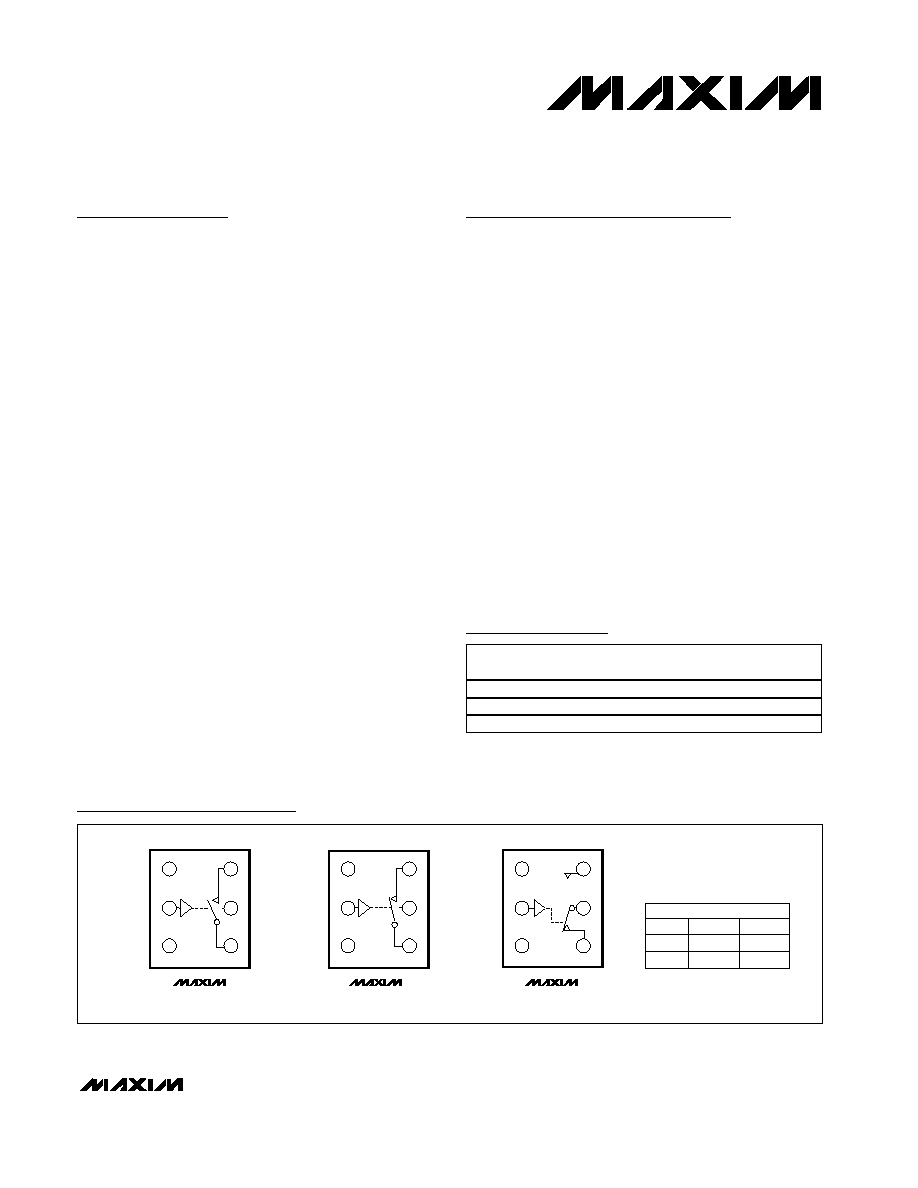
1
IN
COM
GND
NO
V+
TOP VIEW
IN
NC
GND
NO
COM
V+
MAX4688
SPDT
IN
COM
GND
NC
V+
MAX4687
SPST NC
MAX4686
SPST NO
MAX4686/MAX4687/MAX4688
IN
0
1
NO
OFF
ON
NC
ON
OFF
B3
I.C.
B1
A3
A2
A1
B2
B3
B1
A3
A2
A1
B2
I.C.
B3
B1
A3
A2
A1
B2
SWITCHES SHOWN FOR LOGIC "0"
Pin Configurations/Functional Diagrams/Truth Table
19-2042; Rev 1; 2/03
Ordering Information
PART
TEMP
RANGE
BUMP-
PACKAGE
TOP
MARK
MAX4686EBT-T
-40∞C to +85∞C
6 UCSP-6
AAI
MAX4687EBT-T
-40∞C to +85∞C
6 UCSP-6
AAJ
MAX4688EBT-T
-40∞C to +85∞C
6 UCSP-6
AAK
Rail-to-Rail is a registered trademark of Nippon Motorola, Ltd.
UCSP is a trademark of Maxim Integrated Products, Inc.
For pricing, delivery, and ordering information, please contact Maxim/Dallas Direct! at
1-888-629-4642, or visit Maxim's website at www.maxim-ic.com.
MAX4686/MAX4687/MAX4688
2.5
, Low-Voltage, SPST/SPDT
Analog Switches in UCSP Package
2
_______________________________________________________________________________________
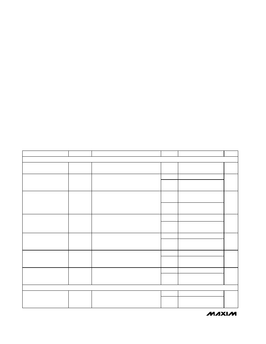
ABSOLUTE MAXIMUM RATINGS
ELECTRICAL CHARACTERISTICS
(V+ = +2.7V to +3.3V, V
IH
= +1.4V, V
IL
= 0.5V, T
A
= T
MIN
to T
MAX
, unless otherwise noted. Typical values are at 3V and T
A
= +25
∞C.)
(Notes 3, 4)
Stresses beyond those listed under "Absolute Maximum Ratings" may cause permanent damage to the device. These are stress ratings only, and functional
operation of the device at these or any other conditions beyond those indicated in the operational sections of the specifications is not implied. Exposure to
absolute maximum rating conditions for extended periods may affect device reliability.
All Voltages Referenced to GND
V+, IN .......................................................................-0.3V to +6V
COM, NO, NC (Note1)..................................-0.3V to (V+ + 0.3V)
Continuous Current NO, NC, COM ................................±100mA
Peak Current NO, NC, COM
(pulsed at 1ms, 10% duty cycle) ...............................±200mA
Continuous Power Dissipation (T
A
= +70∞C)
3 x 2 UCSP (derate 10.1mW/∞C at +70∞C) ..................808mW
Operating Temperature Range ...........................-40∞C to +85∞C
Storage Temperature Range ............................-65∞C to +150∞C
Bump Reflow Temperature .............................................+235∞C
PARAMETER
SYMBOL
CONDITIONS
T
A
MIN
TYP
MAX
U N IT S
ANALOG SWITCH
Analog Signal Range
V
COM
, V
NO
,
V
NC
T
MIN
to
T
MAX
0
V+
V
+25∞C
1.5
2.5
On-Resistance
R
ON
V+ = 2.7V, V
NC
= 0 to V+,
I
COM
= 10mA
T
MIN
to
T
MAX
3.5
+25∞C
0.3
0.4
On-Resistance Match
Between Channels
(MAX4688 only)
(Note 5)
R
ON
V+ = 2.7V, V
NO
or V
NC
= 1.5V,
I
COM
= 10mA
T
MIN
to
T
MAX
0.5
+25∞C
0.5
1
On-Resistance Flatness
(Note 6)
R
FLAT(ON)
V+ = 2.7V, V
NO
or V
NC
= 0 to V+,
I
COM
= 10mA
T
MIN
to
T
MAX
1
+25∞C
-0.5
±0.01
+0.5
NO, NC Off-Leakage
Current (Note 7)
I
NO(OFF)
,
I
NC(OFF)
V+ = 3.3V; V
COM
= 0.3V or 3V;
V
NO
or V
NC
= 3V, 0.3V
T
MIN
to
T
MAX
-1
1
nA
+25∞C
-0.5
±0.01
0.5
COM Off-Leakage
Current (Note 7)
I
COM_(OFF)
V+ = 3.3V; V
COM
= 0.3V or 3V;
V
NO
or V
NC
= 3V, 0.3V
T
MIN
to
T
MAX
-1
1
nA
+25∞C
-0.5
±0.01
0.5
COM On-Leakage
Current (Note 7)
I
COM_(ON)
V+ = 3.3V; V
COM
= 3V or 0.3V;
V
NO
or V
NC
= 3V, 0.3V, or floating
T
MIN
to
T
MAX
-1
1
nA
DYNAMIC CHARACTERISTICS
+25∞C
20
30
Turn-On Time (Note 7)
t
ON
V
NO
or V
NC
= 1.5V, Figure 2
T
MIN
to
T
MAX
35
ns
Note 1: Signals on NO, NC, and COM exceeding V+ are clamped by an internal diode. Limit forward-diode current to maximum cur-
rent rating.
Note 2: This device is constructed using a unique set of packaging techniques that impose a limit on the thermal profile the device
can be exposed to during board level solder attach and rework. This limit permits only the use of the solder profiles recom-
mended in the industry standard specification, JEDEC 020A, paragraph 7.6, Table 3 for IR/VPR and convection reflow.
Preheating is requied. Hand or wave soldering is not allowed.

MAX4686/MAX4687/MAX4688
2.5
, Low-Voltage, SPST/SPDT
Analog Switches in UCSP Package
_______________________________________________________________________________________
3
Note 3: The algebraic convention, where the most negative value is a minimum and the most positive value a maximum, is used in
this data sheet.
Note 4: UCSP parts are 100% tested at +25
∞C only and guaranteed by correlation at the full hot-rated temperature.
Note 5:
R
ON
= R
ON(MAX
) - R
ON(MIN)
, between switches.
Note 6: Flatness is defined as the difference between the maximum and minimum value of on-resistance as measured over the
specified analog signal ranges.
Note 7: Guaranteed by design.
Note 8: Off Isolation = 20log
10
(V
COM
/ V
NO
), V
COM
= output, V
NO
= input to off switch.
Note 9: Between switches.
PARAMETER
SYMBOL
CONDITIONS
T
A
MIN
TYP
MAX
UNITS
+25∞C
10
12
Turn-Off Time (Note 7)
t
OFF
V
NO
or V
NC
= 1.5V, Figure 2
T
MIN
to
T
MAX
15
ns
+25∞C
8
Break-Before-Make
(MAX4688 only) (Note 7)
t
BBM
V
NO
, V
NC
= 1.5V, Figure 3
T
MIN
to
T
MAX
2
ns
Charge Injection
Q
V
GEN
= 0, R
GEN
= 0,
C
L
= 1.0nF, Figure 4
+25∞C
40
pC
On-Channel -3dB
Bandwidth
BW
Signal = 0dBm, 50
in and out,
Figure 5
+25∞C
200
MHz
Off-Isolation (Note 8)
V
ISO
C
L
= 5pF, R
L
= 50
, f = 100kHz,
Figure 5
+25∞C
-90
dB
Crosstalk (MAX4688
only) (Note 9)
V
CR
C
L
= 5pF, R
L
= 50
, f = 100kHz,
Figure 5
+25∞C
-95
dB
Total Harmonic
Distortion
THD
R
L
= 600
, 2Vp-p, f = 20Hz to 20kHz
+25∞C
0.06
%
NO, NC Off-
Capacitance
C
NO(OFF)
,
C
NC(OFF)
f = 1MHz, Figure 6
+25∞C
12
pF
COM Off-Capacitance
C
COM(OFF)
f = 1MHz, Figure 6
+25∞C
12
pF
Switch On-Capacitance
C
(ON)
f = 1MHz, Figure 6
+25∞C
35
pF
DIGITAL I/O
Input Logic High
V
IH
T
MIN
to
T
MAX
1.4
V
Input Logic Low
V
IL
T
MIN
to
T
MAX
0.5
V
Logic Input
Leakage Current
I
IH
,
I
IL
V
IN
= 0 or V+
T
MIN
to
T
MAX
-1
1
µA
POWER SUPPLY
Power-Supply Range
V+
T
MIN
to
T
MAX
1.8
5.5
V
Supply Current
I+
V+ = 3.3V, V
IN
= 0 or V+
T
MIN
to
T
MAX
-1
1
µA
ELECTRICAL CHARACTERISTICS (continued)
(V+ = +2.7V to +3.3V, V
IH
= +1.4V, V
IL
= 0.5V, T
A
= T
MIN
to T
MAX
, unless otherwise noted. Typical values are at 3V and T
A
= +25
∞C.)
(Notes 3, 4)

MAX4686/MAX4687/MAX4688
2.5
, Low-Voltage, SPST/SPDT
Analog Switches in UCSP Package
4
_______________________________________________________________________________________
0
6
3
12
9
15
18
-40
10
-15
35
60
85
TURN-ON/OFF TIME vs. TEMPERATURE
MAX4686/7/8 toc07
TEMPERATURE (
∞C)
t
ON/OFF
(ns)
t
ON
t
OFF
V+ = +3V
1000
100
10
1
0.1
-40
10
-15
35
60
85
ON/OFF-LEAKAGE CURRENT
vs. TEMPERATURE
MAX4686/7/8 toc08
TEMPERATURE (
∞C)
ON/OFF-LEAKAGE CURRENT (pA)
V+ = +3V
I
NOOFF,
I
NCOFF
I
COMON
80
60
40
20
0
0
2
1
3
4
5
CHARGE INJECTION vs. V
COM
MAX4686/7/8 toc09
V
COM
(V)
Q (pC)
V+ = +5V
V+ = +3V
0
4
2
8
6
10
12
0
2
3
1
4
5
6
SUPPLY CURRENT vs. SUPPLY VOLTAGE
MAX4686/7/8 toc01
SUPPLY VOLTAGE (V)
SUPPLY CURRENT (pA)
1.0
2.0
1.5
3.0
2.5
3.5
4.0
0
2
1
3
4
5
ON-RESISTANCE vs. V
COM
MAX4686/7/8 toc02
V
COM
(V)
R
ON
(
)
V+ = +2.7V
V+ = +3.3V
V+ = +5V
V+ = +1.8V
0.5
1.0
2.0
1.5
2.5
3.0
0
1.0
0.5
1.5
2.0
2.5
3.0
ON-RESISTANCE vs. V
COM
(V+ = +3V)
MAX4686/7/8 toc03
V
COM
(V)
R
ON
(
)
T
A
= +85
∞C
T
A
= -40
∞C
T
A
= +25
∞C
0.5
1.1
0.9
0.7
1.3
1.5
1.7
1.9
2.1
2.3
2.5
0
2
1
3
4
5
ON-RESISTANCE vs. V
COM
(V+ = +5V)
MAX4686/7/8 toc04
V
COM
(V)
R
ON
(
)
T
A
= +85
∞C
T
A
= +25
∞C
T
A
= -40
∞C
0
0.5
1.0
1.5
2.0
1.5
2.5
3.5
4.5
2.0
3.0
4.0
5.0
5.5
LOGIC THRESHOLD VOLTAGE
vs. SUPPLY VOLTAGE
MAX4686/7/8 toc05
V+ (V)
LOGIC THRESHOLD VOLTAGE (V)
V
IN
FALLING
V
IN
RISING
0
10
5
20
15
30
25
35
1
3
2
4
5
6
TURN-ON/OFF TIME vs. SUPPLY VOLTAGE
MAX4686/7/8 toc06
V+ (V)
t
ON/OFF
(ns)
t
OFF
t
ON
Typical Operating Characteristics
(T
A
= +25∞C, unless otherwise noted.)

Applications Information
Logic Inputs
Where the MAX4686/MAX4687/MAX4688 have a +3.3V
supply, IN may be driven low to GND and driven high
to 5.5V. Driving IN rail-to-rail minimizes power con-
sumption. Logic inputs accept up to +5.5V regardless
of supply voltage.
Analog Signal Levels
Analog signals that range over the entire supply volt-
age (V+ to GND) are passed with very little change in
R
ON
(see Typical Operating Characteristics). The
switches are bidirectional, so the NO, NC, and COM
pins are both inputs or outputs.
Power-Supply Sequencing
and Overvoltage Protection
CAUTION: Do not exceed the absolute maximum
ratings because stresses beyond the listed ratings
may cause permanent damage to devices.
MAX4686/MAX4687/MAX4688
2.5
, Low-Voltage, SPST/SPDT
Analog Switches in UCSP Package
_______________________________________________________________________________________
5
Pin Description
BUMP
MAX4686
MAX4687
MAX4688
NAME
FUNCTION
B1
B1
B1
V+
Positive Supply Voltage Input
B2
B2
B2
IN
Digital Control Input
B3
B3
B3
GND
Ground
--
A1
A3
NC
Analog Switch, Normally Closed Terminal
A3
A3
A2
COM
Analog Switch, Common Terminal
A1
--
A1
NO
Analog Switch, Normally Open Terminal
A2
A2
--
I.C.
Internally Connected
0
-120
0.01
1
10
0.1
100
FREQUENCY RESPONSE
MAX4686/7/8 toc10
FREQUENCY (MHz)
LOSS (dB)
-100
-80
-60
-40
-20
ON-RESPONSE
OFF-ISOLATION
CROSSTALK
10
1k
100k
TOTAL HARMONIC DISTORTION PLUS
NOISE vs. FREQUENCY
MAX4686/7/8 toc11
FREQUENCY (Hz)
THD + N (%)
1
0.01
0.1
100
10k
Typical Operating Characteristics (continued)
(T
A
= +25∞C, unless otherwise noted.)
Figure 1. Overvoltage Protection Using External Blocking
Diodes
POSITIVE SUPPLY
COM
NO
D1
GND
Vg
V+
MAX4686
MAX4687
MAX4688