 | –≠–Ľ–Ķ–ļ—ā—Ä–ĺ–Ĺ–Ĺ—č–Ļ –ļ–ĺ–ľ–Ņ–ĺ–Ĺ–Ķ–Ĺ—ā: MAX472 | –°–ļ–į—á–į—ā—Ć:  PDF PDF  ZIP ZIP |

_______________General Description
The MAX471/MAX472 are complete, bidirectional, high-
side current-sense amplifiers for portable PCs, tele-
phones, and other systems where battery/DC
power-line monitoring is critical. High-side power-line
monitoring is especially useful in battery-powered sys-
tems, since it does not interfere with the ground paths
of the battery chargers or monitors often found in
"smart" batteries.
The MAX471 has an internal 35m
current-sense resis-
tor and measures battery currents up to Ī3A. For appli-
cations requiring higher current or increased flexibility,
the MAX472 functions with external sense and gain-set-
ting resistors. Both devices have a current output that
can be converted to a ground-referred voltage with a
single resistor, allowing a wide range of battery volt-
ages and currents.
An open-collector SIGN output indicates current-flow
direction, so the user can monitor whether a battery is
being charged or discharged. Both devices operate
from 3V to 36V, draw less than 100ĶA over tempera-
ture, and include a 18ĶA max shutdown mode.
________________________Applications
Portable PCs:
Notebooks/Subnotebooks/Palmtops
Smart Battery Packs
Cellular Phones
Portable Phones
Portable Test/Measurement Systems
Battery-Operated Systems
Energy Management Systems
____________________________Features
o
Complete High-Side Current Sensing
o
Precision Internal Sense Resistor (MAX471)
o
2% Accuracy Over Temperature
o
Monitors Both Charge and Discharge
o
3A Sense Capability with Internal Sense Resistor
(MAX471)
o
Higher Current-Sense Capability with External
Sense Resistor (MAX472)
o
100ĶA Max Supply Current
o
18ĶA Max Shutdown Mode
o
3V to 36V Supply Operation
o
8-Pin DIP/SO Packages
______________Ordering Information
MAX471/MAX472
Precision, High-Side
Current-Sense Amplifiers
________________________________________________________________
Maxim Integrated Products
1
1
2
3
4
8
7
6
5
OUT
RS-
RS-
SIGN
GND
RS+
RS+
SHDN
MAX471
DIP/SO
TOP VIEW
_________________Pin Configurations
MAX471
RS+
RS+
RS-
RS-
SIGN
OUT
GND
SHDN
3V
TO
36V
100k
I
LOAD
2000
2k
I
LOAD
TO
LOAD or CHARGER
LOGIC
SUPPLY
DISCHARGE/CHARGE
V
OUT
(1V/A)
__________Typical Operating Circuit
19-0335; Rev 2; 12/96
PART
MAX471
CPA
MAX471CSA
MAX471EPA
-40įC to +85įC
0įC to +70įC
0įC to +70įC
TEMP. RANGE
PIN-PACKAGE
8 Plastic DIP
8 SO
8 Plastic DIP
MAX471ESA
-40įC to +85įC
8 SO
MAX472
CPA
0įC to +70įC
8 Plastic DIP
MAX472CSA
0įC to +70įC
8 SO
MAX472EPA
-40įC to +85įC
8 Plastic DIP
MAX472ESA
-40įC to +85įC
8 SO
MAX472 Pin Configuration continued on last page.
For free samples & the latest literature: http://www.maxim-ic.com, or phone 1-800-998-8800
MAX471/MAX472
Precision, High-Side
Current-Sense Amplifiers
2
_______________________________________________________________________________________
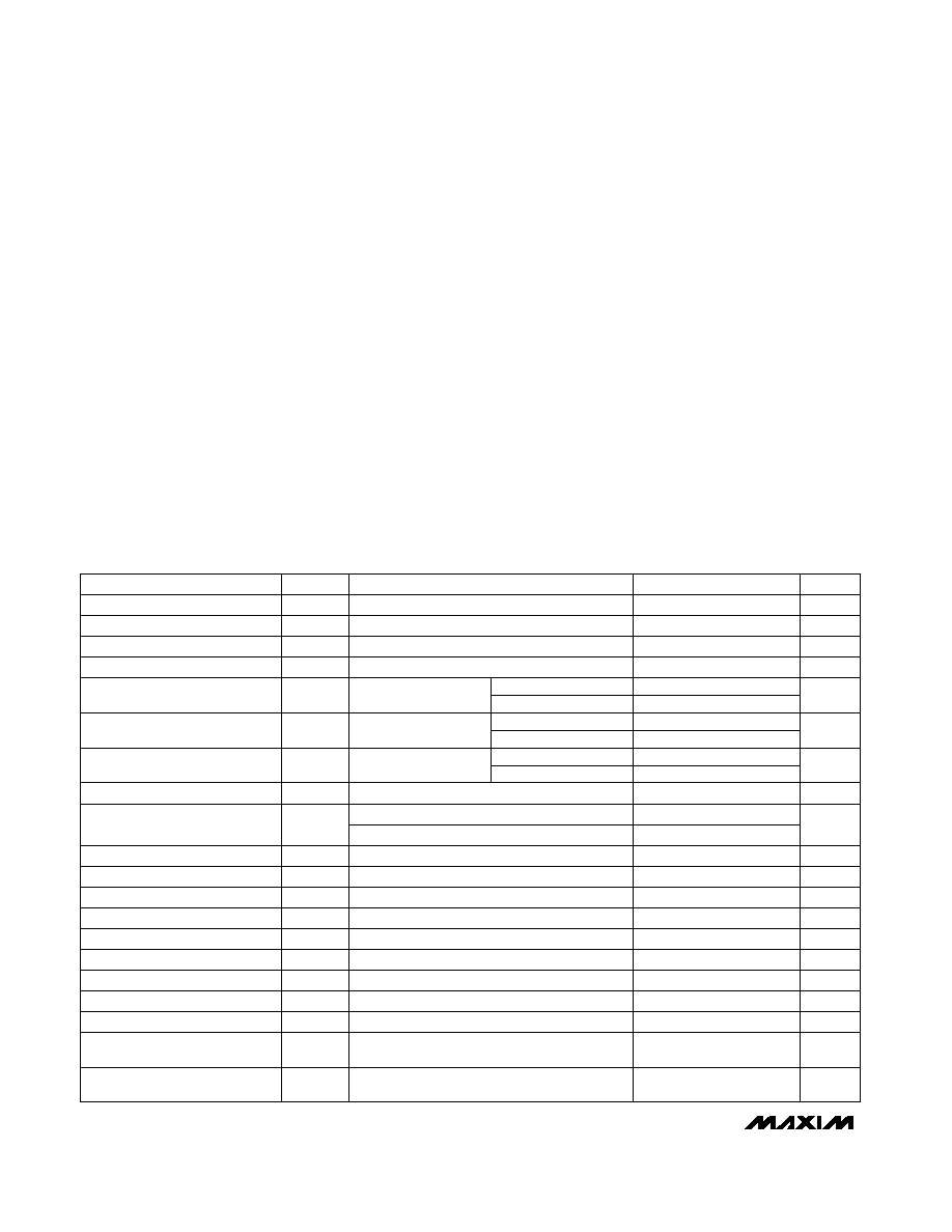
ABSOLUTE MAXIMUM RATINGS
ELECTRICAL CHARACTERISTICS--MAX471
(RS+ = +3V to +36V, T
A
= T
MIN
to T
MAX
, unless otherwise noted. Typical values are at T
A
= +25įC.)
Stresses beyond those listed under "Absolute Maximum Ratings" may cause permanent damage to the device. These are stress ratings only, and functional
operation of the device at these or any other conditions beyond those indicated in the operational sections of the specifications is not implied. Exposure to
absolute maximum rating conditions for extended periods may affect device reliability.
Supply Voltage, RS+, RS-, V
CC
to GND....................-0.3V, +40V
RMS Current, RS+ to RS- (MAX471 only)..........................Ī3.3A
Peak Current, (RS+ to RS-) ......................................see Figure 5
Differential Input Voltage, RG1 to RG2 (MAX472 only) .....Ī0.3V
Voltage at Any Pin Except SIGN
MAX471 only ...........................................-0.3V to (RS+ - 0.3V)
MAX472 only ..........................................-0.3V to (V
CC
+ 0.3V)
Voltage at SIGN......................................................-0.3V to +40V
Current into SHDN, GND, OUT, RG1, RG2, V
CC
................Ī50mA
Current into SIGN.................................................+10mA, -50mA
Continuous Power Dissipation (T
A
= +70įC)
MAX471 (Note 1):
Plastic DIP (derate 17.5mW/įC above +70įC) ..................1.4W
SO (derate 9.9mW/įC above +70įC) .............................791mW
MAX472 :
Plastic DIP (derate 9.09mW/įC above +70įC) ..............727mW
SO (derate 5.88mW/įC above +70įC) ...........................471mW
Operating Temperature Ranges
MAX47_C_A ........................................................0įC to +70įC
MAX47_E_A .....................................................-40įC to +85įC
Junction Temperature Range ............................-60įC to +150įC
Storage Temperature Range .............................-60įC to +160įC
Lead Temperature (soldering, 10sec) .............................+300įC
V
SHDN
= 2.4V
I
LOAD
= 0A, excludes I
SIGN
V
SHDN
= 0V
V
SHDN
= 2.4V; V
CC
= 3V to 20V
V
SIGN
= 0.3V
V
SIGN =
36V
I
LOAD
= 30mA,
RS+ = 10V
MAX471E
MAX471C
I
LOAD
= 0A,
RS+ = 10V
I
LOAD
= 1A,
RS+ = 10V
3V
RS+
36V, I
LOAD
= 1A
CONDITIONS
V
0
V
RS+
- 1.5
V
OUT
OUT Output Voltage Range
ĶA
1.0
I
IH
SHDN Input High Current
V
2.4
V
IH
SHDN Input High Voltage
ĶA
1.0
I
IL
SHDN Input Low Current
V
0.3
V
IL
SHDN Input Low Voltage
ĶA
1.5
18.0
I
RS+(SHDN)
Shutdown Supply Current
mA
0.1
I
OL
SIGN Sink Current
ĶA
1.0
SIGN Output Leakage Current
mA
Ī4.0
Ī6.0
SIGN Threshold (I
LOAD
required
to switch SIGN)
%/V
0.1
PSRR
Power-Supply Rejection Ratio
A
RMS
Ī3
I
LOAD
Sense Current
V
50
113
I
RS+
3
36
V
RS+
Supply Voltage
Supply Current
ĶA
Ī3.0
Low-Level OUT Error
Ī2.5
ĶA
3.0
No-Load OUT Error
m
35
70
R
SENSE
Sense Resistor
0.490
0.500
0.510
mA/A
0.4875
0.500
0.5125
I
OUT
/
I
LOAD
Current-Sense Ratio
2.5
UNITS
MIN
TYP
MAX
SYMBOL
PARAMETER
OUT Output Resistance
R
OUT
I
LOAD
= 3.0A, V
OUT
= 0V to (V
RS+
- 1.5V)
1
3
M
OUT Rise, Fall Time
t
R
, t
F
I
LOAD
= 50mA to 3.0A, R
OUT
= 2k
,
C
OUT
= 50pF, 10% to 90%
4
Ķs
OUT Settling Time to 1%
of Final Value
t
s
I
LOAD
= 100mA to 3.0A, R
OUT
= 2k
,
C
OUT
= 50pF
15
Ķs
MAX471C
MAX471C
MAX471C
MAX471E
MAX471E
MAX471E
Ī7.0
ĶA
Note 1:
Due to special packaging considerations, MAX471 (DIP, SO) has a higher power dissipation rating than the MAX472. RS+
and RS- must be soldered to large copper traces to achieve this dissipation rating.

MAX471/MAX472
Precision, High-Side
Current-Sense Amplifiers
_______________________________________________________________________________________
3
ELECTRICAL CHARACTERISTICS--MAX472
(V
CC
= +3V to +36V, RG1 = RG2 = 200
, T
A
= T
MIN
to T
MAX
, unless otherwise noted. Typical values are at T
A
= +25įC.)
Note 2:
V
OS
is defined as the input voltage (V
SENSE
) required to give minimum I
OUT
.
Note 3:
V
SENSE
is the voltage across the sense resistor.
V
SHDN
= 2.4V
MAX472C
V
SHDN
= 0V
I
LOAD
= 0A, excludes I
SIGN
; V
CC
= 3V to 20V
V
SHDN
= 2.4V; V
CC
= 3V to 20V
V
SIGN
= 0.3V
V
SIGN
= 36V
V
CC
= 10V,
V
SENSE
= 3mV
V
CC
= 10V
MAX472E
I
RG1
- I
GR2
3V
V
CC
36V, V
SENSE
= 100mV
CONDITIONS
V
0
V
CC
- 1.5
V
OUT
OUT Output Voltage Range
ĶA
1.0
I
IH
SHDN Input High Current
V
2.4
V
IH
SHDN Input High Voltage
ĶA
1.0
I
IL
SHDN Input Low Current
V
0.3
V
IL
SHDN Input Low Voltage
ĶA
1.5
18.0
I
CC(SHDN)
Shutdown Supply Current
mA
0.1
SIGN Output Sink Current
ĶA
1.0
SIGN Output Leakage Current
ĶV
60
140
SIGN Threshold (V
SENSE
required to switch SIGN)
60
120
%/V
0.1
PSRR
Power-Supply Rejection Ratio
120
ĶA
20
48
I
CC
V
3
36
V
CC
Supply Voltage
Supply Current
ĶA
Ī3.0
Low-Level OUT Error
Ī2.5
ĶA
2.5
ĶV
140
V
OS
Input Offset Voltage
(Note 2)
ĶA
20
35
I
RG1
, I
RG2
Input Bias Current
ĶA
Ī0.4
Ī3.0
I
OS
Input Bias-Current Matching
UNITS
MIN
TYP
MAX
SYMBOL
PARAMETER
OUT Output Resistance
R
OUT
I
OUT
= 1.5mA
1
3
M
OUT Rise, Fall Time
t
R
, t
F
V
SENSE
= 5mV to 150mV, R
OUT
= 2k
,
C
OUT
= 50pF, 10% to 90%
4
Ķs
OUT Settling Time to 1%
of Final Value
t
s
V
SENSE
= 5mV to 150mV, R
OUT
= 2k
,
C
OUT
= 50pF
15
Ķs
Maximum Output Current
I
OUT
1.5
mA
MAX472C
MAX472E
MAX472C
MAX472E
V
CC
= 10V,
V
SENSE
= 0V
3
No-Load OUT Error
MAX472C
MAX472E
V
SENSE
= 100mV,
V
CC
= 10V (Note 3)
I
RG
/I
OUT
OUT Current Accuracy
MAX472C
%
Ī2
MAX472E
Ī2.5
MAX471/MAX472
Precision, High-Side
Current-Sense Amplifiers
4
_______________________________________________________________________________________
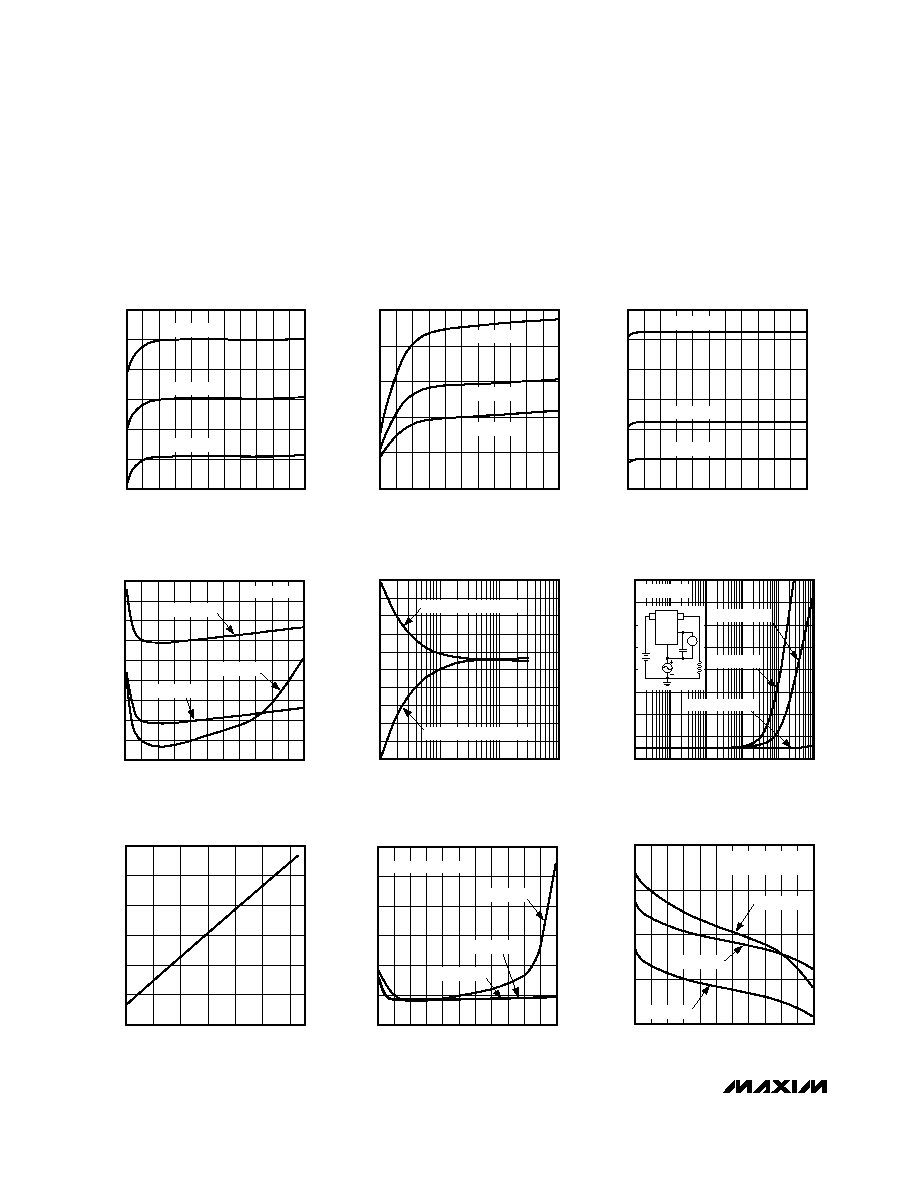
__________________________________________Typical Operating Characteristics
(Typical Operating Circuit (MAX471) or circuit of Figure 4, RG1 = RG2 = 200
, R
OUT
= 2k
(MAX472), T
A
= +25įC, unless
otherwise noted.)
65
35
SUPPLY CURRENT vs.
SUPPLY VOLTAGE
40
MAX1471-01
V
RS+
(V)
SUPPLY CURRENT (
Ķ
A)
21 24
15 18
9 12
3
6
27 30 33 36
45
50
55
60
T
A
= +85įC
T
A
= +25įC
T
A
= -40įC
2.5
0
0.5
2.0
MAX1471-02
I
SHDN
(
Ķ
A)
1.5
1.0
SHUTDOWN CURRENT vs.
SUPPLY VOLTAGE
V
RS+
(V)
21 24
15 18
9 12
3
6
27 30 33 36
T
A
= +85įC
T
A
= -40įC
T
A
= +25įC
4
-2
SIGN THRESHOLD vs.
SUPPLY VOLTAGE
-1
MAX1471-03
SIGN THRESHOLD (mA)
21 24
15 18
9 12
3
6
27 30 33 36
0
1
2
3
T
A
= +85įC
T
A
= +25įC
T
A
= -40įC
V
RS+
(V)
0.6
MAX1471-04
OFFSET CURRENT (
Ķ
A)
MAX471
NO-LOAD OFFSET CURRENT vs.
SUPPLY VOLTAGE
V
RS+
(V)
21 24
15 18
9 12
3
6
27 30 33 36
0.8
1.0
1.2
1.4
1.6
1.8
2.0
2.2
2.4
VS+ = VS-
T
A
= -40įC
T
A
= +85įC
T
A
= +25įC
28
-40
80
TEMPERATURE (įC)
RESISTANCE (m
)
20
30
-20
0
60
40
MAX1471-07
MAX471
RS+ TO RS- RESISTANCE vs.
TEMPERATURE
32
34
36
38
40
-12
0.01
0.10
MAX471
ERROR vs. LOAD CURRENT
MAX471-05
I
LOAD
(A)
ERROR (%)
1
10
-15
-6
-9
-3
0
3
6
9
12
15
I
LOAD
FROM RS+ TO RS-
I
LOAD
FROM RS- TO RS+
40
0.01
10
1000
MAX471
POWER-SUPPLY REJECTION RATIO
vs. FREQUENCY
MAX471-06
POWER-SUPPLY FREQUENCY (kHz)
PSRR (%)
1
100
35
30
25
20
15
10
5
0
0.10
V = 0mV TO 50mV
V = 0V TO 1V
V = 0V TO 0.5V
I
LOAD
= 1A
5V
RS+
OUT
GND
RS≠
A
1
Ķ
F
5
V
3.0
0
MAX472
NO-LOAD OUTPUT ERROR vs.
SUPPLY VOLTAGE
0.5
MAX1471-08
V
CC
(V)
I
OUT
(
Ķ
A)
21 24
15 18
9 12
3
6
27 30 33 36
1.0
1.5
2.0
2.5
T
A
= +85įC
T
A
= -40įC
T
A
= +25įC
RG1 = RG2 = 0
0.70
MAX1471-09
ERROR (%)
MAX472
ERROR vs. SUPPLY VOLTAGE
V
CC
(V)
21 24
15 18
9 12
3
6
27 30 33 36
V
RG1
-V
RG2
= 60mV,
RG1 = RG2 = 200
0.80
0.90
1.00
1.10
T
A
= -40įC
T
A
= +25įC
T
A
= +85įC
MAX471/MAX472
Precision, High-Side
Current-Sense Amplifiers
_______________________________________________________________________________________
5
25
-25
0.1
10
1000
MAX472
ERROR vs. SENSE VOLTAGE
MAX471-10
V
SENSE
(mV)
ERROR (%)
15
5
0
-5
-15
1
100
V
RG1
-V
RG2
V
RG2
-V
RG1
1mA
10mA
100mA
1A
0.1
0
0.2
0.3
0.4
0.5
MAX471
NOISE vs. LOAD CURRENT
ISENSE
I OUT
NOISE (ĶA
RMS
)
MAX471-15
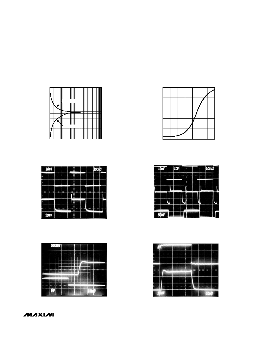
____________________________Typical Operating Characteristics (continued)
(Typical Operating Circuit (MAX471) or circuit of Figure 4, RG1 = RG2 = 200
, R
OUT
= 2k
(MAX472), T
A
= +25įC, unless
otherwise noted.)
100
Ķ
s/div
V
CC
= 10V, R
OUT
= 2k
1%, SIGN PULL-UP = 50k
1%
LOAD
CURRENT
50mA/div
V
OUT
50mV/div
MAX471
0mA to 100mA TRANSIENT RESPONSE
0A
10
Ķ
s/div
I
LOAD
= 1A, R
OUT
= 2k
1%
V
OUT
500mV/div
MAX471
START-UP DELAY
V
SHDN
5V/div
10
Ķ
s/div
R
OUT
= 2k
1%
I
LOAD
1A/div
MAX471
0A TO 3A TRANSIENT RESPONSE
V
OUT
10mV/div
100
Ķ
s/div
V
CC
= 10V, R
OUT
= 2k
1%, SIGN PULL-UP = 50k
1%
LOAD
CURRENT
100mA/div
50mA/div
50mA/div
V
OUT
50mV/div
MAX471
-100mA to +100mA TRANSIENT RESPONSE
SIGN
50mV/div
0A