 | ÐлекÑÑоннÑй компоненÑ: MAX4734 | СкаÑаÑÑ:  PDF PDF  ZIP ZIP |
Äîêóìåíòàöèÿ è îïèñàíèÿ www.docs.chipfind.ru
General Description
The MAX4734 is a low on-resistance, low-voltage, 4-
channel CMOS analog multiplexer that operates from a
single 1.6V to 3.6V supply. This device has fast switch-
ing speeds (t
ON
= 25ns, t
OFF
= 20ns max), handles
Rail-to-Rail
®
analog signals, and consumes less than
4µW of quiescent power. The MAX4734 has break-
before-make switching.
When powered from a 3V supply, the MAX4734 fea-
tures low 0.8
(max) on-resistance (R
ON
), with 0.2
(max) R
ON
matching and 0.1
R
ON
flatness. The digital
logic input is 1.8V CMOS compatible when using a sin-
gle 3V supply.
The MAX4734 is available in space-saving 12-pin QFN
(3mm x 3mm) and 10-pin µMAX packages.
Applications
Power Routing
Battery-Powered Systems
Audio and Video Signal Routing
Low-Voltage Data-Acquisition Systems
Communications Circuits
PCMCIA Cards
Cellular Phones
Modems
Hard Drives
Features
o Low R
ON
0.8
(max) (3V Supply)
2
(max) (1.8V Supply)
o 0.1 (max) R
ON
Flatness (3V Supply)
o 1.6V to 3.6V Single-Supply Operation
o Available in QFN (3mm x 3mm) Package
o High-Current Handling Capacity (150mA
Continuous)
o 1.8V CMOS-Logic Compatible (3V Supply)
o Fast Switching: t
ON
= 25ns, t
OFF
= 20ns
MAX4734
0.8
, Low-Voltage, 4-Channel
Analog Multiplexer
________________________________________________________________ Maxim Integrated Products
1
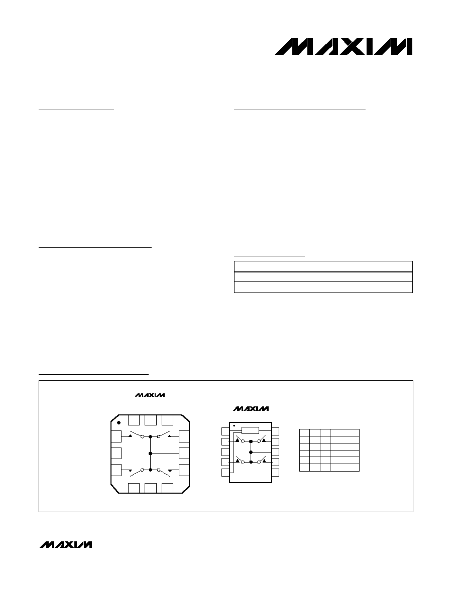
TOP VIEW
12
A0
11
N.C.
10
A1
9
NO2
8
COM
7
NO4
4
EN
5
N.C.
6
V+
1
NO1
2
GND
3
NO3
MAX4734
1
2
3
4
5
10
9
8
7
6
A1
NO2
COM
NO4
NO3
GND
NO1
A0
MAX4734
µMAX
V+
EN
LOGIC
A1 A0 EN ON SWITCH
X
X
0
NONE
0
0
1
1
0
1
1
2
1
0
1
3
1
1
1
4
X = DON'T CARE
QFN
Pin Configurations/Functional Diagrams/Truth Table
Ordering Information
19-2381; Rev 0; 4/02
For pricing, delivery, and ordering information, please contact Maxim/Dallas Direct! at
1-888-629-4642, or visit Maxim's website at www.maxim-ic.com.
PART
TEMP RANGE
PIN-PACKAGE
MAX4734EUB
-40°C to +85°C
10 µMAX
MAX4734EGC
-40°C to +85°C
12 QFN (3mm x 3mm)
Rail-to-Rail is a registered trademark of Nippon Motorola, Ltd.
MAX4734
0.8
, Low-Voltage, 4-Channel
Analog Multiplexer
2
_______________________________________________________________________________________
ABSOLUTE MAXIMUM RATINGS
ELECTRICAL CHARACTERISTICS--Single 3V Supply
(V+ = 2.7V to 3.6V, V
IH
= 1.4V, V
IL
= 0.5V, T
A
= T
MIN
to T
MAX
, unless otherwise specified. Typical values are at V+ = 3.0V,
T
A
= +25°C.) (Notes 2, 3)
Stresses beyond those listed under "Absolute Maximum Ratings" may cause permanent damage to the device. These are stress ratings only, and functional
operation of the device at these or any other conditions beyond those indicated in the operational sections of the specifications is not implied. Exposure to
absolute maximum rating conditions for extended periods may affect device reliability.
Note 1: Signals on COM or NO_ exceeding V+ or GND are clamped by internal diodes. Limit forward current to maximum current rating.
Voltages Referenced to GND
V+, A_, EN_ ..............................................................-0.3V to +4V
COM, NO_ (Note 1) ......................................-0.3V to (V+ + 0.3V)
Continuous Current COM, NO_ ......................................±150mA
Continuous Current (all other pins)...................................±20mA
Peak Current COM, NO_
(pulsed at 1ms 10% duty cycle)..................................±300mA
Continuous Power Dissipation (T
A
= +70°C)
10-Pin µMAX (derate 5.6mW/°C above +70°C) ............444mW
12-Pin QFN (derate 14.7mW/°C above +70°C) ..........1176mW
Operating Temperature Range ...........................-40°C to +85°C
Maximum Junction Temperature .....................................+150°C
Storage Temperature Range .............................-65°C to +150°C
Lead Temperature (soldering, 10s) .................................+300°C
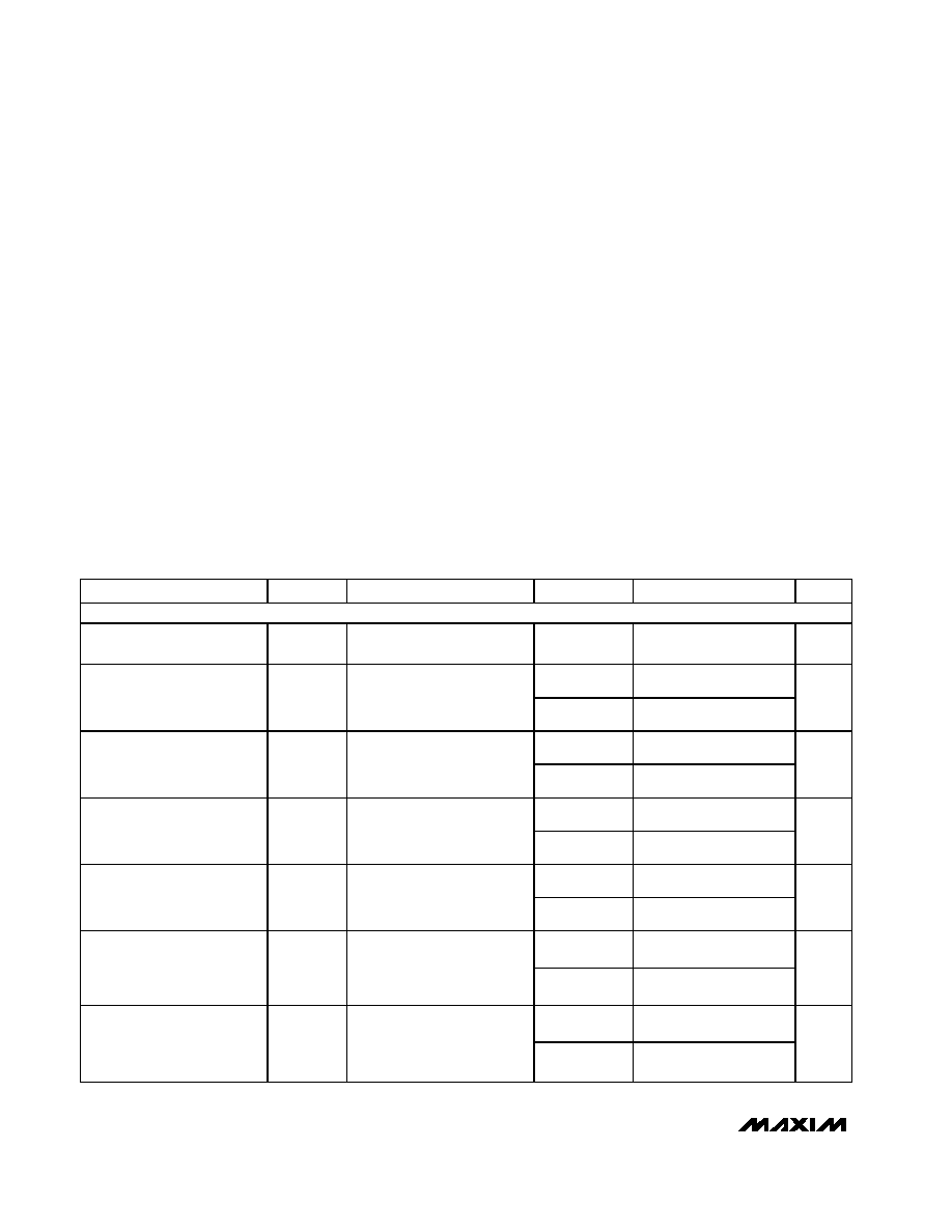
PARAMETER
SYMBOL
CONDITIONS
T
A
MIN
TYP
MAX
UNITS
ANALOG SWITCH
Analog Signal Range
V
COM
,
V
NO
_
0
V+
V
+25°C
0.6
0.8
On-Resistance (Note 4)
R
ON
V+ = 2.7V,
I
COM
= 100mA,
V
NO
_ = 1.5V
T
MIN
to T
MAX
1
+25°C
0.1
0.2
On-Resistance Match
Between Channels
(Notes 4, 5)
R
ON
V+ = 2.7V,
I
COM
= 100mA,
V
NO
_ = 1.5V
T
MIN
to T
MAX
0.3
+25°C
0.05
0.1
On-Resistance Flatness
(Note 6)
R
FLAT(ON)
V+ = 2.7V,
I
COM
_ = 100mA,
V
NO
_ = 1V, 1.5V, 2V
T
MIN
to T
MAX
0.2
+25°C
-1
±0.002
+1
NO_ Off-Leakage Current
(Note 7)
I
NO_(OFF)
V+ = 3.6V,
V
COM
= 0.3V, 3.3V,
V
NO
_ = 3.3V, 0.3V
T
MIN
to T
MAX
-5
+5
nA
+25°C
-1
±0.002
+1
COM Off-Leakage Current
(Note 7)
I
COM(OFF)
V+ = 3.6V,
V
COM
= 0.3V, 3.3V,
V
NO
_ = 3.3V, 0.3V
T
MIN
to T
MAX
-5
+5
nA
+25°C
-2
±0.002
+2
COM On-Leakage Current
(Note 7)
I
COM(ON)
V+ = 3.6V,
V
COM
= 3.3V, 0.3V,
V
NO
_ = 3.3V, 0.3V, or
floating
T
MIN
to T
MAX
-10
+10
nA
MAX4734
0.8
, Low-Voltage, 4-Channel
Analog Multiplexer
_______________________________________________________________________________________
3
ELECTRICAL CHARACTERISTICS--Single 3V Supply (continued)
(V+ = 2.7V to 3.6V, V
IH
= 1.4V, V
IL
= 0.5V, T
A
= T
MIN
to T
MAX
, unless otherwise specified. Typical values are at V+ = 3.0V,
T
A
= +25°C.) (Notes 2, 3)
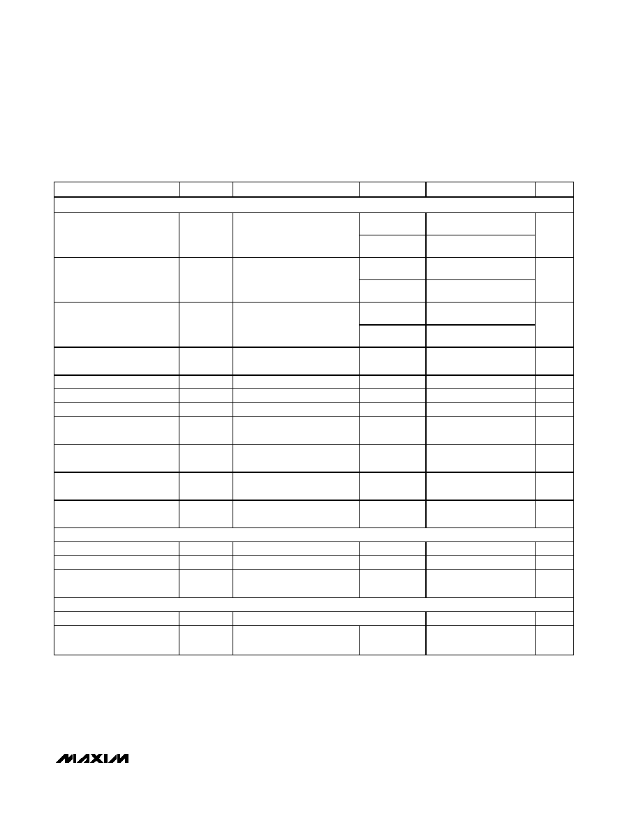
PARAMETER
SYMBOL
CONDITIONS
T
A
MIN
TYP
MAX
UNITS
SWITCH DYNAMIC CHARACTERISTICS
+25°C
20
25
Turn-On Time
t
ON
V
NO
_ = 1.5V,
R
L
= 50
, C
L
= 35pF,
Figure 1
T
MIN
to T
MAX
30
ns
+25°C
15
20
Turn-Off Time
t
OFF
V
NO
_ = 1.5V,
R
L
= 50
, C
L
= 35pF,
Figure 1
T
MIN
to T
MAX
25
ns
+25°C
5
Break-Before-Make (Note 8)
t
BBM
V
NO
_ = 1.5V,
R
L
= 50
, C
L
= 35pF,
Figure 2
T
MIN
to T
MAX
1
ns
Charge Injection
Q
V
GEN
= 0, R
GEN
= 0,
C
L
= 1.0nF, Figure 3
+25°C
60
pC
NO_ Off-Capacitance
C
OFF
f = 1MHz, Figure 4
+25°C
33
pF
COM Off-Capacitance
C
COM(OFF)
f = 1MHz, Figure 4
+25°C
117
pF
COM On-Capacitance
C
COM(ON)
f = 1MHz, Figure 4
+25°C
171
pF
-3dB On-Channel Bandwidth
BW
Signal = 0, R
IN
= R
OUT
=
50
, C
L
= 5pF, Figure 5
90
MHz
Off-Isolation (Note 9)
V
ISO
f = 1M H z, V
C OM
= 1V
P - P
, R
L
=
50
, C
L
= 5p F, Fi g ur e 5
+25°C
-56
dB
Crosstalk (Note 10)
V
CT
f = 1M H z, V
C OM
= 1V
P - P
, R
L
=
50
, C
L
= 5p F, Fi g ur e 5
+25°C
-56
dB
Total Harmonic Distortion
THD
f = 20Hz to 20kHz, V
COM
=
2V
P-P
, R
L
= 32
+25°C
0.018
%
LOGIC INPUT (A_, EN)
Input Logic High
V
IH
1.4
V
Input Logic Low
V
IL
0.5
V
Input Leakage Current
I
IN
V
EN
= 0 or 3.6V, V
A
_ = 0
or 3.6V
-1
0.005
+1
µA
POWER SUPPLY
Power-Supply Range
V+
1.6
3.6
V
Positive Supply Current
I+
V+ = 3.6V, V
EN, A
_ = 0 or
V+, all channels on or off
0.004
1
µA
MAX4734
0.8
, Low-Voltage, 4-Channel
Analog Multiplexer
4
_______________________________________________________________________________________
ELECTRICAL CHARACTERISTICS--Single 1.8V Supply
(V+ = 1.8V, V
IH
= 1.0V, V
IL
= 0.4V, T
A
= T
MIN
to T
MAX
, unless otherwise specified. Typical values are at T
A
= +25°C.) (Notes 2, 3)
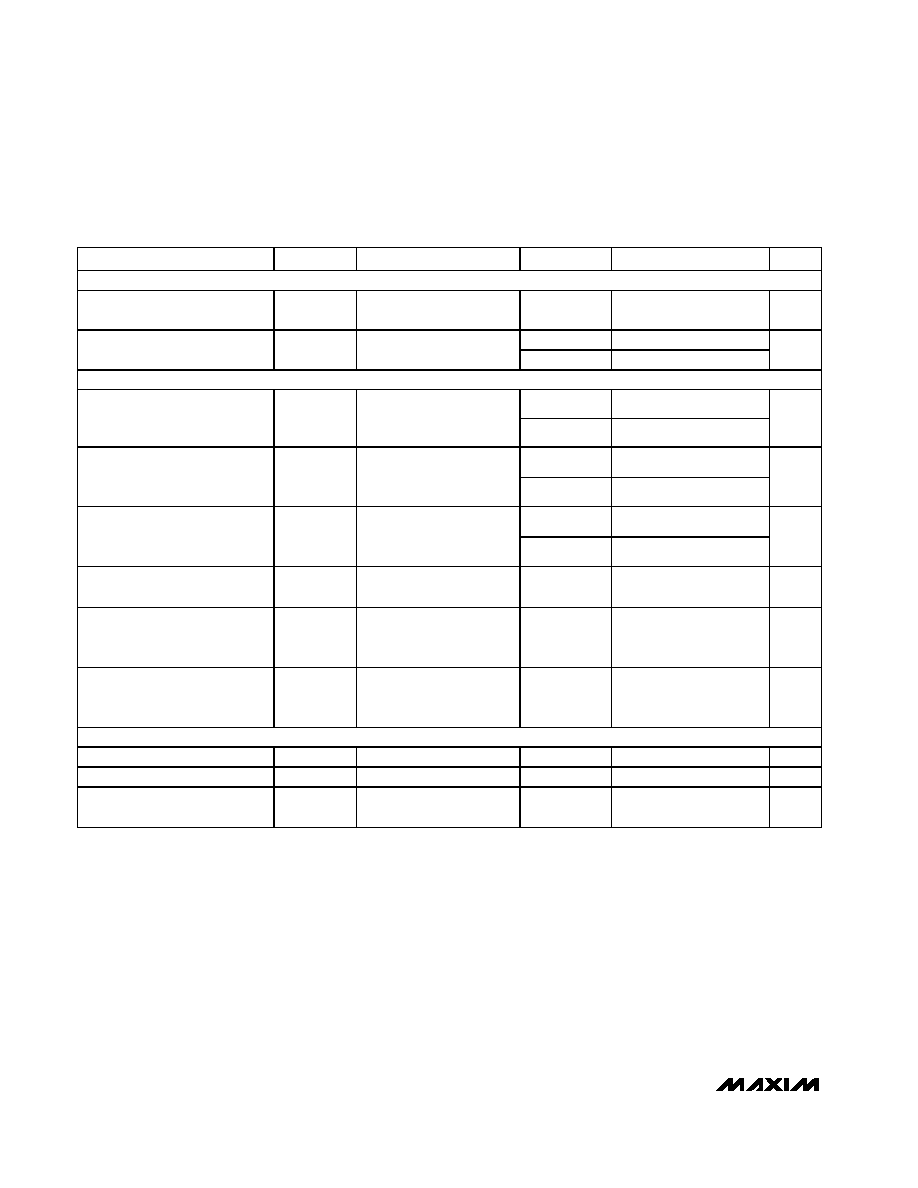
PARAMETER
SYMBOL
CONDITIONS
T
A
MIN
TYP
MAX
UNITS
ANALOG SWITCH
Analog Signal Range
V
COM
,
V
NO
_
0
V+
V
+25°C
1.5
2
On-Resistance
R
ON
I
COM
_ = 10mA,
V
NO
_ = 1V
T
MIN
to T
MAX
3
SWITCH DYNAMIC CHARACTERISTICS
+25°C
25
30
Turn-On Time
t
ON
V
NO
_ = 1V,
RL = 50
, C
L
= 35pF,
Figure 1
T
MIN
to T
MAX
35
ns
+25°C
18
25
Turn-Off Time
t
OFF
V
NO
_ = 1V,
R
L
= 50
, C
L
= 35pF,
Figure 1
T
MIN
to T
MAX
28
ns
+25°C
7
Break-Before-Make (Note 8)
t
BBM
V
NO
_ = 1V,
R
L
= 50
, C
L
= 35pF,
Figure 2
T
MIN
to T
MAX
1
ns
Charge Injection
Q
V
GEN
= 0, R
GEN
= 0,
C
L
= 1nF, Figure 3
+25°C
35
pC
Off-Isolation (Note 9)
V
ISO
f = 1M H z, V
N O
_
= 1V
P - P
, R
L
= 50
,
C
L
= 5p F, Fi g ur e 5
+25°C
-56
dB
Crosstalk (Note 10)
V
CT
f = 1M H z, V
C OM
= 1V
P - P
,
R
L
= 50
,
C
L
= 5p F, Fi g ur e 5
+25°C
-56
dB
LOGIC INPUT (A_, EN)
Input Logic High
V
IH
1
V
Input Logic Low
V
IL
0.4
V
Input Leakage Current
I
IN
V
EN
= 0 or 3.6V,
V
A_
= 0 or 3.6V
1
µA
Note 2: The algebraic convention, where the most negative value is a minimum and the most positive value is a maximum, is
used in this data sheet.
Note 3: -40°C specifications are guaranteed by design.
Note 4: R
ON
and
R
ON
matching specifications for QFN packaged parts are guaranteed by design.
Note 5:
R
ON
= R
ON(MAX)
- R
ON(MIN)
.
Note 6: Flatness is defined as the difference between the maximum and the minimum value of on-resistance as measured over
the specified analog signal ranges.
Note 7: Leakage parameters are 100% tested at hot temperature and guaranteed by correlation at room temperature.
Note 8: Guaranteed by design.
Note 9: Off-Isolation = 20log
10
(V
COM
/V
NO
_), V
COM
= output, V
NO
_ = input to off switch.
Note 10: Between two switches.
MAX4734
0.8
, Low-Voltage, 4-Channel
Analog Multiplexer
_______________________________________________________________________________________
5
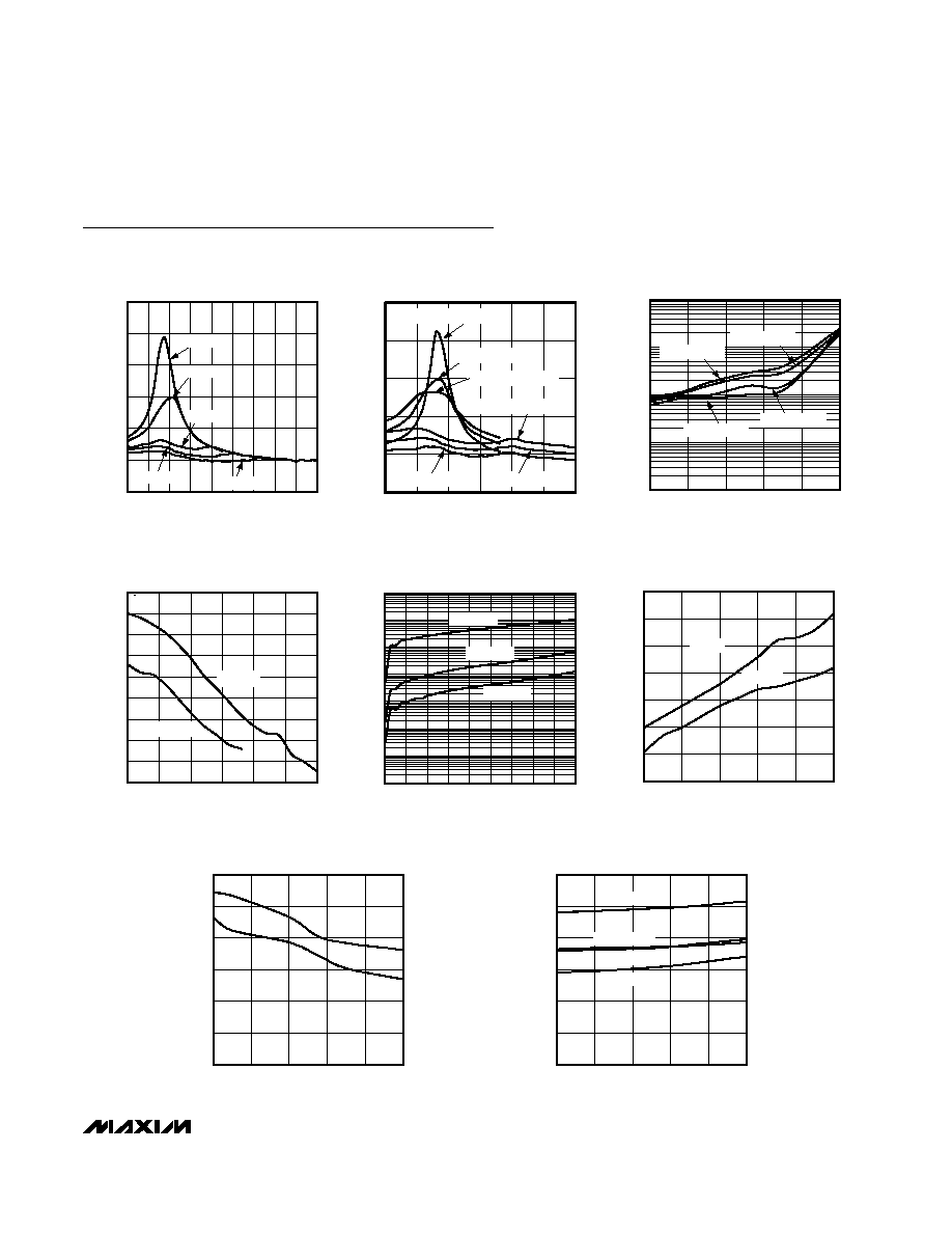
Typical Operating Characteristics
(T
A
= +25°C, unless otherwise noted.)
0
1.0
0.5
1.5
2.5
3.0
2.0
0
0.8 1.2
0.4
1.6 2.0 2.4 2.8 3.2 3.6
ON-RESISTANCE vs. V
COM
MAX4734 toc01
V
COM
(V)
R
ON
(
)
V+ = 1.6V
V+ = 1.8V
V+ = 2.5V
V+ = 3.0V
V+ = 3.6V
0
0.5
1.5
1.0
2.0
2.5
0
0.5
1.0
1.5
2.0
2.5
3.0
ON-RESISTANCE vs. V
COM
AND TEMPERATURE
MAX4734 toc02
V
COM
(V)
R
ON
(
)
V+ = 1.8V, T
A
= -40
°C
V+ = 1.8V, T
A
= +25
°C
V+ = 1.8V, T
A
= +85
°C
V+ = 3.0V, T
A
= +85
°C
V+ = 3.0V, T
A
= +25
°C
V+ = 3.0V, T
A
= -40
°C
ON/OFF-LEAKAGE CURRENT
vs. TEMPERATURE
MAX4734 toc03
TEMPERATURE (
°C)
LEAKAGE CURRENT (pA)
60
35
10
-15
10
100
1000
10,000
1
-40
85
OFF, V+ = 3.0V
ON, V+ = 3.0V
ON, V+ = 1.8V
OFF, V+ = 1.8V
-20
0
-10
30
20
10
60
50
40
70
0
1.0
0.5
2.0
2.5
3.0
CHARGE INJECTION vs. V
COM
MAX4734 toc04
V
COM
(V)
Q (pC)
V+ = 3.0V
V+ = 1.8V
1.5
1000
0.0001
0
0.4
2.0
2.8
SUPPLY CURRENT vs. SUPPLY
VOLTAGE AND TEMPERATURE
0.001
1
100
MAX4734 toc05
SUPPLY VOLTAGE (V)
SUPPLY CURRENT (nA)
1.6
3.6
10
0.1
0.01
0.8 1.2
3.2
2.4
T
A
= -40
°C
T
A
= +25
°C
T
A
= +85
°C
0.5
0.7
0.6
1.0
0.9
0.8
1.1
1.2
2.4
2.0
2.8
3.2
3.6
LOGIC-LEVEL THRESHOLD
vs. SUPPLY VOLTAGE
MAX4734 toc06
SUPPLY VOLTAGE (V)
THRESHOLD (V)
1.6
RISING
FALLING
TURN-ON/OFF TIME
vs. SUPPLY VOLTAGE
MAX4734 toc07
SUPPLY VOLTAGE (V)
t
ON
/t
OFF
(ns)
3.2
2.8
2.4
2.0
5
10
15
20
25
30
0
1.6
3.6
t
OFF
t
ON
TURN-ON/OFF TIME
vs. TEMPERATURE
MAX4734 toc08
TEMPERATURE (
°C)
t
ON
/t
OFF
(ns)
60
35
10
-15
5
10
15
20
25
30
0
-40
85
t
ON
, V+ = 1.8V
t
OFF
, V+ = 1.8V
t
ON
, V+ = 3.0V
t
OFF
, V+ = 3.0V