 | –≠–Ľ–Ķ–ļ—ā—Ä–ĺ–Ĺ–Ĺ—č–Ļ –ļ–ĺ–ľ–Ņ–ĺ–Ĺ–Ķ–Ĺ—ā: MAX5104 | –°–ļ–į—á–į—ā—Ć:  PDF PDF  ZIP ZIP |
General Description
The MAX5104 low-power, serial, voltage-output, dual
12-bit digital-to-analog converter (DAC) consumes only
500ĶA from a single +5V supply. This device features
Rail-to-Rail
ģ
output swing and is available in a space-
saving 16-pin QSOP package. To maximize the dynamic
range, the DAC output amplifiers are configured with an
internal gain of +2V/V.
The 3-wire serial interface is SPITM/QSPITM/MICROWIRETM
compatible. Each DAC has a double-buffered input
organized as an input register followed by a DAC register,
which allows the input and DAC registers to be updated
independently or simultaneously with a 16-bit serial
word. Additional features include programmable power-
down (2ĶA), hardware power-down lockout (PDL), a
separate reference voltage input for each DAC that
accepts AC and DC signals, and an active-low clear
input (CL) that resets all registers and DACs to zero.
These devices provide a programmable logic pin for
added functionality, and a serial-data output pin for
daisy chaining.
________________________Applications
Industrial Process Control
Remote Industrial Controls
Digital Offset and Gain Adjustment
Microprocessor-Controlled Systems
Motion Control
Automatic Test Equipment (ATE)
____________________________Features
o
12-Bit Dual DAC with Internal Gain of +2V/V
o
Rail-to-Rail Output Swing
o
12Ķs Settling Time
o
+5V Single-Supply Operation
o
Low Quiescent Current
500ĶA (normal operation)
2ĶA (power-down mode)
o
SPI/QSPI/MICROWIRE Compatible
o
Space-Saving 16-Pin QSOP Package
o
Power-On Reset Clears Registers and DACs to Zero
o
Adjustable Output Offset
MAX5104
Low-Power, Dual, Voltage-Output, 12-Bit DAC
with Serial Interface
________________________________________________________________
Maxim Integrated Products
1
19-1587; Rev 0; 11/99
Ordering Information
Rail-to-Rail is a registered trademark of Nippon Motorola, Ltd.
SPI and QSPI are trademarks of Motorola, Inc.
MICROWIRE is a trademark of National Semiconductor Corp.
For free samples & the latest literature: http://www.maxim-ic.com, or phone 1-800-998-8800.
For small orders, phone 1-800-835-8769.
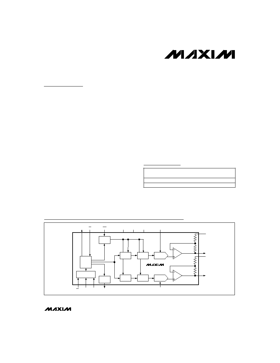
REFA
V
DD
AGND
DGND
PDL
CL
DOUT
16-BIT
SHIFT
REGISTER
SR
CONTROL
INPUT
REG A
INPUT
REG B
SCLK
UPOH
REFB
DIN
CS
DAC B
DAC A
DAC
REG A
LOGIC
OUTPUT
DECODE
CONTROL
DAC
REG B
MAX5104
OUTB
R
R
R
R
OSB
OUTA
OSA
Functional Diagram
Pin Configuration appears at end of data sheet.
PIN-
PACKAGE
TEMP. RANGE
PART
16 QSOP
16 QSOP
0įC to +70įC
-40įC to +85įC
MAX5104EEE
MAX5104CEE
INL
(LSB)
Ī4
Ī4
MAX5104
Low-Power, Dual, Voltage-Output, 12-Bit DAC
with Serial Interface
2
_______________________________________________________________________________________
ABSOLUTE MAXIMUM RATINGS
ELECTRICAL CHARACTERISTICS
(V
DD
= +5V Ī10%, V
REFA
= V
REFB
= +2.048V, R
L
= 10k
, C
L
= 100pF, T
A
= T
MIN
to T
MAX
, unless otherwise noted. Typical values
are at T
A
= +25įC (OS_ connected to AGND for a gain of +2V/V).)
Stresses beyond those listed under "Absolute Maximum Ratings" may cause permanent damage to the device. These are stress ratings only, and functional
operation of the device at these or any other conditions beyond those indicated in the operational sections of the specifications is not implied. Exposure to
absolute maximum rating conditions for extended periods may affect device reliability.
V
DD
to AGND............................................................-0.3V to +6V
V
DD
to DGND ...........................................................-0.3V to +6V
AGND to DGND ..................................................................Ī0.3V
OSA, OSB to AGND.......................(V
AGND
- 4V) to (V
DD
+ 0.3V)
REF_, OUT_ to AGND.................................-0.3V to (V
DD
+ 0.3V)
Digital Inputs (SCLK, DIN,
CS,
CL, PDL) to DGND ...........................................(-0.3V to +6V)
Digital Outputs (DOUT, UPO) to DGND .....-0.3V to (V
DD
+ 0.3V)
Maximum Current into Any Pin .........................................Ī20mA
Continuous Power Dissipation (T
A
= +70įC)
16-Pin QSOP (derate 8.30mW/įC above +70įC).......667mW
Operating Temperature Ranges
MAX5104CEE ...................................................0įC to +70įC
MAX5104EEE.................................................-40Cį to +85įC
Junction Temperature ......................................................+150įC
Storage Temperature Range .............................-65įC to +150įC
Lead Temperature (soldering, 10sec) .............................+300įC
REFERENCE INPUT
DIGITAL INPUTS
Input Hysteresis
V
HYS
200
mV
Input Capacitance
C
IN
8
pF
Input Leakage Current
I
IN
0.001
Ī1
ĶA
V
IN
= 0 to V
DD
Input Low Voltage
V
IL
0.8
V
CL, PDL, CS, DIN, SCLK
Signal-to-Noise plus
Distortion Ratio
SINAD
75
dB
Input code = 1FFE hex,
V
REF_
= 1Vp-p at 1.25V
DC
, f = 25kHz
PARAMETER
SYMBOL
MIN
TYP
MAX
UNITS
CONDITIONS
Gain Error
-0.2
Ī8
LSB
Offset Tempco
TCV
OS
4
ppm/įC
Offset Error
V
OS
Ī10
mV
Differential Nonlinearity
DNL
Ī1
LSB
Gain-Error Tempco
4
ppm/įC
20
600
ĶV/V
V
DD
Power-Supply
Rejection Ratio
PSRR
Integral Nonlinearity
Resolution
12
Bits
INL
Ī4
LSB
Reference Input Resistance
R
REF
14
20
k
Reference 3dB Bandwidth
300
kHz
Reference Feedthrough
-82
dB
Normalized to 2.048V
Code = 10
Guaranteed monotonic
Normalized to 2.048V
Minimum with code 1554 hex
4.5V
V
DD
5.5V
Input code = 1FFE hex,
V
REF_
= 0.67Vp-p at 2.5V
DC
Input code = 0000 hex,
V
REF_
= (V
DD
- 1.4Vp-p), f = 1kHz
(Note 1)
STATIC PERFORMANCE
Reference Input Range
0
V
DD
- 1.4
V
REF
MULTIPLYING-MODE PERFORMANCE
Input High Voltage
V
IH
3
V
CL, PDL, CS, DIN, SCLK
MAX5104
Low-Power, Dual, Voltage-Output, 12-Bit DAC
with Serial Interface
_______________________________________________________________________________________
3
ELECTRICAL CHARACTERISTICS (continued)
(V
DD
= +5V Ī10%, V
REFA
= V
REFB
= +2.048V, R
L
= 10k
, C
L
= 100pF, T
A
= T
MIN
to T
MAX
, unless otherwise noted. Typical values
are at T
A
= +25įC (OS_ connected to AGND for a gain of +2V/V).)
Note 1:
Accuracy is specified from code 6 to code 4095.
Note 2:
Accuracy is better than 1LSB for V
OUT_
greater than 6mV and less than V
DD
- 50mV. Guaranteed by PSRR test at the
end points.
Note 3:
Digital inputs are set to either V
DD
or DGND, code = 0000 hex, R
L
=
.
Note 4:
SCLK minimum clock period includes the rise and fall times.
CS = V
DD
, SCLK = 100kHz, V
SCLK
= 5Vp-p
I
SOURCE
= 2mA
(Note 4)
(Note 3)
(Note 3)
ns
Rail-to-rail (Note 2)
To 1/2LSB of full-scale, V
STEP
= 4V
40
I
SINK
= 2mA
t
CL
SCLK Pulse Width Low
CONDITIONS
ns
40
t
CH
SCLK Pulse Width High
nVs
5
Digital Crosstalk
nVs
5
Digital Feedthrough
Ķs
25
Time Required to Exit Shutdown
k
24
34
R
OS_
OSA or OSB Input Resistance
ns
100
t
CP
SCLK Clock Period
ĶA
0
Ī1
Reference Current in Shutdown
ĶA
2
10
I
DD(SHDN)
Power-Supply Current
in Shutdown
mA
0.5
0.65
I
DD
Power-Supply Current
V
4.5
5.5
V
DD
Positive Supply Voltage
ns
40
t
DS
SDI Setup Time
ns
V
V
DD
- 0.5
V
OH
Output High Voltage
0
t
CSH
SCLK Rise to
CS Rise
Hold Time
ns
40
t
CSS
CS Fall to SCLK Rise
Setup Time
C
LOAD
= 200pF
V
0 to V
DD
Output Voltage Swing
Ķs
15
Output Settling Time
C
LOAD
= 200pF
ns
80
V
0.13
0.40
V
OL
Output Low Voltage
V/Ķs
0.75
SR
Voltage Output Slew Rate
UNITS
MIN
TYP
MAX
SYMBOL
PARAMETER
t
DO2
SCLK Fall to DOUT
Valid Propagation Delay
ns
80
t
DO1
SCLK Rise to DOUT
Valid Propagation Delay
ns
0
t
DH
SDI Hold Time
ns
100
t
CSW
CS Pulse Width High
ns
40
t
CS1
CS Rise to SCLK Rise Hold
ns
10
t
CS0
SCLK Rise to
CS Fall Delay
DIGITAL OUTPUTS
(DOUT, UPO)
DYNAMIC PERFORMANCE
POWER SUPPLIES
TIMING CHARACTERISTICS

MAX5104
Low-Power, Dual, Voltage-Output, 12-Bit DAC
with Serial Interface
4
_______________________________________________________________________________________
__________________________________________Typical Operating Characteristics
(V
DD
= +5V, R
L
= 10k
, C
L
= 100pF, OS_ pins connected to AGND, T
A
= +25įC, unless otherwise noted.)
-20
-16
-18
-12
-14
-8
-10
-6
-2
-4
0
1
370
740
1110
1480
1850
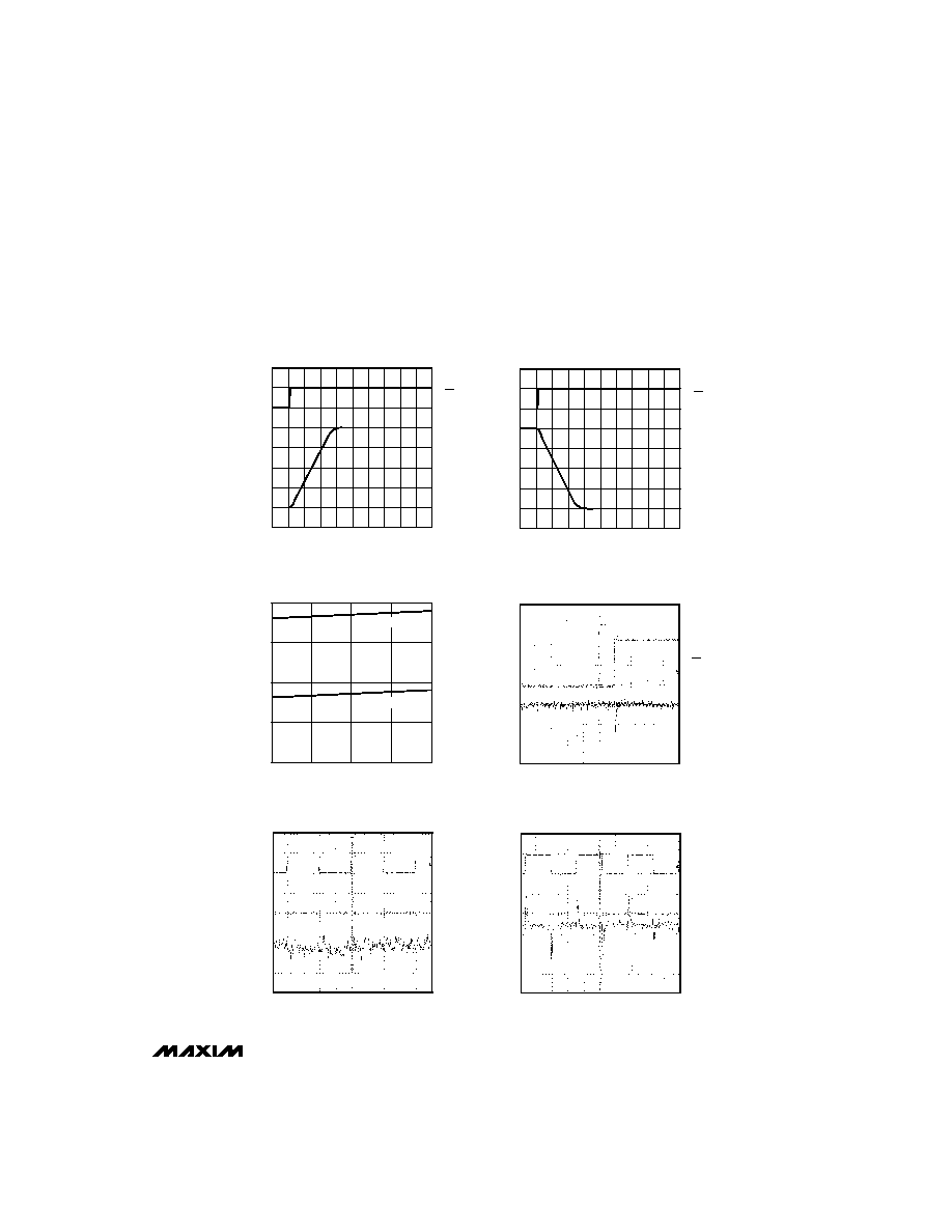
REFERENCE VOLTAGE INPUT
FREQUENCY RESPONSE
MAX5104 toc01
FREQUENCY (kHz)
RELATIVE OUTPUT (dB)
V
REF
= +0.67Vp-p AT 2.5V
DC
CODE = 1FFE (HEX)
400
450
550
500
650
600
700
-55
5
-15
-35
45
25
65
105
85
125
SUPPLY CURRENT vs. TEMPERATURE
MAX5104 toc02
TEMPERATURE (įC)
SUPPLY CURRENT (
Ķ
A)
V
REF
= +2.048V
R
L
=
CODE = 1FFE (HEX)
CODE = 0000 (HEX)
-30
-80
1
10
100
TOTAL HARMONIC DISTORTION
PLUS NOISE vs. FREQUENCY
-70
MAX5104 toc03
FREQUENCY (kHz)
THD + N (dB)
-60
-50
-40
V
REF
= +1Vp-p AT 2.5V
DC
CODE = 1FFE (HEX)
0
0.1
1
10
100
FULL-SCALE ERROR vs. RESISTIVE LOAD
-1.25
-1.00
-1.50
-0.75
-0.50
-0.25
0.25
0.50
MAX5104 toc04
R
L
(k
)
FULL-SCALE ERROR (LSB)
V
REF
= +2.048V
-100
-80
-90
-60
-70
-40
-50
0.5
1.6
2.7
3.8
4.9
6.0
-30
-10
-20
0
OUTPUT FFT PLOT
MAX5104 toc07
V
REF
= +2.45Vp-p AT 1.225V
DC
f = 1kHz
CODE = 1FFE (HEX)
NOTE: RELATIVE TO FULL SCALE
FREQUENCY (kHz)
RELATIVE OUTPUT (dB)
-150
-130
-140
-110
-120
-90
-100
-80
-60
-70
-50
0.5
1.5 2.0 2.5
1.0
3.0 3.5 4.0
5.0
4.5
5.5
REFERENCE FEEDTHROUGH AT 1kHz
MAX5104 toc05
FREQUENCY (kHz)
RELATIVE OUTPUT (dB)
V
REF
= +3.6Vp-p AT 1.88V
DC
CODE = 0000 (HEX)
0
1
2
3
4
5
6
-55
5
25
-15
-35
45
65
85 105 125
SHUTDOWN CURRENT
vs. TEMPERATURE
MAX5104 toc06
TEMPERATURE (įC)
SHUTDOWN CURRENT (
Ķ
A)
V
REF
= +1V
MAX5104
Low-Power, Dual, Voltage-Output, 12-Bit DAC
with Serial Interface
_______________________________________________________________________________________
5
_____________________________Typical Operating Characteristics (continued)
(V
DD
= +5V, R
L
= 10k
, C
L
= 100pF, OS_ pins connected to AGND, T
A
= +25įC, unless otherwise noted.)
0.40
0.45
0.50
0.55
0.60
4.50
4.75
5.00
5.25
5.50
SUPPLY CURRENT vs. SUPPLY VOLTAGE
MAX51504 toc10
SUPPLY VOLTAGE (V)
SUPPLY CURRENT (mA)
CODE = 1FFE (HEX)
CODE = OOOO (HEX)
OUTB
200
Ķ
V/div
AC-COUPLED
OUTA
5V/div
ANALOG CROSSTALK
MAX5104 toc12
V
REF
= +2.048V, GAIN = +2V/V, CODE = 1FFE HEX
250
Ķ
s/div
DIGITAL FEEDTHROUGH
MAX5104 toc13
OUTA
500
Ķ
V/div
AC-COUPLED
SCLK
5V/div
2.5
Ķ
s/div
5
Ķ
s/div
MAJOR-CARRY TRANSITION
MAX5104 toc11
TRANSITION FROM 1000 (HEX) TO 0FFE (HEX)
OUT_
50mV/div
AC-COUPLED
2V/div
CS
DYNAMIC RESPONSE RISE TIME
MAX5104 toc08
2
Ķ
s/div
OUT_
1V/div
5V/div
CS
V
REF
= +2.048V
2
Ķ
s/div
DYNAMIC RESPONSE FALL TIME
MAX5104 toc09
OUT_
1V/div
5V/div
CS
V
REF
= +2.048V