 | –≠–ª–µ–∫—Ç—Ä–æ–Ω–Ω—ã–π –∫–æ–º–ø–æ–Ω–µ–Ω—Ç: MAX5122 | –°–∫–∞—á–∞—Ç—å:  PDF PDF  ZIP ZIP |

For free samples & the latest literature: http://www.maxim-ic.com, or phone 1-800-998-8800.
For small orders, phone 1-800-835-8769.
General Description
The MAX5122/MAX5123 low-power, 12-bit, voltage-out-
put, digital-to-analog converters (DACs) feature an inter-
nal precision bandgap reference and output amplifier.
The MAX5122 operates on a single +5V supply with an
internal +2.5V reference, and offers a configurable output
amplifier. If necessary, the user can override the on-chip,
<10ppm/∞C voltage reference with an external reference.
The MAX5123 has the same features as the MAX5122 but
operates from a single +3V supply and has an internal
+1.25V precision reference. The user-accessible inverting
input and output of the amplifier allows specific gain con-
figurations, remote sensing, and high output drive capa-
bility for a wide range of force/sense applications. Both
devices draw only 500µA of supply current, which
reduces to 3µA in power-down mode. In addition, their
power-up reset feature allows for a user-selectable initial
output state of either 0V or midscale and reduces output
glitches during power-up.
The serial interface is compatible with SPITM, QSPITM, and
MICROWIRETM, which makes the MAX5122/MAX5123
suitable for cascading multiple devices. Each DAC has
a double-buffered input organized as an input register
followed by a DAC register. A 16-bit shift register loads
data into the input register. The DAC register may be
updated independently or simultaneously with the input
register.
Both devices are available in a 16-pin QSOP package
and are specified for the extended-industrial (-40∞C to
+85∞C) operating temperature range. For pin-compatible
14-bit upgrades, see the MAX5171/MAX5173 data sheet;
for the pin-compatible 13-bit version, see the MAX5132/
MAX5133 data sheet.
Applications
Industrial Process Control
Automatic Test Equipment
Digital Offset and Gain Adjustment
Motion Control
Microprocessor-Controlled Systems
Features
o
Single-Supply Operation
+5V (MAX5122)
+3V (MAX5123)
o
Built-In 10ppm/∞C max Precision Bandgap Reference
+2.5V (MAX5122)
+1.25V (MAX5123)
o
SPI/QSPI/MICROWIRE-Compatible, 3-Wire Serial
Interface
o
Pin-Programmable Shutdown Mode and Power-
Up Reset (0 or Midscale Output Voltage)
o
Buffered Output Capable of Driving 5k
100pF
or 4≠20mA Loads
o
Space-Saving 16-Pin QSOP Package
o
Pin-Compatible 13-Bit Upgrades Available
(MAX5132/MAX5133)
o
Pin-Compatible 14-Bit Upgrades Available
(MAX5171/MAX5173)
MAX5122/MAX5123
+5V/+3V, 12-Bit, Serial, Force/Sense DACs
with 10ppm/∞C Internal Reference
________________________________________________________________
Maxim Integrated Products
1
16
15
14
13
12
11
10
9
1
2
3
4
5
6
7
8
FB
V
DD
REFADJ
REF
AGND
PD
UPO
DOUT
DGND
TOP VIEW
MAX5122
MAX5123
QSOP
OUT
RSTVAL
CS
PDL
CLR
DIN
SCLK
19-1446; Rev 0; 3/99
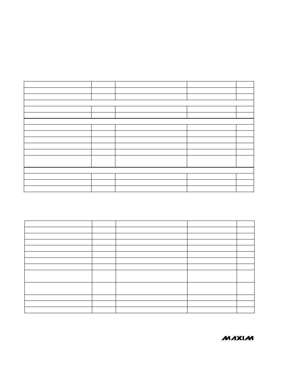
PART
MAX5122
AEEE
MAX5122BEEE
-40∞C to +85∞C
-40∞C to +85∞C
TEMP. RANGE
PIN-
PACKAGE
16 QSOP
16 QSOP
Pin Configuration
Ordering Information
INL
(LSB)
±0.5
±1
MAX5123
AEEE
MAX5123BEEE
±1
-40∞C to +85∞C
-40∞C to +85∞C
16 QSOP
16 QSOP
±2
SPI and QSPI are trademarks of Motorola, Inc.
MICROWIRE is a trademark of National Semiconductor Corp.

MAX5122/MAX5123
+5V/+3V, 12-Bit, Serial, Force/Sense DACs
with 10ppm/∞C Internal Reference
2
_______________________________________________________________________________________
ABSOLUTE MAXIMUM RATINGS
ELECTRICAL CHARACTERISTICS--MAX5122 (+5V)
(V
DD
= +5V ±10%, AGND = DGND, 33nF capacitor at REFADJ, internal reference, R
L
= 5k
, C
L
= 100pF, output amplifier configured
in unity-gain, T
A
= T
MIN
to T
MAX
, unless otherwise noted. Typical values are at T
A
= +25∞C.)
Stresses beyond those listed under "Absolute Maximum Ratings" may cause permanent damage to the device. These are stress ratings only, and functional
operation of the device at these or any other conditions beyond those indicated in the operational sections of the specifications is not implied. Exposure to
absolute maximum rating conditions for extended periods may affect device reliability.
V
DD
to AGND, DGND ...............................................-0.3V to +6V
AGND to DGND.....................................................-0.3V to +0.3V
Digital Inputs to DGND.............................................-0.3V to +6V
Digital Outputs (DOUT, UPO) to DGND .....-0.3V to (V
DD
+ 0.3V)
FB, OUT to AGND ......................................-0.3V to (V
DD
+ 0.3V)
REF, REFADJ to AGND ..............................-0.3V to (V
DD
+ 0.3V)
Maximum Current into Any Pin............................................50mA
Continuous Power Dissipation (T
A
= +70∞C)
QSOP (derate 8.00mW/∞C above +70∞C) .....................667mW
Operating Temperature Range ...........................-40∞C to +85∞C
Storage Temperature Range .............................-65∞C to +150∞C
Lead Temperature (soldering, 10sec) .............................+300∞C
V
IN
= 0 or V
DD
MAX5122A
REFADJ = V
DD
4.5V
V
DD
5.5V
MAX5123B
MAX5122B
MAX5122A
MAX5122A
T
A
= +25∞C
CONDITIONS
pF
8
C
IN
Input Capacitance
µA
-1
0.001
1
I
IN
Input Leakage Current
mV
200
V
HYS
Input Hysteresis
V
0.8
V
IL
Input Low Voltage
V
3
V
IH
Input High Voltage
µA
3.3
7
REFADJ Current
ppm/∞C
10
TCV
REF
3
Output Voltage Temperature
Coefficient
V
2.475
2.5
2.525
V
REF
Output Voltage
-0.5
0.5
Bits
12
N
Resolution
µV/V
20
250
PSRR
Power-Supply Rejection Ratio
ppm/∞C
10
30
TCV
FS
3
10
Full-Scale Temperature
Coefficient (Note 3)
LSB
-1
1
DNL
Differential Nonlinearity
mV
-10
10
V
OS
Offset Error (Note 2)
mV
-3
-0.2
3
GE
Gain Error
UNITS
MIN
TYP
MAX
SYMBOL
PARAMETER
I
SINK
= 2mA
I
SOURCE
= 2mA
V
0.13
0.4
V
OL
Output Low Voltage
V
V
DD
- 0.5
V
OH
Output High Voltage
MAX5123B
LSB
-1
1
INL
Integral Nonlinearity (Note 1)
0
I
OUT
100µA (sourcing)
µV/µA
0.1
1
V
OUT
/I
OUT
Reference External Load Regulation
mA
4
Reference Short-Circuit Current
STATIC PERFORMANCE
REFERENCE
DIGITAL INPUT
DIGITAL OUTPUTS

MAX5122/MAX5123
+5V/+3V, 12-Bit, Serial, Force/Sense DACs
with 10ppm/∞C Internal Reference
_______________________________________________________________________________________
3
ELECTRICAL CHARACTERISTICS--MAX5122 (+5V) (continued)
(V
DD
= +5V ±10%, AGND = DGND, 33nF capacitor at REFADJ, internal reference, R
L
= 5k
, C
L
= 100pF, output amplifier configured
in unity-gain, T
A
= T
MIN
to T
MAX
, unless otherwise noted. Typical values are at T
A
= +25∞C.)
To ±0.5LSB, V
STEP
= 2.5V
CS = V
DD
, f
SCLK
= 100kHz,
V
SCLK
= 5Vp-p
CONDITIONS
µA
3
20
I
SHDN
Power-Supply Current in Shutdown
µA
500
600
I
DD
Power-Supply Current (Note 5)
V
4.5
5.5
V
DD
Power-Supply Voltage (Note 5)
nV-sec
5
Digital Feedthrough
ms
2
Time Required to Exit Shutdown
µs
20
Output Settling Time
V
0 to V
DD
Output Voltage Swing (Note 4)
UNITS
MIN
TYP
MAX
SYMBOL
PARAMETER
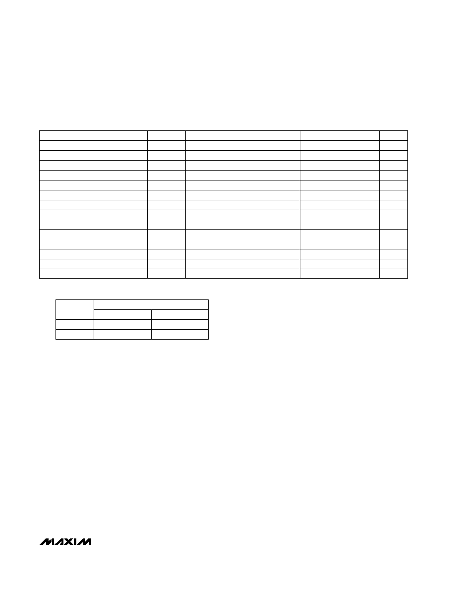
ELECTRICAL CHARACTERISTICS--MAX5123 (+3V)
(V
DD
= +3V ±10%, AGND = DGND, 33nF capacitor at REFADJ, internal reference, R
L
= 5k
, C
L
= 100pF, output amplifier connected
in unity-gain, T
A
= T
MIN
to T
MAX
, unless otherwise noted. Typical values are at T
A
= +25∞C.)
MAX5123A
REFADJ = V
DD
2.7V
V
DD
3.3V
MAX5123B
MAX5123B
MAX5123A
MAX5123A
T
A
= +25∞C
CONDITIONS
mV
200
V
HYS
Input Hysteresis
V
0.8
V
IL
Input Low Voltage
V
2.2
V
IH
Input High Voltage
µA
3.3
7
REFADJ Current
mA
4
Reference Short-Circuit Current
ppm/∞C
10
TCV
REF
MAX5123B
3
0
I
OUT
100µA (sourcing)
Output Voltage Temperature
Coefficient
V
1.237
1.25
1.263
V
REF
Output Voltage
-1
1
µV/µA
0.1
1
Bits
12
N
Resolution
µV/V
20
250
PSRR
Power-Supply Rejection Ratio
ppm/∞C
10
30
TCV
FS
LSB
3
10
V
OUT
/I
OUT
Full-Scale Temperature
Coefficient (Note 3)
LSB
-1
1
DNL
Differential Nonlinearity
mV
-10
10
V
OS
Offset Error (Note 2)
Reference External Load Regulation
mV
-5
-0.2
5
GE
Gain Error
UNITS
MIN
TYP
MAX
SYMBOL
PARAMETER
-2
2
INL
Integral Nonlinearity (Note 1)
V/µs
0.6
SR
Voltage Output Slew Rate
STATIC PERFORMANCE
REFERENCE
DIGITAL INPUT
µA
-0.1
0
0.1
Current into FB
DYNAMIC PERFORMANCE
POWER REQUIREMENTS
MAX5122/MAX5123
+5V/+3V, 12-Bit, Serial, Force/Sense DACs
with 10ppm/∞C Internal Reference
4
_______________________________________________________________________________________
ELECTRICAL CHARACTERISTICS--MAX5123 (+3V) (continued)
(V
DD
= +3V ±10%, AGND = DGND, 33nF capacitor at REFADJ, internal reference, R
L
= 5k
, C
L
= 100pF, output amplifier connected
in unity-gain, T
A
= T
MIN
to T
MAX
, unless otherwise noted. Typical values are at T
A
= +25∞C.)
To ±0.5LSB, V
STEP
= 1.25V
CS = V
DD
, f
SCLK
= 100kHz,
V
SCLK
= 3Vp-p
CONDITIONS
µA
3
20
I
SHDN
Power-Supply Current in Shutdown
µA
500
600
I
DD
Power-Supply Current (Note 5)
V
2.7
3.6
V
DD
Power-Supply Voltage (Note 5)
nV-sec
5
Digital Feedthrough
ms
2
Time Required to Exit Shutdown
µA
-0.1
0
0.1
Current into FB
µs
20
Output Settling Time
V
0 to V
DD
Output Voltage Swing (Note 4)
UNITS
MIN
TYP
MAX
SYMBOL
PARAMETER
I
SINK
= 2mA
V
0.13
0.4
V
OL
Output Low Voltage
I
SOURCE
= 2mA
V
V
DD
- 0.5
V
OH
Output High Voltage
V
IN
= 0 or V
DD
µA
-1
0.001
1
I
IN
Input Leakage Current
pF
8
C
IN
Input Capacitance
V/µs
0.6
SR
Voltage Output Slew Rate
TIMING CHARACTERISTICS--MAX5122 (+5V)
(V
DD
= +5V ±10%, AGND = DGND, 33nF capacitor at REFADJ, internal reference, R
L
= 5k
, C
L
= 100pF, output amplifier connected
in unity-gain, T
A
= T
MIN
to T
MAX
, unless otherwise noted. Typical values are at T
A
= +25∞C.)
ns
40
t
CSS
CS Fall to SCLK Rise Setup Time
ns
40
t
CL
SCLK Pulse Width Low
CONDITIONS
ns
100
t
CP
SCLK Clock Period
ns
40
t
CH
SCLK Pulse Width High
ns
0
t
CSH
SCLK Rise to CS Rise Hold Time
ns
10
t
CS0
SCLK Rise to CS Fall Delay Time
ns
40
t
DS
SDI Setup Time
ns
0
t
DH
SDI Hold Time
UNITS
MIN
TYP
MAX
SYMBOL
PARAMETER
ns
100
t
CSW
CS Pulse Width High
ns
40
t
CS1
CS Rise to SCLK Rise Hold Time
C
LOAD
= 200pF
ns
80
t
DO1
SCLK Rise to DOUT Valid
Propagation Delay Time
C
LOAD
= 200pF
ns
80
t
DO2
SCLK Fall to DOUT Valid
Propagation Delay Time
DIGITAL OUTPUTS
POWER REQUIREMENTS
DYNAMIC PERFORMANCE
MAX5122/MAX5123
+5V/+3V, 12-Bit, Serial, Force/Sense DACs
with 10ppm/∞C Internal Reference
_______________________________________________________________________________________
5
Note 1:
Accuracy is guaranteed by the following table:
Note 2:
Offset is measured at the code closest to 10mV.
Note 2:
The temperature coefficient is determined by the "box" method, in which the maximum
V
OUT
over the temperature range
is divided by
T and the typical reference voltage.
Note 4:
Accuracy is better than 1.0LSB for V
OUT
= 10mV to (V
DD
- 180mV). Guaranteed by PSR test on end points.
Note 5:
R
LOAD
=
and digital inputs are at either V
DD
or DGND.
TIMING CHARACTERISTICS--MAX5123 (+3V)
(V
DD
= +3V ±10%, AGND = DGND, 33nF capacitor at REFADJ, internal reference, R
L
= 5k
, C
L
= 100pF, output amplifier connected
in unity-gain, T
A
= T
MIN
to T
MAX
, unless otherwise noted. Typical values are at T
A
= +25∞C.)
ns
60
t
CSS
CS Fall to SCLK Rise Setup Time
ns
150
ns
C
LOAD
= 200pF
75
t
CSW
t
CL
SCLK Pulse Width Low
CONDITIONS
ns
150
t
CP
SCLK Clock Period
ns
75
t
CH
SCLK Pulse Width High
ns
0
t
CSH
SCLK Rise to CS Rise Hold Time
CS Pulse Width High
ns
75
t
CS1
CS Rise to SCLK Rise Hold Time
C
LOAD
= 200pF
ns
200
t
DO1
SCLK Rise to DOUT Valid
Propagation Delay Time
ns
200
t
DO2
SCLK Fall to DOUT Valid
Propagation Delay Time
ns
10
t
CS0
SCLK Rise to CS Fall Delay Time
ns
60
t
DS
SDI Setup Time
ns
0
t
DH
SDI Hold Time
UNITS
MIN
TYP
MAX
SYMBOL
PARAMETER
16
5
33
3
4095
4095
Accuracy Guaranteed
To Code:
From Code:
V
DD
(V)