 | ÐлекÑÑоннÑй компоненÑ: MAX5142 | СкаÑаÑÑ:  PDF PDF  ZIP ZIP |
Äîêóìåíòàöèÿ è îïèñàíèÿ www.docs.chipfind.ru
General Description
The MAX5141MAX5144 are serial-input, voltage-output,
14-bit digital-to-analog converters (DACs) in tiny µMAX
packages, 50% smaller than comparable DACs in an
8-pin SO. They operate from low +3V (MAX5143/
MAX5144) or +5V (MAX5141/MAX5142) single supplies.
They provide 14-bit performance (±1LSB INL and DNL)
over temperature without any adjustments. The DAC out-
put is unbuffered, resulting in a low supply current of
120µA and a low offset error of 2LSBs.
The DAC output range is 0V to V
REF.
For bipolar opera-
tion, matched scaling resistors are provided in the
MAX5142/MAX5144 for use with an external precision op
amp (such as the MAX400), generating a ±V
REF
output
swing.
A 16-bit serial word is used to load data into the DAC
latch. The 25MHz, 3-wire serial interface is compatible
with SPITM/QSPITM/MICROWIRETM, and can interface
directly with optocouplers for applications requiring isola-
tion. A power-on reset circuit clears the DAC output to
code 0 (MAX5141/MAX5143) or code 8192 (MAX5142/
MAX5144) when power is initially applied.
A logic low on CLR asynchronously clears the DAC out-
put to code 0 (MAX5141/MAX5143) or code 8192
(MAX5142/MAX5144), independent of the serial interface.
The MAX5141/MAX5143 are available in 8-pin µMAX
packages and the MAX5142/MAX5144 are available in
10-pin µMAX packages.
Applications
High-Resolution and Gain Adjustment
Industrial Process Control
Automated Test Equipment
Data-Acquisition Systems
Features
o Miniature (3mm x 5mm) 8-Pin µMAX Package
o Low 120µA Supply Current
o Fast 1µs Settling Time
o 25MHz SPI/QSPI/MICROWIRE-Compatible Serial
Interface
o V
REF
Range Extends to V
DD
o +5V (MAX5141/MAX5142) or +3V
(MAX5143/MAX5144) Single-Supply Operation
o Full 14-Bit Performance Without Adjustments
o Unbuffered Voltage Output Directly Drives 60k
Loads
o Power-On Reset Circuit Clears DAC Output to
Code 0 (MAX5141/MAX5143) or Code 8192
(MAX5142/MAX5144)
o Schmitt-Trigger Inputs for Direct Optocoupler
Interface
o Asynchronous CLR
MAX5141MAX5144
+3V/+5V, Serial-Input,
Voltage-Output, 14-Bit DACs
________________________________________________________________ Maxim Integrated Products
1
19-1849; Rev 1; 5/01
Ordering Information
SPI and QSPI are trademarks of Motorola, Inc.
MICROWIRE is a trademark of National Semiconductor Corp.
For pricing, delivery, and ordering information, please contact Maxim/Dallas Direct! at
1-888-629-4642, or visit Maxim's website at www.maxim-ic.com.
PART
T EM P. RA N G E
PIN - PAC K A GE
IN L ( L SB )
SU PPL Y
R A NG E ( V)
O U TPU T SWING
M A X5 1 4 1E U A
-40
°C to +85°C
8 µMAX
± 1
5
U nip ol ar
M A X5 1 4 2E U B
-40
°C to +85°C
10 µMAX
± 1
5
Bi pol ar
M A X5 1 4 3E U A
-40
°C to +85°C
8 µMAX
± 1
3
U nip ol ar
M A X5 1 4 4E U B
-40
°C to +85°C
10 µMAX
± 1
3
Bi pol ar
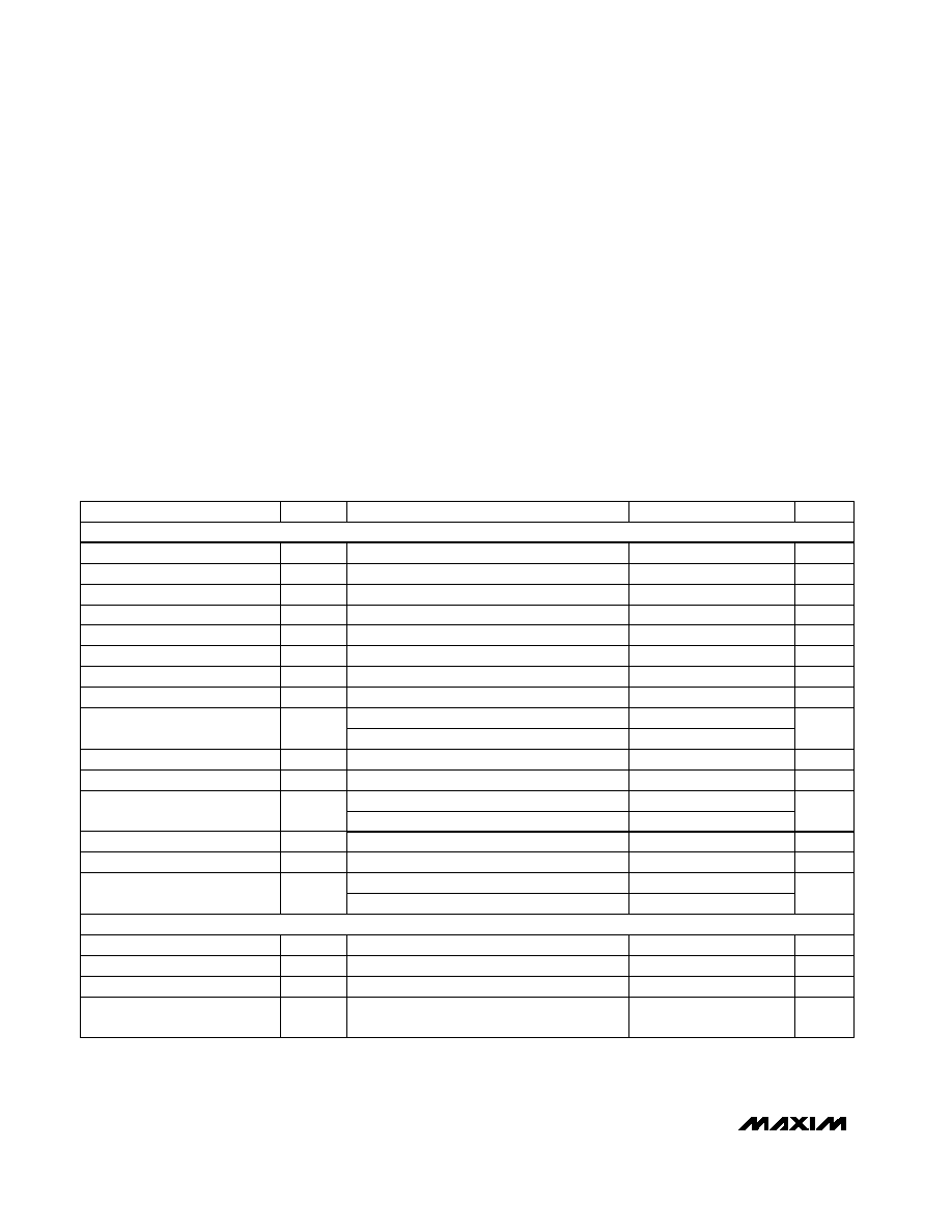
10
9
8
7
6
1
2
3
4
5
GND
V
DD
RFB
INV
DIN
SCLK
CS
REF
TOP VIEW
MAX5142
MAX5144
OUT
CLR
µMAX
OUT
SCLK
CS
1
2
8
7 V
DD
DIN
REF
MAX5141
MAX5143
3
4
6
5
µMAX
GND
CLR
Pin Configurations
MAX5141MAX5144
+3V/+5V, Serial-Input,
Voltage-Output, 14-Bit DACs
2
_______________________________________________________________________________________
ABSOLUTE MAXIMUM RATINGS
ELECTRICAL CHARACTERISTICS
(V
DD
= +3V (MAX5143/MAX5144) or +5V (MAX5141/MAX5142), V
REF
= +2.5V, T
A
= T
MIN
to T
MAX
, C
L
= 10pF, GND = 0, R
L
=
,
unless otherwise noted. Typical values are at T
A
= +25°C.)
Stresses beyond those listed under "Absolute Maximum Ratings" may cause permanent damage to the device. These are stress ratings only, and functional
operation of the device at these or any other conditions beyond those indicated in the operational sections of the specifications is not implied. Exposure to
absolute maximum rating conditions for extended periods may affect device reliability.
V
DD
to GND ..............................................................-0.3V to +6V
CS, SCLK, DIN, CLR to GND ...................................-0.3V to +6V
REF to GND................................................-0.3V to (V
DD
+ 0.3V)
OUT, INV to GND .....................................................-0.3V to V
DD
RFB to INV ...................................................................-6V to +6V
RFB to GND.................................................................-6V to +6V
Maximum Current into Any Pin............................................50mA
Continuous Power Dissipation (T
A
= +70°C)
8-Pin µMAX (derate 4.5mW/°C above +70°C)...............362mW
10-Pin µMAX (derate 5.6mW/°C above +70°C).............444mW
Operating Temperature Ranges
MAX514_ EUA ...................................................-40°C to +85°C
MAX514_ EUB ...................................................-40°C to +85°C
Storage Temperature Range .............................-65°C to +150°C
Maximum Die Temperature..............................................+150°C
Lead Temperature (soldering, 10s) .................................+300°C
REFERENCE INPUT
STATIC PERFORMANCE--ANALOG SECTION
Integral Nonlinearity
INL
LSB
±0.5
±1
MAX514_
+4.5V
V
DD
+5.5V (MAX5141/MAX5142)
±1
Power-Supply Rejection
+2.7V
V
DD
+3.3V (MAX5143/MAX5144)
±1
LSB
Ratio error
%
LSB
R
FB
/R
INV
Digital Feedthrough
nV-s
0.2
Code = 0000 hex; CS = V
DD
;
SCLK, DIN = 0V to V
DD
levels
DAC Glitch Impulse
nV-s
7
Major-carry transition
Output Settling Time
µs
1
To ±
1
/
2
LSB of FS
DYNAMIC PERFORMANCE--ANALOG SECTION
Voltage-Output Slew Rate
SR
V/µs
15
(Note 5)
Bipolar Zero Offset Error
Guaranteed monotonic
LSB
ZSE
PARAMETER
SYMBOL
MIN
TYP
MAX
UNITS
Zero-Code Offset Error
±2
Differential Nonlinearity
DNL
LSB
Zero-Code Tempco
ZS
TC
±0.05
ppm/°C
±10
Gain Error (Note 1)
LSB
Gain-Error Tempco
±0.1
ppm/°C
Resolution
N
14
Bits
±0.5
±1
6.2
k
DAC Output Resistance
R
OUT
1
Bipolar Resistor Matching
±0.03
±20
Bipolar Zero Tempco
BZS
TC
±0.5
ppm/°C
PSR
Reference Input Range
V
REF
2.0
V
DD
V
10
Reference Input Resistance
(Note 4)
R
REF
6
k
CONDITIONS
(Note 2)
(Note 3)
Unipolar mode
Bipolar mode
STATIC PERFORMANCE--ANALOG SECTION
MAX5141MAX5144
+3V/+5V, Serial-Input,
Voltage-Output, 14-Bit DACs
_______________________________________________________________________________________
3
TIMING CHARACTERISTICS
(V
DD
= +2.7V to +3.3V (MAX5143/MAX5144), V
DD
= +4.5V to +5.5V (MAX5141/MAX5142), V
REF
= +2.5V, GND = 0, CMOS inputs,
T
A
= T
MIN
to T
MAX
, unless otherwise noted. Typical values are at T
A
= +25°C.) (Figure 1)
Note 1: Gain error tested at V
REF
= +2.0V, +2.5V, and +3.0V (MAX5143/MAX5144) or V
REF
= +2.0V, +2.5V, +3.0V, and +5.0V
(MAX5141/MAX5142).
Note 2: R
OUT
tolerance is typically ±20%.
Note 3: Min/max range guaranteed by gain-error test. Operation outside min/max limits will result in degraded performance.
Note 4: Reference input resistance is code dependent, minimum at 2155 hex in unipolar mode, 1155 hex in bipolar mode.
Note 5: Slew-rate value is measured from 10% to 90%.
Note 6: Guaranteed by design. Not production tested.
Note 7: Guaranteed by power-supply rejection test and Timing Characteristics.
Code = 3FFF hex
All digital inputs at
V
DD
or GND
All digital inputs at V
DD
or GND
MAX5143/MAX5144
Code = 0000 hex, V
REF
= 1V
P-P
at 100kHz
Code = 0000 hex
Code = 3FFF hex
(Note 6)
CONDITIONS
mW
0.36
PD
Power Dissipation
mA
0.12
0.20
I
DD
Positive Supply Current
V
2.7
3.6
V
DD
Positive Supply Range (Note 7)
V
0.15
V
H
Hysteresis Voltage
pF
3
10
C
IN
Input Capacitance
mV
P-P
1
MHz
1
BW
Reference -3dB Bandwidth
µA
±1
I
IN
Input Current
V
0.8
V
IL
Input Low Voltage
V
2.4
V
IH
Input High Voltage
Reference Feedthrough
dB
92
SNR
Signal-to-Noise Ratio
70
pF
170
C
INREF
Reference Input Capacitance
UNITS
MIN
TYP
MAX
SYMBOL
PARAMETER
(Note 6)
CONDITIONS
µs
20
V
DD
High to CS Low
(Power-Up Delay)
ns
20
t
CL
SCLK Pulse Width Low
ns
20
t
CH
MHz
25
f
CLK
SCLK Frequency
SCLK Pulse Width High
ns
20
t
CLW
CLR Pulse Width Low
ns
0
t
DH
DIN to SCLK High Hold
ns
15
t
DS
DIN to SCLK High Setup
ns
15
t
CSS0
CS Low to SCLK High Setup
ns
15
t
CSS1
CS High to SCLK High Setup
ns
35
t
CSH0
SCLK High to CS Low Hold
ns
20
t
CSH1
SCLK High to CS High Hold
UNITS
MIN
TYP
MAX
SYMBOL
PARAMETER
ELECTRICAL CHARACTERISTICS (continued)
(V
DD
= +3V (MAX5143/MAX5144) or +5V (MAX5141/MAX5142), V
REF
= +2.5V, T
A
= T
MIN
to T
MAX
, C
L
= 10pF, GND = 0, RL =
,
unless otherwise noted. Typical values are at T
A
= +25°C.)
0.60
MAX5141/MAX5142
MAX5143/MAX5144
MAX5141/MAX5142
4.5
5.5
DYNAMIC PERFORMANCE--REFERENCE SECTION
STATIC PERFORMANCE--DIGITAL INPUTS
POWER SUPPLY
MAX5141MAX5144
+3V/+5V, Serial-Input, Voltage-Output, 14-Bit
DACs
4
_______________________________________________________________________________________
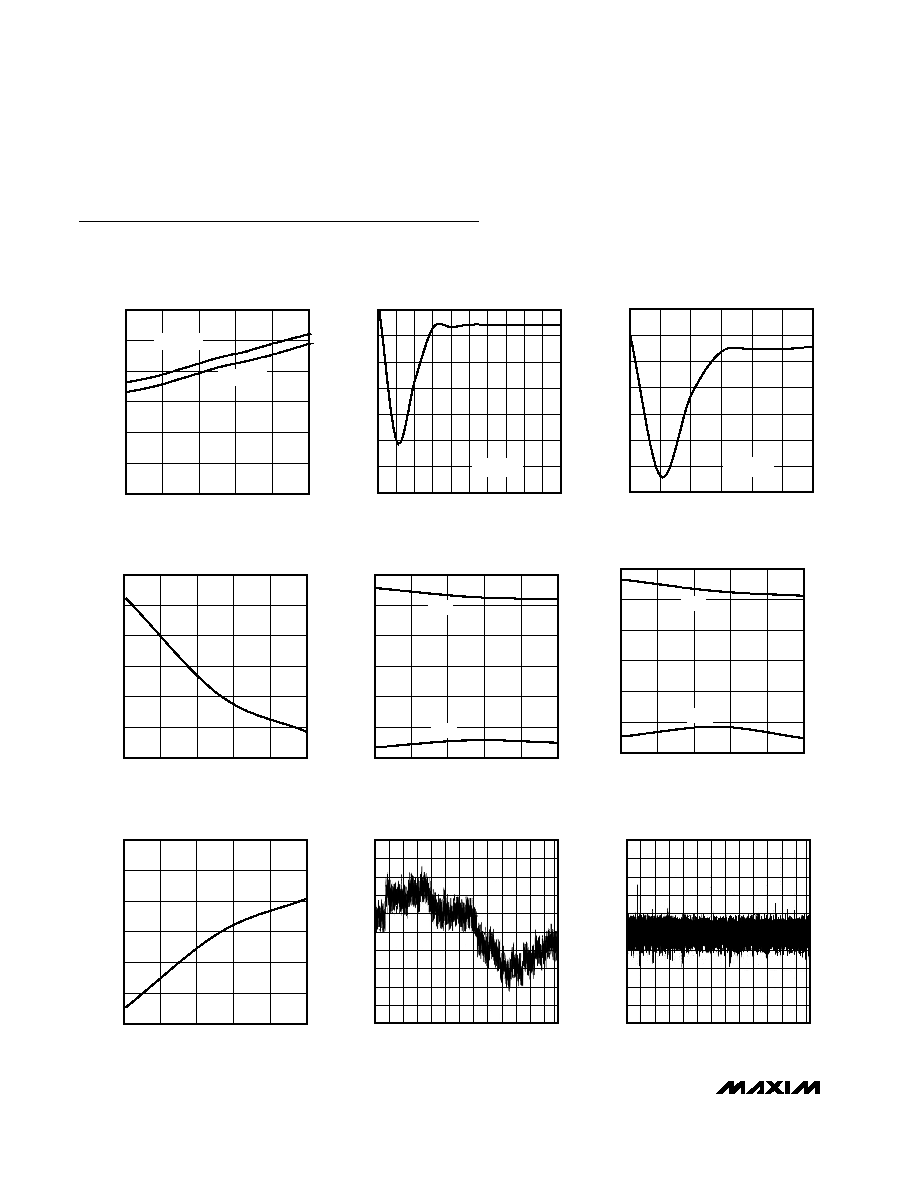
Typical Operating Characteristics
(V
DD
= +3V (MAX5143/MAX5144) or +5V (MAX5141/MAX5142), V
REF
= +2.5V, T
A
= T
MIN
to T
MAX
, GND = 0, R
L
=
, unless otherwise
noted. Typical values are at T
A
= +25°C.)
0
0.050
0.025
0.100
0.075
0.125
0.150
-40
10
-15
35
60
85
SUPPLY CURRENT vs. TEMPERATURE
MAX5141/44 toc01
TEMPERATURE (
°C)
SUPPLY CURRENT (mA)
V
DD
= +5V
V
DD
= +3V
0.05
0.07
0.06
0.09
0.08
0.11
0.10
0.12
0
1.0 1.5
0.5
2.0 2.5 3.0 3.5
4.5 5.0
SUPPLY CURRENT
vs. REFERENCE VOLTAGE
MAX5141/44 toc02
REFERENCE VOLTAGE (V)
SUPPLY CURRENT (mA)
4.0
V
DD
= +5V
0
1.0
1.5
0.5
2.0
2.5
3.0
0.05
0.07
0.06
0.09
0.08
0.11
0.10
0.12
SUPPLY CURRENT
vs. REFERENCE VOLTAGE
MAX5141/44 toc03
REFERENCE VOLTAGE (V)
SUPPLY CURRENT (mA)
V
DD
= +3V
-0.2
0
-0.1
0.2
0.1
0.3
0.4
-40
10
-15
35
60
85
ZERO-CODE OFFSET ERROR
vs. TEMPERATURE
MAX5141 toc04
TEMPERATURE (
°C)
OFFSET ERROR (LSB)
-0.30
-0.20
-0.25
-0.10
-0.15
-0.05
0
-40
10
-15
35
60
85
GAIN ERROR vs. TEMPERATURE
MAX5141 toc07
TEMPERATURE (
°C)
GAIN ERROR (LSB)
0.5
0.4
0.3
0.2
0.1
0.0
-0.1
-0.2
-0.3
-0.4
-0.5
0
2.50k 5.00k 7.50k 10.00k 12.50k 15.00k
DIFFERENTIAL NONLINEARITY vs. CODE
MAX5141 toc08
DNL (LSB)
CODE
1.0
0.8
0.6
0.4
0.2
0.0
-0.2
-0.4
-0.6
-0.8
-1.0
CODE
0
2.50k 5.00k 7.50k 10.00k 12.50k 15.00k
INTEGRAL NONLINEARITY vs. CODE
MAX5141 toc09
INL (LSB)
-0.4
0
-0.2
0.4
0.2
0.6
0.8
-40
10
-15
35
60
85
INTEGRAL NONLINEARITY
vs. TEMPERATURE
MAX5141 toc05
TEMPERATURE (
°C)
INL (LSB)
+INL
-INL
-0.4
-0.2
-0.3
0
-0.1
0.1
0.2
-40
10
-15
35
60
85
DIFFERENTIAL NONLINEARITY
vs. TEMPERATURE
MAX5141 toc06
TEMPERATURE (
°C)
DNL (LSB)
+DNL
-DNL
MAX5141MAX5144
+3V/+5V, Serial-Input,
Voltage-Output, 14-Bit DACs
_______________________________________________________________________________________
5
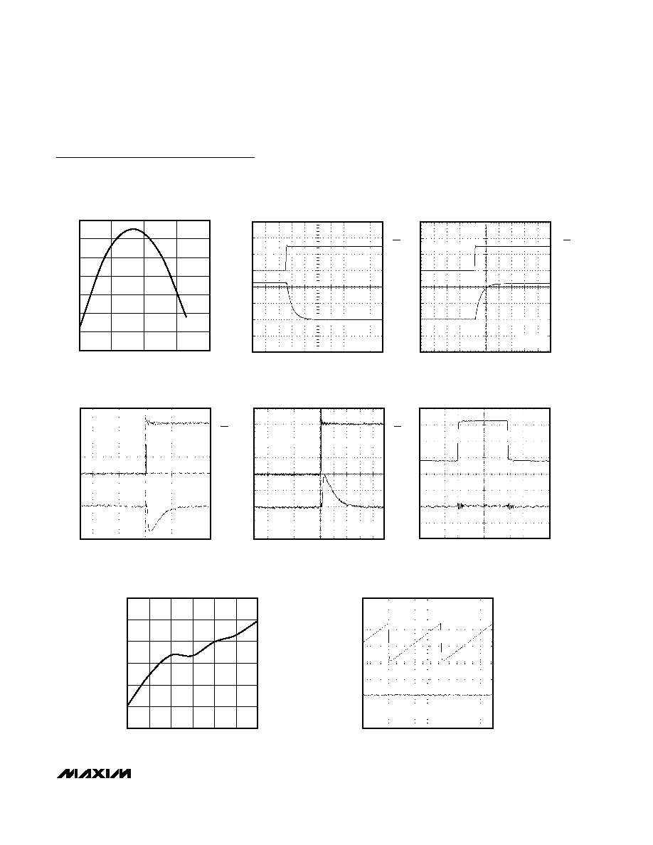
FULL-SCALE STEP RESPONSE
(FALLING)
MAX5141/44 toc11
400ns/div
CS
2V/div
A
OUT
2V/div
C
L
= 20pF
FULL-SCALE STEP RESPONSE
(RISING)
MAX5141/44 toc12
400ns/div
CS
2V/div
A
OUT
2V/div
C
L
= 20pF
MAJOR-CARRY GLITCH
(RISING)
MAX5141/44 toc13
200ns/div
CS
1V/div
A
OUT
20mV/div
C
L
= 20pF
0.40
0.50
0.45
0.60
0.55
0.65
0.70
2.0
3.0
3.5
2.5
4.0
4.5
5.0
INTEGRAL NONLINEARITY vs.
REFERENCE VOLTAGE
MAX5141 toc16
REFERENCE VOLTAGE (V)
INL (LSB)
MAJOR-CARRY GLITCH
(FALLING)
MAX5141/44 toc14
200ns/div
CS
1V/div
A
OUT
20mV/div
C
L
= 20pF
DIGITAL FEEDTHROUGH
MAX5141/44 toc15
50ns/div
D
IN
2V/div
A
OUT
10mV/div
0
40
20
80
60
120
100
140
REFERENCE CURRENT
vs. DIGITAL INPUT CODE
MAX5141 toc10
INPUT CODE
REFERENCE CURRENT (
µ
A)
0
5k
10k
15k
20k
Typical Operating Characteristics (continued)
(V
DD
= +3V (MAX5143/MAX5144) or +5V (MAX5141/MAX5142), V
REF
= +2.5V, T
A
= T
MIN
to T
MAX
, GND = 0, R
L
=
, unless otherwise
noted. Typical values are at T
A
= +25°C.)
UNIPOLAR POWER-ON GLITCH
(REF = V
DD
)
MAX5141/44 toc17
50ms/div
V
DD
2V/div
V
OUT
10mV/div