 | –≠–ª–µ–∫—Ç—Ä–æ–Ω–Ω—ã–π –∫–æ–º–ø–æ–Ω–µ–Ω—Ç: MAX5152 | –°–∫–∞—á–∞—Ç—å:  PDF PDF  ZIP ZIP |
For free samples & the latest literature: http://www.maxim-ic.com, or phone 1-800-998-8800.
For small orders, phone 408-737-7600 ext. 3468.
MAX5152/MAX5153
Low-Power, Dual, 13-Bit Voltage-Output DACs
with Configurable Outputs
________________________________________________________________
Maxim Integrated Products
1
19-1304; Rev 0; 10/97
_______________General Description
The MAX5152/MAX5153 low-power, serial, voltage-out-
put, dual 13-bit digital-to-analog converters (DACs)
consume only 500µA from a single +5V (MAX5152) or
+3V (MAX5153) supply. These devices feature Rail-to-
Rail
Æ
output swing and are available in space-saving
16-pin QSOP and DIP packages. Access to the invert-
ing input allows for specific gain configurations, remote
sensing, and high output current capability, making
these devices ideally suited for industrial process con-
trols. These devices are also well suited for digitally
programmable (4≠20mA) current loops.
The 3-wire serial interface is SPITM/QSPITM and
MicrowireTM compatible. Each DAC has a double-
buffered input organized as an input register followed
by a DAC register, which allows the input and DAC reg-
isters to be updated independently or simultaneously.
Additional features include a programmable shutdown
(2µA), hardware-shutdown lockout, a separate voltage
reference for each DAC, power-on reset, and an active-
low clear input (CL) that resets all registers and DACs
to zero. The MAX5152/MAX5153 provide a programma-
ble logic output pin for added functionality, and a seri-
al-data output pin for daisy chaining.
________________________Applications
Industrial Process Control
Motion Control
Digital Offset and Gain
Digitally Programmable
Adjustment
4≠20mA Current Loops
Remote Industrial Controls
Automatic Test Equipment
____________________________Features
o
13-Bit Dual DAC with Configurable Output
Amplifier
o
Single-Supply Operation: +5V (MAX5152)
+3V (MAX5153)
o
Rail-to-Rail Output Swing
o
Low Quiescent Current:
500µA (normal operation)
2µA (shutdown mode)
o
Power-On Reset Clears DAC Outputs to Zero
o
SPI/QSPI and Microwire Compatible
o
Space-Saving 16-Pin QSOP Package
o
Pin-Compatible 12-Bit Versions:
MAX5156/MAX5157
______________Ordering Information
Rail-to-Rail is a registered trademark of Nippon Motorola Ltd. SPI and QSPI are trademarks of Motorola, Inc.
Microwire is a trademark of National Semiconductor Corp.
Ordering Information continued at end of data sheet.
*
Dice are tested at T
A
= +25∞C, DC parameters only.
Dice*
0∞C to +70∞C
±1
MAX5152BC/D
16 QSOP
0∞C to +70∞C
±1
MAX5152BCEE
16 QSOP
0∞C to +70∞C
±1/2
MAX5152ACEE
16 Plastic DIP
0∞C to +70∞C
±1
MAX5152BCPE
16 Plastic DIP
0∞C to +70∞C
±1/2
MAX5152
ACPE
PIN-PACKAGE
TEMP. RANGE
INL
(LSB)
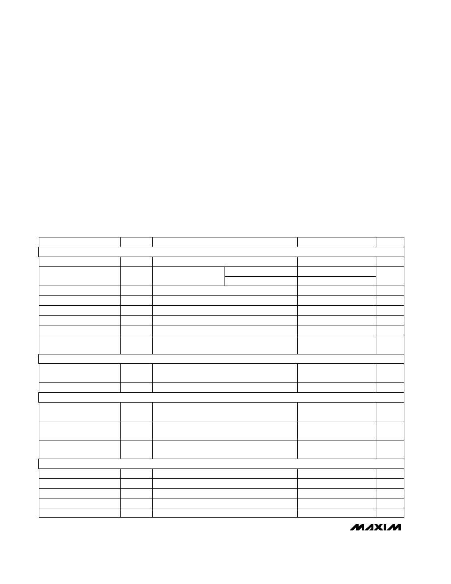
PART
REFA
CL
DOUT
16-BIT
SHIFT
REGISTER
SR
CONTROL
INPUT
REG A
SCLK UPO
REFB
DIN
CS
DAC A
DAC B
FBA
FBB
OUTA
OUTB
DAC
REG A
INPUT
REG B
LOGIC
OUTPUT
DECODE
CONTROL
DAC
REG B
MAX5152
MAX5153
V
DD
AGND
DGND
PDL
_________________________________________________________Functional Diagram
Pin Configuration appears at end of data sheet.
MAX5152/MAX5153
Low-Power, Dual, 13-Bit Voltage-Output DACs
with Configurable Outputs
2
_______________________________________________________________________________________
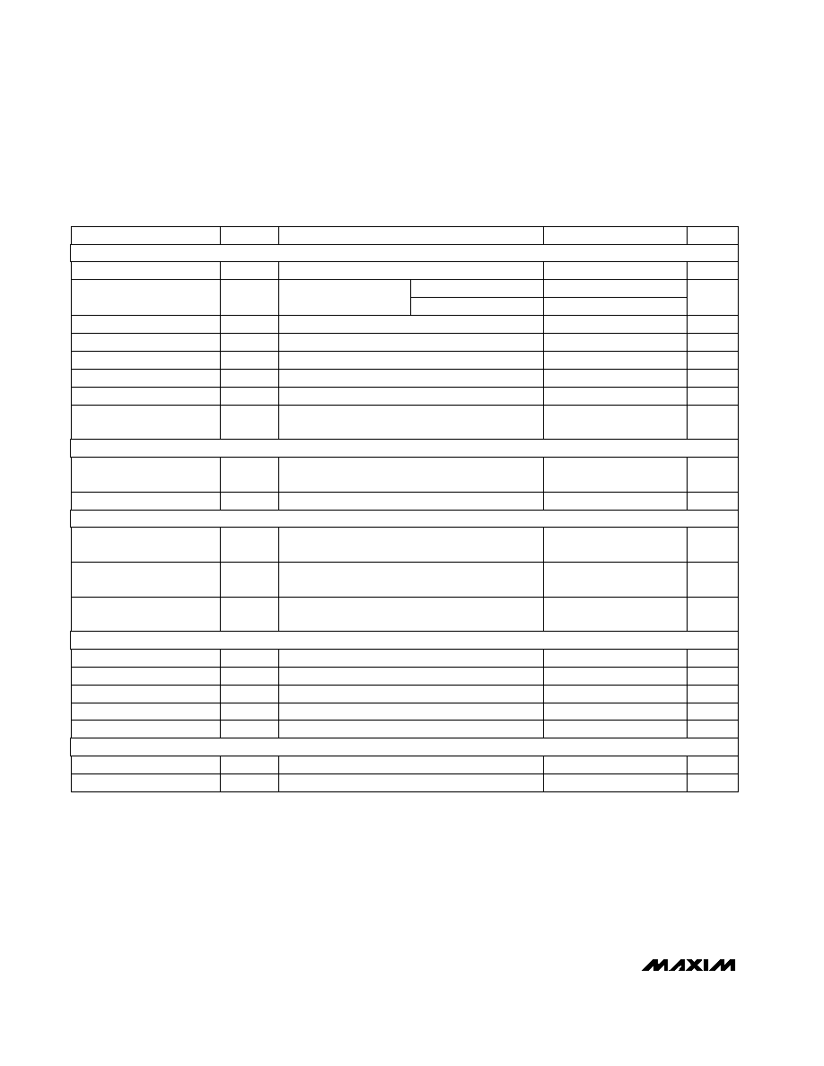
ABSOLUTE MAXIMUM RATINGS
ELECTRICAL CHARACTERISTICS--MAX5152
(V
DD
= +5V ±10%, V
REFA
= V
REFB
= 2.5V, R
L
= 10k
, C
L
= 100pF, T
A
= T
MIN
to T
MAX
, unless otherwise noted. Typical values are at
T
A
= +25∞C, output buffer connected in unity-gain configuration (Figure 9).)
Stresses beyond those listed under "Absolute Maximum Ratings" may cause permanent damage to the device. These are stress ratings only, and functional
operation of the device at these or any other conditions beyond those indicated in the operational sections of the specifications is not implied. Exposure to
absolute maximum rating conditions for extended periods may affect device reliability.
V
DD
to AGND............................................................-0.3V to +6V
V
DD
to DGND ...........................................................-0.3V to +6V
AGND to DGND ..................................................................±0.3V
FBA, FBB to AGND.....................................-0.3V to (V
DD
+ 0.3V)
REF_, OUT_ to AGND.................................-0.3V to (V
DD
+ 0.3V)
Digital Inputs (SCLK, DIN, CS, CL, PDL)
to DGND ................................................................-0.3V to +6V
Digital Outputs (DOUT, UPO) to DGND .....-0.3V to (V
DD
+ 0.3V)
Maximum Current into Any Pin .........................................±20mA
Continuous Power Dissipation (T
A
= +70∞C)
Plastic DIP (derate 10.5mW/∞C above +70∞C) .............593mW
QSOP (derate 8.30mW/∞C above +70∞C) .....................667mW
CERDIP (derate 10.00mW/∞C above +70∞C) ................800mW
Operating Temperature Ranges
MAX5152_C_E/MAX5153_C_E ...........................0∞C to +70∞C
MAX5152_E_E/MAX5153_E_E..........................-40∞C to +85∞C
MAX5152_MJE/MAX5153_MJE ......................-55∞C to +125∞C
Storage Temperature Range .............................-65∞C to +150∞C
Lead Temperature (soldering, 10sec) .............................+300∞C
V
IN
= 0V to V
DD
CL, PDL, CS, DIN, SCLK
CL, PDL, CS, DIN, SCLK
Input code = 1FFF hex,
V
REF
= 1Vp-p at 2.5V
DC
, f = 25kHz
Input code = 0000 hex,
V
REF
= (V
DD
- 1.4Vp-p) at 1kHz
4.5V
V
DD
5.5V
Input code = 1FFF hex,
V
REF
= 0.67Vp-p at 2.5V
DC
Normalized to 2.5V
(Note 1)
Guaranteed monotonic
Code = 20
Minimum with code 1555 hex
Normalized to 2.5V
CONDITIONS
pF
8
C
IN
Input Capacitance
µA
0.001
±1
I
IN
Input Leakage Current
mV
200
V
HYS
Input Hysteresis
V
0.8
V
IL
Input Low Voltage
V
3.0
V
IH
Input High Voltage
dB
82
SINAD
Signal-to-Noise plus
Distortion Ratio
dB
-85
Reference Feedthrough
kHz
600
Reference 3dB Bandwidth
k
14
20
R
REF
Reference Input Resistance
V
0
V
DD
-
1.4
REF
Reference Input Range
±1/2
Bits
13
N
Resolution
µV/V
20
200
PSRR
V
DD
Power-Supply
Rejection Ratio
ppm/∞C
3
Gain-Error Tempco
LSB
-0.5
±6
Gain Error
LSB
±1
INL
Integral Nonlinearity
LSB
±1
DNL
Differential Nonlinearity
mV
±6
V
OS
Offset Error
ppm/∞C
3
TCV
OS
Offset Tempco
UNITS
MIN
TYP
MAX
SYMBOL
PARAMETER
MAX5152A
MAX5152B
STATIC PERFORMANCE
REFERENCE INPUT
MULTIPLYING-MODE PERFORMANCE
DIGITAL INPUTS

MAX5152/MAX5153
Low-Power, Dual, 13-Bit Voltage-Output DACs
with Configurable Outputs
_______________________________________________________________________________________
3
ELECTRICAL CHARACTERISTICS--MAX5152 (continued)
(V
DD
= +5V ±10%, V
REFA
= V
REFB
= 2.5V, R
L
= 10k
, C
L
= 100pF, T
A
= T
MIN
to T
MAX
, unless otherwise noted. Typical values are at
T
A
= +25∞C, output buffer connected in unity-gain configuration (Figure 9).)
Note 1:
Accuracy is specified from code 20 to code 8191.
Note 2:
Accuracy is better than 1LSB for V
OUT
greater than 6mV and less than V
DD
- 50mV. Guaranteed by PSRR test at the end
points.
Note 3:
Digital inputs are set to either V
DD
or DGND, code = 0000 hex, R
L
=
.
Note 4:
SCLK minimum clock period includes rise and fall times.
CS = V
DD
, f
DIN
= 100kHz, V
SCLK
= 5Vp-p
I
SOURCE
= 2mA
Rail-to-rail (Note 2)
To 1/2LSB of full-scale, V
STEP
= 2.5V
I
SINK
= 2mA
CONDITIONS
nV-s
5
Digital Crosstalk
nV-s
5
Digital Feedthrough
µs
25
Time Required to Exit
Shutdown
µA
0
±0.1
I
FB
_
Current into FBA or FBB
V
V
DD
-
0.5
V
OH
Output High Voltage
V
0 to V
DD
Output Voltage Swing
µs
20
Output Settling Time
V
0.13
0.40
V
OL
Output Low Voltage
V/µs
0.75
SR
Voltage Output Slew Rate
UNITS
MIN
TYP
MAX
SYMBOL
PARAMETER
(Note 4)
(Note 3)
(Note 3)
ns
40
t
CL
SCLK Pulse Width Low
ns
40
t
CH
SCLK Pulse Width High
ns
100
t
CP
SCLK Clock Period
µA
±1
Reference Current in
Shutdown
µA
2
10
I
DD(SHDN)
Power-Supply Current in
Shutdown
mA
0.5
0.65
I
DD
Power-Supply Current
V
4.5
5.5
V
DD
Positive Supply Voltage
ns
40
t
DS
DIN Setup Time
ns
0
t
CHS
SCLK Rise to CS Rise Hold
Time
ns
40
t
CSS
CS Fall to SCLK Rise Setup
Time
C
LOAD
= 200pF
C
LOAD
= 200pF
ns
80
t
DO2
SCLK Fall to DOUT Valid
Propagation Delay
ns
80
t
DO1
SCLK Rise to DOUT Valid
Propagation Delay
ns
0
t
DH
DIN Hold Time
ns
100
t
CSW
CS Pulse Width High
ns
40
t
CS1
CS Rise to SCLK Rise Hold
ns
10
t
CS0
SCLK Rise to CS Fall Delay
DIGITAL OUTPUTS (DOUT, UPO)
DYNAMIC PERFORMANCE
POWER SUPPLIES
TIMING CHARACTERISTICS
MAX5152/MAX5153
Low-Power, Dual, 13-Bit Voltage-Output DACs
with Configurable Outputs
4
_______________________________________________________________________________________
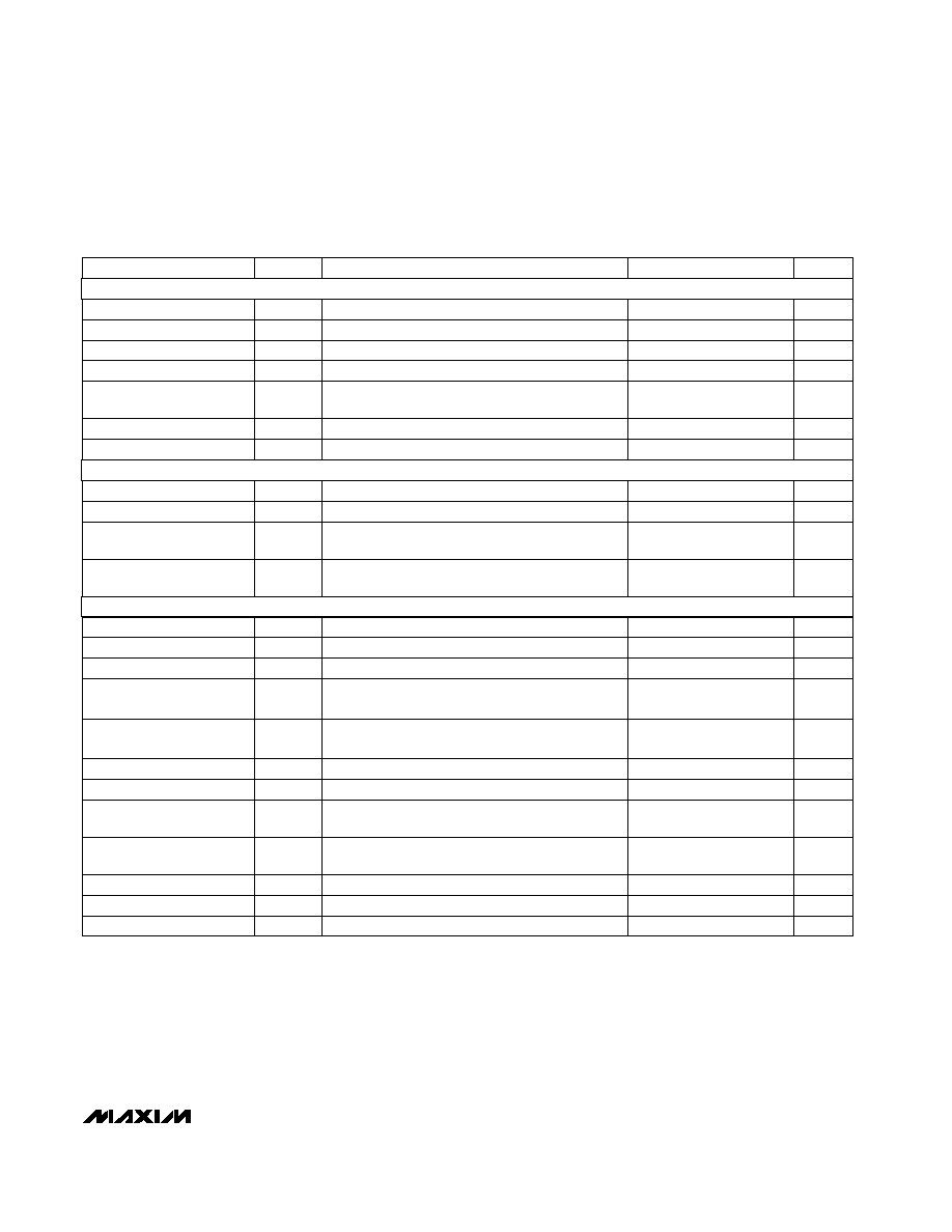
ELECTRICAL CHARACTERISTICS--MAX5153
(V
DD
= +2.7V to +3.6V, V
REFA
= V
REFB
= 1.25V, R
L
= 10k
, C
L
= 100pF, T
A
= T
MIN
to T
MAX
, unless otherwise noted. Typical values
are at T
A
= +25∞C, output buffer connected in unity-gain configuration (Figure 9).)
V
IN
= 0V to V
DD
CL, PDL, CS, DIN, SCLK
CL, PDL, CS, DIN, SCLK
Input code = 1FFF hex,
V
REF
= 1Vp-p at 1.25V
DC
, f = 15kHz
Input code = 0000 hex,
V
REF
= (V
DD
- 1.4V) at 1kHz
2.7V
V
DD
3.6V
Input code = 1FFF hex,
V
REF(AC)
= 0.67Vp-p at 1.25V
DC
Normalized to 1.25V
(Note 5)
Guaranteed monotonic
Code = 40
Minimum with code 1555 hex
Normalized to 1.25V
CONDITIONS
pF
8
C
IN
Input Capacitance
µA
0
±0.1
I
IN
Input Leakage Current
mV
200
V
HYS
Input Hysteresis
V
0.8
V
IL
Input Low Voltage
V
2.2
V
IH
Input High Voltage
dB
73
SINAD
Signal-to-Noise plus
Distortion Ratio
dB
-92
Reference Feedthrough
kHz
600
Reference 3dB Bandwidth
k
14
R
REF
Reference Input Resistance
V
0
V
DD
-
1.4
REF
Reference Input Range
±1
Bits
13
N
Resolution
µV/V
20
320
PSRR
V
DD
Power-Supply
Rejection Ratio
ppm/∞C
6
Gain-Error Tempco
LSB
-0.5
±8
Gain Error
LSB
±2
INL
Integral Nonlinearity
LSB
±1
DNL
Differential Nonlinearity
mV
±6
V
OS
Offset Error
ppm/∞C
6
TCV
OS
Offset Tempco
UNITS
MIN
TYP
MAX
SYMBOL
PARAMETER
MAX5153A
MAX5153B
I
SINK
= 2mA
I
SOURCE
= 2mA
V
0.13
0.4
V
OL
Output Low Voltage
V
V
DD
- 0.5
V
OH
Output High Voltage
STATIC PERFORMANCE
REFERENCE INPUT (V
REF
)
MULTIPLYING-MODE PERFORMANCE
DIGITAL INPUTS
DIGITAL OUTPUTS (DOUT, UPO)
MAX5152/MAX5153
Low-Power, Dual, 13-Bit Voltage-Output DACs
with Configurable Outputs
_______________________________________________________________________________________
5
ELECTRICAL CHARACTERISTICS--MAX5153 (continued)
(V
DD
= +2.7V to +3.6V, V
REFA
= V
REFB
= 1.25V, R
L
= 10k
, C
L
= 100pF, T
A
= T
MIN
to T
MAX
, unless otherwise noted. Typical values
are at T
A
= +25∞C, output buffer connected in unity-gain configuration (Figure 9).)
CS = V
DD
, f
DIN
= 100kHz, V
SCLK
= 3Vp-p
(Note 4)
(Note 7)
(Note 7)
ns
Rail-to-rail (Note 6)
To 1/2LSB of full-scale, V
STEP
= 1.25V
40
t
CL
SCLK Pulse Width Low
CONDITIONS
ns
40
t
CH
SCLK Pulse Width High
nV-s
5
Digital Crosstalk
nV-s
5
Digital Feedthrough
µs
25
Time Required to Exit
Shutdown
µA
0
±0.1
I
FB_
Current into FBA or FBB
ns
100
t
CP
SCLK Clock Period
µA
±1
Reference Current in
Shutdown
µA
1
8
I
DD(SHDN)
Power-Supply Current in
Shutdown
mA
0.5
0.6
I
DD
Power-Supply Current
V
2.7
3.6
V
DD
Positive Supply Voltage
ns
50
t
DS
DIN Setup Time
ns
0
t
CHS
SCLK Rise to CS Rise Hold
Time
ns
40
t
CSS
CS Fall to SCLK Rise Setup
Time
C
LOAD
= 200pF
V
0 to V
DD
Output Voltage Swing
µs
25
Output Settling Time
C
LOAD
= 200pF
ns
120
V/µs
0.75
SR
Voltage Output Slew Rate
UNITS
MIN
TYP
MAX
SYMBOL
PARAMETER
t
DO2
SCLK Fall to DOUT Valid
Propagation Delay
ns
120
t
DO1
SCLK Rise to DOUT Valid
Propagation Delay
ns
0
t
DH
DIN Hold Time
ns
100
t
CSW
CS Pulse Width High
ns
40
t
CS1
CS Rise to SCLK Rise Hold
ns
10
t
CS0
SCLK Rise to CS Fall Delay
Note 4:
SCLK minimum clock period includes rise and fall times.
Note 5:
Accuracy is specified from code 40 to code 8191.
Note 6:
Accuracy is better than 1LSB for V
OUT
greater than 6mV and less than V
DD
- 100mV. Guaranteed by PSRR test at the end
points.
Note 7:
Digital inputs are set to either V
DD
or DGND, code = 0000 hex, R
L
=
.
DYNAMIC PERFORMANCE
POWER SUPPLIES
TIMING CHARACTERISTICS