 | ÐлекÑÑоннÑй компоненÑ: MAX5171 | СкаÑаÑÑ:  PDF PDF  ZIP ZIP |
Äîêóìåíòàöèÿ è îïèñàíèÿ www.docs.chipfind.ru
General Description
The MAX5171/MAX5173 low-power, serial, voltage-output,
14-bit digital-to-analog converters (DACs) feature a preci-
sion output amplifier in a space-saving 16-pin QSOP
package. The MAX5171 operates from a +5V single sup-
ply, and the MAX5173 operates from a +3V single supply.
The output amplifier's inverting input is available to allow
specific gain configurations, remote sensing, and high
output current capability. This makes the MAX5171/
MAX5173 ideal for a wide range of applications, including
industrial process control. Both devices draw only 260µA
of supply current, which reduces to 1µA in shutdown
mode. In addition, the programmable power-up reset fea-
ture allows for a user-selectable output voltage of either 0
or midscale.
The 3-wire serial interface is compatible with SPITM,
QSPITM, and MICROWIRETM standards. An input register
followed by a DAC register provides a double-buffered
input, allowing the input and DAC registers to be updated
independently or simultaneously with a 16-bit serial word.
Additional features include software and hardware shut-
down, shutdown lockout, a hardware clear pin, and a ref-
erence input capable of accepting DC and offset AC
signals. These devices provide a programmable digital
output pin for added functionality and a serial-data output
pin for daisy-chaining. All logic inputs are TTL/CMOS-
compatible and are internally buffered with Schmitt trig-
gers to allow direct interfacing to optocouplers.
The MAX5171/MAX5173 incorporate a proprietary on-chip
circuit that keeps the output voltage virtually "glitch free,"
limiting the glitches to a few millivolts during power-up.
Both devices are available in 16-pin QSOP packages and
are specified for the extended (-40°C to +85°C) tempera-
ture range. The MAX5171/MAX5173 are pin-compatible
upgrades to the 12-bit MAX5175/MAX5177. For 100% pin-
compatible DACs with an internal reference, see the 13-bit
MAX5132/MAX5133 and the 12-bit MAX5122/MAX5123
data sheets.
Applications
Features
o
±1 LSB INL
o
1µA Shutdown Current
o
"Glitch Free" Output Voltage at Power-Up
o
Single-Supply Operation: +5V (MAX5171)
+3V (MAX5173)
o
Full-Scale Output Range:
+2.048V (MAX5173, V
REF
= +1.25V)
+4.096V (MAX5171, V
REF
= +2.5V )
o
Rail-to-Rail
®
Output Amplifier
o
Low THD (-80dB) in Multiplying Operation
o
SPI/QSPI/MICROWIRE-Compatible 3-Wire
Serial Interface
o
Programmable Shutdown Mode and Power-Up
Reset
o
Buffered Output Capable of Driving 5k
|| 100pF
Loads
o
User-Programmable Digital Output Pin Allows
Serial Control of External Components
o
Pin-Compatible Upgrade to the 12-Bit
MAX5175/MAX5177
For free samples & the latest literature: http://www.maxim-ic.com, or phone 1-800-998-8800.
For small orders, phone 1-800-835-8769.
MAX5171/MAX5173
Low-Power, Serial, 14-Bit DACs
with Force/Sense Voltage Output
________________________________________________________________
Maxim Integrated Products
1
19-1476; Rev 0; 4/99
Pin Configuration
Functional Diagram appears at end of data sheet.
16
15
14
13
12
11
10
9
1
2
3
4
5
6
7
8
FB
V
DD
N.C.
REF
AGND
PDL
UPO
DOUT
DGND
TOP VIEW
MAX5171
MAX5173
QSOP
OUT
RS
CS
SHDN
CLR
DIN
SCLK
Ordering Information
Digitally Programmable 420mA Current Loops
Industrial Process Control
Digital Offset and Gain Adjustment
Motion Control
Automatic Test Equipment (ATE)
Remote Industrial Controls
µP-Controlled Systems
SPI and QSPI are trademarks of Motorola, Inc.
MICROWIRE is a trademark of National Semiconductor Corp.
Rail-to-Rail is a registered trademark of Nippon Motorola, Ltd.
PART
MAX5171
AEEE
MAX5171BEEE
MAX5173
AEEE
-40°C to +85°C
-40°C to +85°C
-40°C to +85°C
TEMP. RANGE
PIN-PACKAGE
16 QSOP
16 QSOP
16 QSOP
MAX5173BEEE
-40°C to +85°C
16 QSOP
INL
(LSB)
±1
±2
±2
±4
MAX5171/MAX5173
Low-Power, Serial, 14-Bit DACs
with Force/Sense Voltage Output
2
_______________________________________________________________________________________
ABSOLUTE MAXIMUM RATINGS
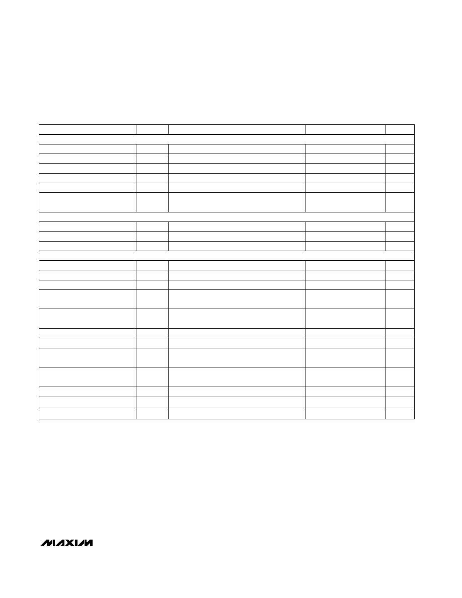
ELECTRICAL CHARACTERISTICS--MAX5171
(V
DD
= +5.0V ±10%, V
REF
= +2.5V, AGND = DGND, FB = OUT, R
L
= 5k
, C
L
= 100pF referenced to ground, T
A
= T
MIN
to T
MAX,
unless otherwise noted. Typical values are at T
A
= +25°C.)
Stresses beyond those listed under "Absolute Maximum Ratings" may cause permanent damage to the device. These are stress ratings only, and functional
operation of the device at these or any other conditions beyond those indicated in the operational sections of the specifications is not implied. Exposure to
absolute maximum rating conditions for extended periods may affect device reliability.
V
DD
to AGND, DGND ............................................-0.3V to +6.0V
AGND to DGND.....................................................-0.3V to +0.3V
Digital Inputs to DGND..........................................-0.3V to +6.0V
DOUT, UPO to DGND ................................-0.3V to (V
DD
+ 0.3V)
FB, OUT, REF to AGND .............................-0.3V to (V
DD
+ 0.3V)
Maximum Current into Any Pin............................................50mA
Continuous Power Dissipation (T
A
= +70°C)
16-pin QSOP (derate 8mW/°C above +70°C)..............667mW
Operating Temperature Range ...........................-40°C to +85°C
Storage Temperature Range .............................-65°C to +150°C
Lead Temperature (soldering, 10sec) .............................+300°C
CONDITIONS
UNITS
MIN
TYP
MAX
SYMBOL
PARAMETER
Bits
14
Resolution
MAX5171A
±1
MAX5171B
LSB
±2
INL
Integral Nonlinearity (Note 1)
LSB
±1
DNL
Differential Nonlinearity
mV
±10
V
OS
Offset Error (Note 2)
R
L
=
LSB
-0.6
±4
GE
Gain Error
R
L
= 5k
-1.6
±8
µV/V
10
120
PSRR
Power-Supply Rejection Ratio
f = 100kHz
LSBp-p
1
Output Noise Voltage
nV/
Hz
50
Output Thermal Noise Density
V
0
V
DD
- 1.4
V
REF
Reference Input Range
k
18
R
REF
Reference Input Resistance
V
REF
= 0.5Vp-p + 2.5V
DC
, slew-rate limited
kHz
350
Reference -3dB Bandwidth
V
REF
= 1.4Vp-p + 2.5V
DC
, f = 10kHz,
code = 3FFF hex
dB
84
SINAD
Signal-to-Noise Plus Distortion
Ratio
V
3
V
IH
Input High Voltage
V
0.8
V
IL
Input Low Voltage
mV
200
V
HYS
Input Hysteresis
V
IN
= 0 or V
DD
µA
0.001
±1
I
IN
Input Leakage Current
pF
8
C
IN
Input Capacitance
I
SOURCE
= 2mA
V
V
DD
- 0.5
V
OH
Output High Voltage
I
SINK
= 2mA
V
0.13
0.4
V
OL
Output Low Voltage
V
REF
= 3.6Vp-p + 1.8V
DC
, f = 1kHz,
code = all 0s
dB
-84
Reference Feedthrough
STATIC PERFORMANCE
REFERENCE
MULTIPLYING-MODE PERFORMANCE
DIGITAL INPUTS
DIGITAL OUTPUTS
MAX5171/MAX5173
Low-Power, Serial, 14-Bit DACs
with Force/Sense Voltage Output
_______________________________________________________________________________________
3
ELECTRICAL CHARACTERISTICS--MAX5171 (continued)
(V
DD
= +5V ±10%, V
REF
= +2.5V, AGND = DGND, FB = OUT, R
L
= 5k
, C
L
= 100pF referenced to ground, T
A
= T
MIN
to T
MAX
,
unless otherwise noted. Typical values are at T
A
= +25°C.)
CONDITIONS
V/µs
0.6
SR
Voltage Output Slew Rate
V
0
V
DD
Output Voltage Swing (Note 3)
µA
-0.1
0
0.1
Current into FB
µs
40
Time Required to Exit Shutdown
UNITS
MIN
TYP
MAX
SYMBOL
PARAMETER
CS = V
DD
; f
SCLK
= 100kHz, V
SCLK
= 5Vp-p
nV-s
1
Digital Feedthrough
V
4.5
5.5
V
DD
Positive Supply Voltage
mA
0.26
0.35
I
DD
Power-Supply Current (Note 4)
µA
1
10
Shutdown Current (Note 4)
ns
100
t
CP
SCLK Clock Period
ns
40
t
CH
SCLK Pulse Width High
ns
40
t
CL
SCLK Pulse Width Low
ns
40
t
CSS
CS Fall to SCLK Rise Setup
Time
ns
40
t
DS
SDI Setup Time
ns
0
t
DH
SDI Hold Time
C
LOAD
= 200pF
ns
80
t
DO1
SCLK Rise to DOUT Valid
Propagation Delay
C
LOAD
= 200pF
ns
80
t
DO2
SCLK Fall to DOUT Valid
Propagation Delay
ns
10
t
CS0
SCLK Rise to CS Fall Delay
ns
100
t
CSW
CS Pulse Width High
ns
0
t
CSH
SCLK Rise to CS Rise Hold
Time
ns
40
t
CS1
CS Rise to SCLK Rise Hold Time
To ±0.5LSB, from 10mV to full scale
µs
12
Output Settling Time
DYNAMIC PERFORMANCE
POWER SUPPLIES
TIMING CHARACTERISTICS
MAX5171/MAX5173
Low-Power, Serial, 14-Bit DACs
with Force/Sense Voltage Output
4
_______________________________________________________________________________________
ELECTRICAL CHARACTERISTICS--MAX5173
(V
DD
= +2.7V to +3.6V, V
REF
= 1.25V, AGND = DGND, FB = OUT, R
L
= 5k
, C
L
= 100pF referenced to ground, T
A
= T
MIN
to T
MAX
,
unless otherwise noted. Typical values are at T
A
= +25°C).
Bits
14
Resolution
MAX5173A
±2
V
REF
= 1.6Vp-p + 0.8V
DC
, f = 1kHz,
code = all 0s
dB
MAX5173B
LSB
±4
INL
Integral Nonlinearity (Note 5)
LSB
±1
DNL
Differential Nonlinearity
mV
±10
CONDITIONS
V
OS
Offset Error (Note 2)
R
L
=
LSB
-0.6
±4
GE
Gain Error
R
L
= 5k
-1.6
±8
-84
µV/V
10
120
PSRR
Power-Supply Rejection Ratio
f = 100kHz
LSBp-p
2
Output Noise Voltage
nV/
Hz
50
Output Thermal Noise Density
V
0
V
DD
- 1.4
V
REF
Reference Input Range
k
18
R
REF
Reference Input Resistance
V
REF
= 0.5Vp-p + 1.25V
DC
, slew-rate limited
kHz
350
Reference -3dB Bandwidth
V
REF
= 0.9Vp-p + 1.25V
DC
, f = 10kHz,
code = 3 FFF Hex
dB
78
SINAD
Signal-to-Noise Plus Distortion
Ratio
Reference Feedthrough
V
2.2
V
IH
Input High Voltage
V
0.8
V
IL
Input Low Voltage
mV
200
V
HYS
Input Hysteresis
V
IN
= 0 or V
DD
µA
-1
0.001
±1
I
IN
Input Leakage Current
UNITS
MIN
TYP
MAX
SYMBOL
PARAMETER
pF
8
C
IN
Input Capacitance
I
SOURCE
= 2mA
V
V
DD
- 0.5
V
OH
Output High Voltage
I
SINK
= 2mA
V
0.13
0.4
V
OL
Output Low Voltage
STATIC PERFORMANCE
REFERENCE
MULTIPLYING-MODE PERFORMANCE
DIGITAL INPUTS
DIGITAL OUTPUTS
MAX5171/MAX5173
Low-Power, Serial, 14-Bit DACs
with Force/Sense Voltage Output
_______________________________________________________________________________________
5
Note 1:
INL guaranteed between codes 64 and 16383.
Note 2:
Offset is measured at the code that comes closest to 10mV.
Note 3:
Accuracy is better than 1.0 LSB for V
OUT
= 10mV to V
DD
- 180mV. Guaranteed by PSR test on end points.
Note 4:
R
L
= open and digital inputs are either V
DD
or DGND.
Note 5:
INL guaranteed between codes 128 and 16383.
ELECTRICAL CHARACTERISTICS--MAX5173 (continued)
(V
DD
= +2.7V to +3.6V, V
REF
= 1.25V, AGND = DGND, FB = OUT, R
L
= 5k
, C
L
= 100pF referenced to ground, T
A
= T
MIN
to T
MAX
,
unless otherwise noted. Typical values are at T
A
= +25°C).
µA
1
10
Shutdown Current (Note 4)
ns
150
t
CP
SCLK Clock Period
ns
75
t
CH
SCLK Pulse Width High
ns
75
CONDITIONS
t
CL
SCLK Pulse Width Low
ns
60
t
CSS
CS Fall to SCLK Rise Setup
Time
ns
0
t
CSS
SCLK Rise to CS Rise Hold
Time
ns
60
t
DS
SDI Setup Time
ns
0
t
DH
SDI Hold Time
C
LOAD
= 200pF
ns
200
t
DO1
SCLK Rise to DOUT Valid
Propagation Delay
ns
75
t
CS1
CS Rise to SCLK Rise Hold Time
C
LOAD
= 200pF
ns
200
t
DO2
SCLK Fall to DOUT Valid
Propagation Delay
To ±0.5LSB, from 10mV to full-scale
µs
12
Output Settling Time
ns
10
t
CS0
SCLK Rise to CS Fall Delay
ns
150
t
CSW
CS Pulse Width High
V/µs
0.6
SR
Voltage Output Slew Rate
V
0 V
DD
Output Voltage Swing (Note 3)
µA
-0.1
0
0.1
Current into FB
µs
40
Time Required to Exit Shutdown
UNITS
MIN
TYP
MAX
SYMBOL
PARAMETER
CS = V
DD
, DIN = 50kHz; f
SCLK
= 100kHz,
V
SCLK
= 3Vp-p
nV-s
1
Digital Feedthrough
V
2.7
3.6
V
DD
Positive Supply Voltage
mA
0.26
0.35
I
DD
Power-Supply Current (Note 4)
DYNAMIC PERFORMANCE
POWER SUPPLIES
TIMING CHARACTERISTICS