 | –≠–ª–µ–∫—Ç—Ä–æ–Ω–Ω—ã–π –∫–æ–º–ø–æ–Ω–µ–Ω—Ç: MAX5380 | –°–∫–∞—á–∞—Ç—å:  PDF PDF  ZIP ZIP |
MAX5380/MAX5381/MAX5382
Low-Cost, Low-Power, 8-Bit DACs with
2-Wire Serial Interface in SOT23
General Description
The MAX5380/MAX5381/MAX5382 are low-cost, 8-bit
digital-to-analog converters (DACs) in miniature 5-pin
SOT23 packages, with a simple 2-wire serial interface
that allows communication with multiple devices. The
MAX5380 has an internal +2V reference and operates
from a +2.7V to +3.6V supply. The MAX5381 has an
internal +4V reference and operates from a +4.5V to
+5.5V supply. The MAX5382 operates over the full
+2.7V to +5.5V supply range and has an internal refer-
ence equal to 0.9 x V
DD
.
The fast-mode I
2
CTM-compatible serial interface allows
communication at data rates up to 400kbps, minimizing
board space and reducing interconnect complexity
in many applications. Each device is available with
one of four factory-preset addresses (see Selector
Guide).
These DACs also include an output buffer, a low-power
shutdown mode, and a power-on reset that ensures the
DAC outputs are at zero when power is initially applied.
In shutdown mode, supply current is reduced to less
than 1µA and the output is pulled down to GND with a
10k
resistor.
Applications
Automatic Tuning (VCO)
Power-Amplifier Bias Control
Programmable Threshold Levels
Automatic Gain Control
Automatic Offset Adjustment
Features
o 8-Bit Accuracy in a Miniature 5-Pin SOT23
o Wide +2.7V to +5.5V Supply Range (MAX5382)
o Low 230µA max Supply Current
o 1µA Shutdown Mode
o Buffered Output Drives Resistive Loads
o Low-Glitch Power-On Reset to Zero DAC Output
o Fast I
2
C-Compatible Serial Interface
o <±5% Full-Scale Error (MAX5382)
o <±1LSB max INL/DNL
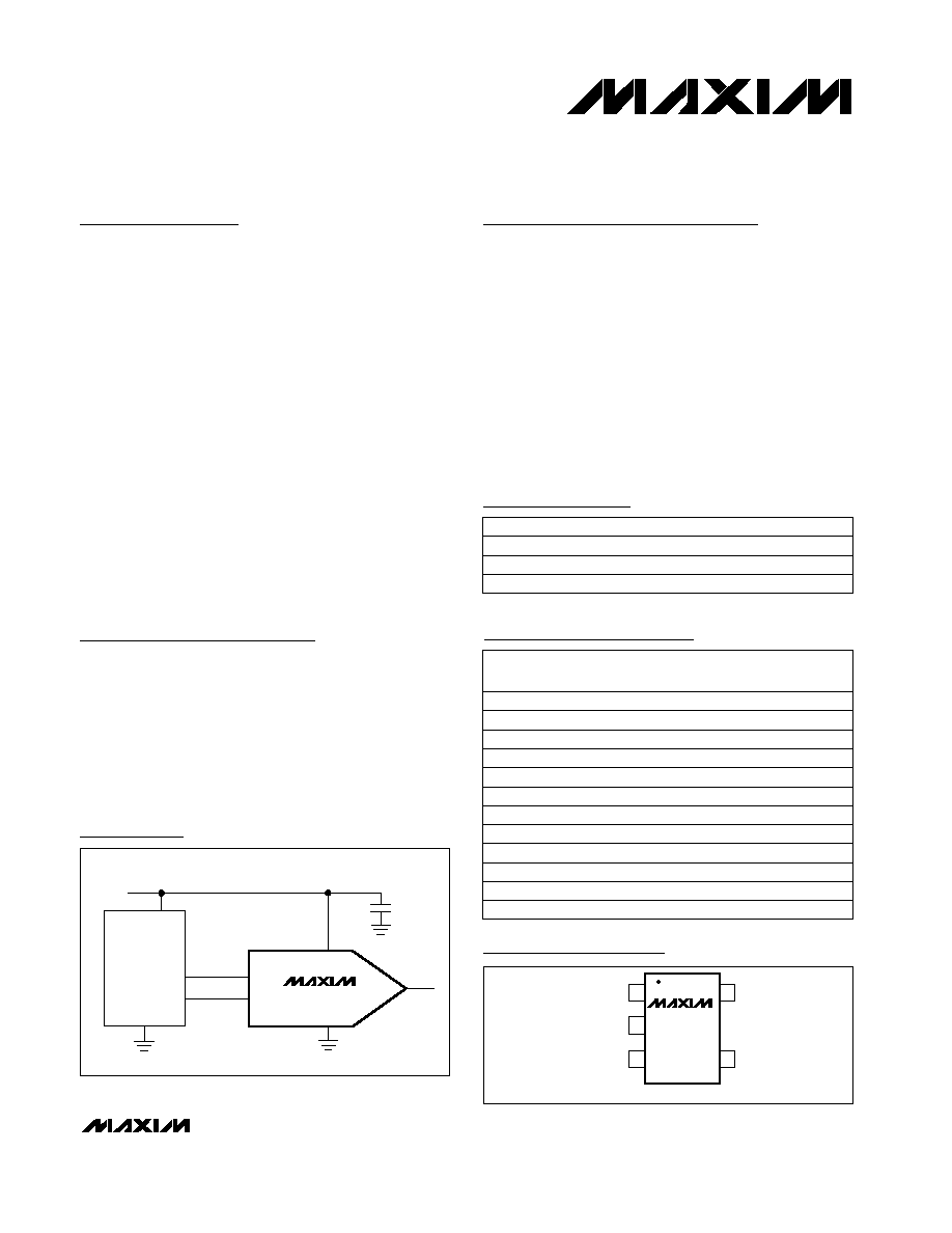
PX.1/SCL
+2.7V TO +5.5V
PX.0/SDA
GND
µC
V
DD
SCL
SDA
OUT
GND
V
DD
MAX5382
Typical Operating Circuit
19-1641; Rev 1; 1/01
Ordering Information
I
2
C is a trademark of Philips Corp.
Selector Guide
PART
MAX5380_EUK-T
MAX5381_EUK-T
MAX5382_EUK-T
-40∞C to +85∞C
-40∞C to +85∞C
-40∞C to +85∞C
TEMP. RANGE
PIN-PACKAGE
5 SOT23
5 SOT23
5 SOT23
PART
MAX5380LEUK
MAX5380MEUK
MAX5380NEUK
0x64
0x62
0x60
ADDRESS
REFERENCE
(V)
+2.0
+2.0
+2.0
MAX5380PEUK
0x66
+2.0
MAX5381LEUK
0x60
+4.0
MAX5381MEUK
0x62
+4.0
MAX5381NEUK
0x64
+4.0
MAX5381PEUK
0x66
+4.0
MAX5382MEUK
0x62
0.9 x V
DD
MAX5382NEUK
0x64
0.9 x V
DD
MAX5382PEUK
0x66
0.9 x V
DD
MAX5382LEUK
0x60
0.9 x V
DD
TOP
MARK
ADMN
ADMZ
ADFN
ADMP
ADMV
ADNB
ADML
ADND
ADNJ
ADNT
ADMX
ADNH
GND
SDA
V
DD
1
5
SCL
OUT
MAX5380
MAX5381
MAX5382
SOT23-5
TOP VIEW
2
3
4
Pin Configuration
________________________________________________________________ Maxim Integrated Products
1
For pricing, delivery, and ordering information, please contact Maxim/Dallas Direct! at
1-888-629-4642, or visit Maxim's website at www.maxim-ic.com.
MAX5380/MAX5381/MAX5382
Low-Cost, Low-Power, 8-Bit DACs with
2-Wire Serial Interface in SOT23
2
_______________________________________________________________________________________
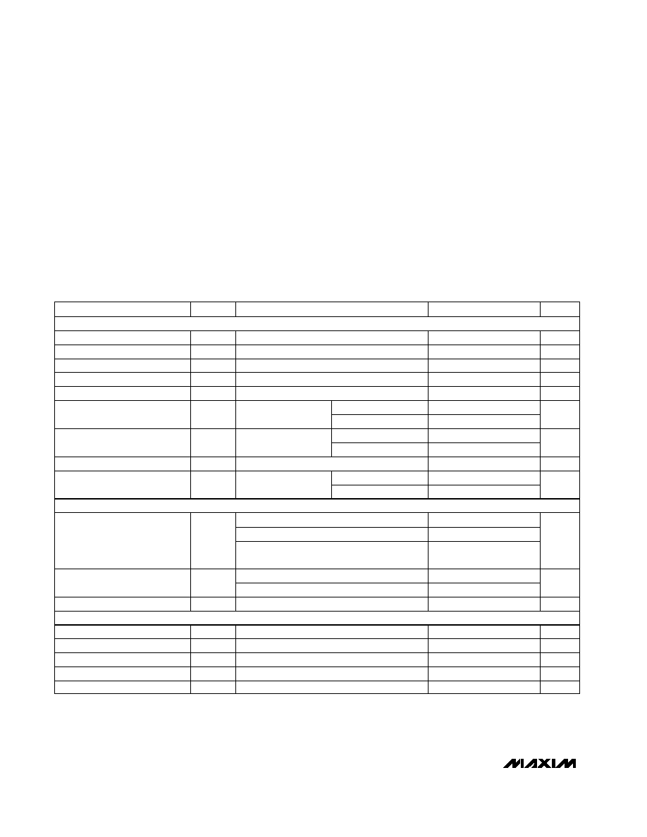
ABSOLUTE MAXIMUM RATINGS
ELECTRICAL CHARACTERISTICS
(V
DD
= +2.7V to +3.6V (MAX5380), V
DD
= +4.5V to +5.5V (MAX5381), V
DD
= +2.7V to +5.5V (MAX5382); R
L
= 10k
; C
L
= 50pF,
T
A
= T
MIN
to T
MAX
, unless otherwise noted. Typical values are T
A
= +25∞C.)
Stresses beyond those listed under "Absolute Maximum Ratings" may cause permanent damage to the device. These are stress ratings only, and functional
operation of the device at these or any other conditions beyond those indicated in the operational sections of the specifications is not implied. Exposure to
absolute maximum rating conditions for extended periods may affect device reliability.
V
DD
to GND ..............................................................-0.3V to +6V
OUT, SCL, SDA to GND ...........................................-0.3V to +6V
Maximum Current into Any Pin............................................50mA
Continuous Power Dissipation (T
A
= +70∞C)
5-Pin SOT23 (derate 7.1mW/∞C above +70∞C).............571mW
Operating Temperature Ranges
MAX538_ _EUK-T .............................................-40∞C to +85∞C
Storage Temperature Range .............................-65∞C to +150∞C
Maximum Junction Temperature .....................................+150∞C
Lead Temperature (soldering, 10s) .................................+300∞C
1.8
2
2.2
MAX5380
MAX5382
MAX5380/MAX5381
MAX5382
MAX5380/MAX5381
MAX5382
MAX5380/MAX5381
Offset Error Temperature
Coefficient
1
ppm/∞C
(Note 2)
Digital-Analog Glitch Impulse
40
nVs
Wake-Up Time
50
µs
Code 127 to 128
From software shutdown
PARAMETER
SYMBOL
MIN
TYP
MAX
UNITS
3
Offset Error Supply Rejection
60
dB
Offset Error
±1
±25
mV
Differential Linearity Error
DNL
±1
LSB
10
Full-Scale Error
5
% of
ideal FS
Full-Scale Error Supply Rejection
50
dB
±40
Resolution
8
Bits
Integral Linearity Error
INL
±1
LSB
Full-Scale Error Temperature
Coefficient
±10
0.85 x
0.9 x
0.95 x
V
DD
V
DD
V
DD
Output Resistance
10
k
Voltage Output Slew Rate
0.4
V/µs
Output Settling Time
20
µs
Digital Feedthrough
2
nVs
CONDITIONS
Code = 255
MAX5382 (Notes 2, 3)
(Note 2)
Guaranteed monotonic
Code = 255
Code = 255, MAX5380/MAX5281 (Note 4)
MAX5382
V
OUT
= 0 to V
DD
, power-down mode
(Note 1)
Positive and negative
To 1/2 LSB, 50k
and 50pF load (Note 6)
Code = 0, all digital inputs from 0 to V
DD
ppm/∞C
0.5
Code = 255, 0 to 100µA
Output Load Regulation
0.5
LSB
Code = 0, 0 to 100µA
V
REF
Internal Reference (Note 5)
MAX5381
3.6
4
4.4
STATIC ACCURACY
DAC OUTPUT
DYNAMIC PERFORMANCE
MAX5380/MAX5381/MAX5382
Low-Cost, Low-Power, 8-Bit DACs with
2-Wire Serial Interface in SOT23
_______________________________________________________________________________________
3
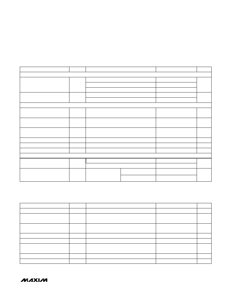
ELECTRICAL CHARACTERISTICS (continued)
(V
DD
= +2.7V to +3.6V (MAX5380), V
DD
= +4.5V to +5.5V (MAX5381), V
DD
= +2.7V to +5.5V (MAX5382); R
L
= 10k
; C
L
= 50pF,
T
A
= T
MIN
to T
MAX
, unless otherwise noted. Typical values are T
A
= +25∞C.)
250
I
SINK
= 6mA
I
SINK
= 3mA
PARAMETER
SYMBOL
MIN
TYP
MAX
UNITS
Supply Current
I
DD
1
150
230
Supply Voltage
V
DD
2.7
5.5
V
Input Low Voltage
V
IL
0.3 x V
DD
V
Input High Voltage
V
IH
0.7 x V
DD
V
Input Hysteresis
V
HYS
0.05 x V
DD
V
Input Capacitance
C
IN
10
pF
2.7
3.6
4.5
5.5
Input Leakage Current
I
IN
±10
µA
Pulse Width of Spike Suppressed
t
SP
0
50
ns
0.4
Output Low Voltage
V
OL
0.6
V
Output Fall Time
t
OF
250
ns
CONDITIONS
Shutdown mode
No load, all digital inputs at 0 or V
DD
, code = 255
MAX5382
I
SINK
= 3mA
(Note 7)
I
SINK
= 6mA
V
IH(MIN)
to V
IL(MAX)
,
bus capacitance =
10pF to 400pF
MAX5380
MAX5381
µA
POWER REQUIREMENTS
DIGITAL INPUTS (SCL, SDA)
DIGITAL OUTPUT (SDA, open drain)
Data Hold Time
t
HD:DAT
0
0.9
µs
Data Setup Time
t
SU:DAT
100
ns
CONDITIONS
µs
0.6
t
SU:STA
Setup Time for a Repeated
START Condition
µs
0.6
t
HIGH
High Period of the SCL Clock
µs
1.3
t
LOW
Low Period of the SCL Clock
kHz
0
400
f
SCL
SCL Clock Frequency
µs
0.6
t
HD:STA
Hold Time Repeated for a
START Condition
µs
1.3
t
BUF
Bus Free Time Between a
STOP and a START Condition
UNITS
MIN
TYP
MAX
SYMBOL
PARAMETER
TIMING CHARACTERISTICS
(Figure 3; V
DD
= +2.7V to +3.6V (MAX5380), V
DD
= +4.5V to +5.5V (MAX5381), V
DD
= +2.7V to +5.5V (MAX5382); R
L
= 10k
;
C
L
= 50pF, T
A
= T
MIN
to T
MAX
, unless otherwise noted. Typical values are T
A
= +25∞C.) (Note 7)
MAX5380/MAX5381/MAX5382
Low-Cost, Low-Power, 8-Bit DACs with
2-Wire Serial Interface in SOT23
4
_______________________________________________________________________________________
TIMING CHARACTERISTICS (continued)
(Figure 3; V
DD
= +2.7V to +3.6V (MAX5380), V
DD
= +4.5V to +5.5V (MAX5381), V
DD
= +2.7V to +5.5V (MAX5382); R
L
= 10k
;
C
L
= 50pF, T
A
= T
MIN
to T
MAX
, unless otherwise noted. Typical values are T
A
= +25∞C.) (Note 7)
Note 1: Guaranteed from code 5 to code 255.
Note 2: The offset value extrapolated from the range over which the INL is guaranteed.
Note 3: MAX5382 tested at V
DD
= +5V ±10%.
Note 4: MAX5380 tested at V
DD
= +3V ±10%, MAX5381 tested at V
DD
= 5V ±10%.
Note 5: Actual output voltages at full scale are 255/256 x V
REF
.
Note 6: Output settling time is measured by taking the code from code 5 to 255, and from code 255 to 5.
Note 7: Guaranteed by design.
Rise Time of Both SDA and
SCL Signals
t
r
300
ns
Fall Time of Both SDA and
SCL Signals
t
f
CONDITIONS
300
ns
Setup Time for STOP Condition
t
SU:STO
0.6
µs
Capacitive Load for Each
Bus Line
C
b
400
pF
UNITS
MIN
TYP
MAX
SYMBOL
PARAMETER
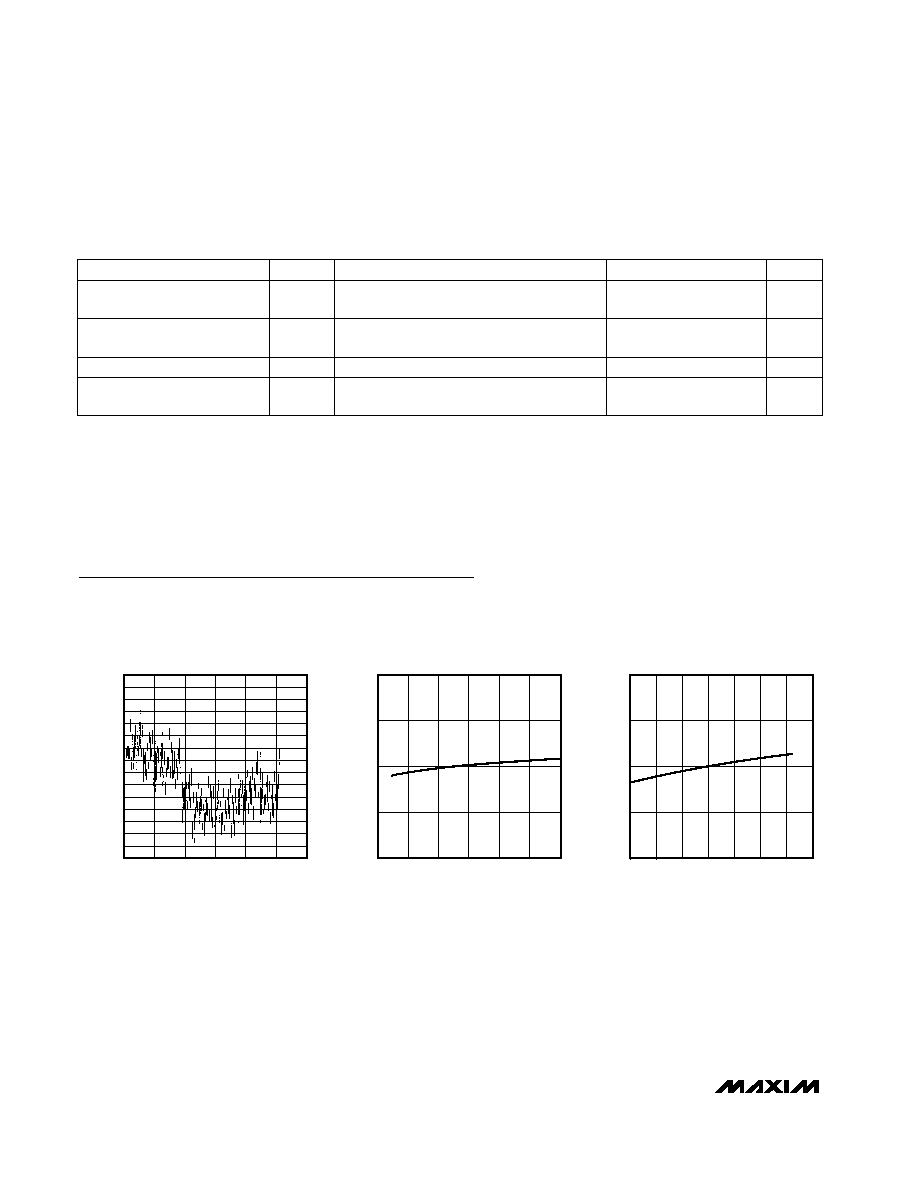
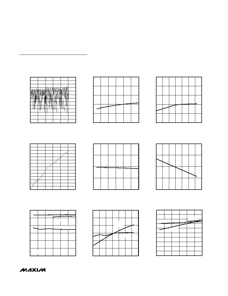
Typical Operating Characteristics
(V
DD
= +3.0V (MAX5380), V
DD
= +5.0V (MAX5381/MAX5382); R
L
= 10k
, T
A
= +25∞C, unless otherwise noted.)
-0.050
-0.075
-0.100
-0.025
0
0.025
0.050
0.075
0
100
200
50
150
250
300
INTEGRAL NONLINEARITY vs. CODE
MAX5380/1/2-01
CODE
INL (LSB)
0
-0.10
-0.15
-0.05
-0.20
2.5
4.0
3.0
3.5
4.5
5.0
5.5
INTEGRAL NONLINEARITY
vs. SUPPLY VOLTAGE
MAX5380/1/2-02
SUPPLY VOLTAGE (V)
INL (LSB)
0
-0.10
-0.15
-0.05
-0.20
-40
20
-20
0
40
60
80
100
INTEGRAL NONLINEARITY
vs. TEMPERATURE
MAX5380/1/2-03
TEMPERATURE (∞C)
INL (LSB)
MAX5380/MAX5381/MAX5382
Low-Cost, Low-Power, 8-Bit DACs with
2-Wire Serial Interface in SOT23
_______________________________________________________________________________________
5
-0.08
-0.04
-0.02
0
0.02
0.04
0
100
200
300
50
150
250
DIFFERENTIAL NONLINEARITY vs. CODE
MAX5380/1/2-04
CODE
DNL (LSB)
-0.06
0
-0.06
-0.08
-0.04
-0.02
-0.10
2.5
4.0
3.0
3.5
4.5
5.0
5.5
DIFFERENTIAL NONLINEARITY
vs. SUPPLY VOLTAGE
MAX5380/1/2-05
SUPPLY VOLTAGE (V)
DNL (LSB)
0
-0.04
-0.06
-0.08
-0.02
-0.10
-40
20
-20
0
40
60
80
100
DIFFERENTIAL NONLINEARITY
vs. TEMPERATURE
MAX5380/1/2-06
TEMPERATURE (∞C)
DNL (LSB)
-0.60
-0.30
-0.45
-0.15
0
0.15
0.30
0.45
0
100
200
300
50
150
250
TOTAL UNADJUSTED ERROR vs. CODE
MAX5380/1/2-07
CODE
TUE (LSB)
0
-1.0
-1.5
-0.5
-2.0
2.5
4.0
3.0
3.5
4.5
5.0
5.5
OFFSET ERROR vs. SUPPLY VOLTAGE
MAX5380/1/2-08
SUPPLY VOLTAGE (V)
V
OS
(mV)
0
-1.0
-0.5
-1.5
-2.0
-40
20
-20
0
40
60
80
100
OFFSET ERROR vs. TEMPERATURE
MAX5380/1/2-09
TEMPERATURE (∞C)
OFFSET ERROR (mV)
Typical Operating Characteristics (continued)
(V
DD
= +3.0V (MAX5380), V
DD
= +5.0V (MAX5381/MAX5382); R
L
= 10k
, T
A
= +25∞C, unless otherwise noted.)
3
1
0
-1
-2
2
-3
2.5
4.0
3.0
3.5
4.5
5.0
5.5
FULL-SCALE ERROR vs. SUPPLY VOLTAGE
MAX5380/1/2-10
SUPPLY VOLTAGE (V)
FULL-SCALE ERROR (LSB)
1.2
0.4
0
-0.4
-0.8
0.8
-1.2
FULL-SCALE ERROR (%)
MAX5381
MAX5380
MAX5382
NO LOAD
3
1
0
-1
-2
2
-3
1.2
0.4
0
-0.4
-0.8
0.8
-1.2
-40
20
-20
0
40
60
80
100
FULL-SCALE ERROR vs. TEMPERATURE
MAX5380/1/2-11
TEMPERATURE (∞C)
FULL-SCALE ERROR (LSB)
FULL-SCALE ERROR (%)
MAX5381
MAX5380
MAX5382
200
140
120
100
60
80
20
40
160
180
0
2.5
4.0
3.0
3.5
4.5
5.0
5.5
SUPPLY CURRENT vs. SUPPLY VOLTAGE
MAX5380/1/2-12
SUPPLY VOLTAGE (V)
SUPPLY CURRENT (
µ
A)
MAX5381
MAX5380
MAX5382