 | ÐлекÑÑоннÑй компоненÑ: MAX5426 | СкаÑаÑÑ:  PDF PDF  ZIP ZIP |
Äîêóìåíòàöèÿ è îïèñàíèÿ www.docs.chipfind.ru
General Description
The MAX5426 is a precision resistor network optimized
for use with programmable instrumentation amplifiers.
The MAX5426 operates from dual ±5V to ±15V supplies
and consumes less than 40µA of supply current.
Designed to be used in the traditional three op amp
instrumentation amplifier topology, this device provides
noninverting gains of 1, 2, 4, and 8 that are accurate to
0.025% (A-grade), 0.09% (B-grade), or 0.5%
(C-grade) over the extended temperature range (-40°C
to +85°C). The MAX5426 is available in the 6.4mm
5mm 14-pin TSSOP package.
Applications
General-Purpose Programmable Instrumentation
Amplifiers
Gain Control in RF Power Amplifiers
Precision Dual Attenuator
Features
o Differential Gains: A
V
= 1, 2, 4, 8
o Gain Accurate to 0.025%, 0.09%, or 0.5%
o Dual Supply ±5V to ±15V Operation
o Low 36µA Supply Current
o Simple CMOS/TTL Logic Compatible 2-Wire
Parallel Interface
o Space-Saving 14-Pin TSSOP Package
(6.4mm
5mm)
o OFFSET Pin Available to Offset the Output of the
Differential Amplifier
MAX5426
Precision Resistor Network for
Programmable Instrumentation Amplifiers
________________________________________________________________ Maxim Integrated Products
1
Ordering Information
19-2318; Rev 0; 1/02
For pricing, delivery, and ordering information, please contact Maxim/Dallas Direct! at
1-888-629-4642, or visit Maxim's website at www.maxim-ic.com.
PART
TEMP
RANGE
PIN-
PACKAGE
GAIN
MAX5426AEUD
-40
°C to +85°C
14 TSSOP
0.025%
MAX5426BEUD
-40
°C to +85°C
14 TSSOP
0.09%
MAX5426CEUD
-40
°C to +85°C
14 TSSOP
0.5%
CM
FB2
INDIF-
OUT2
INDIF+
OUT
OFFSET
V
DD
V
IN-
V
IN+
GND
D1
D0
FB1
OUT1
V
SS
V
OUT
MAX5426
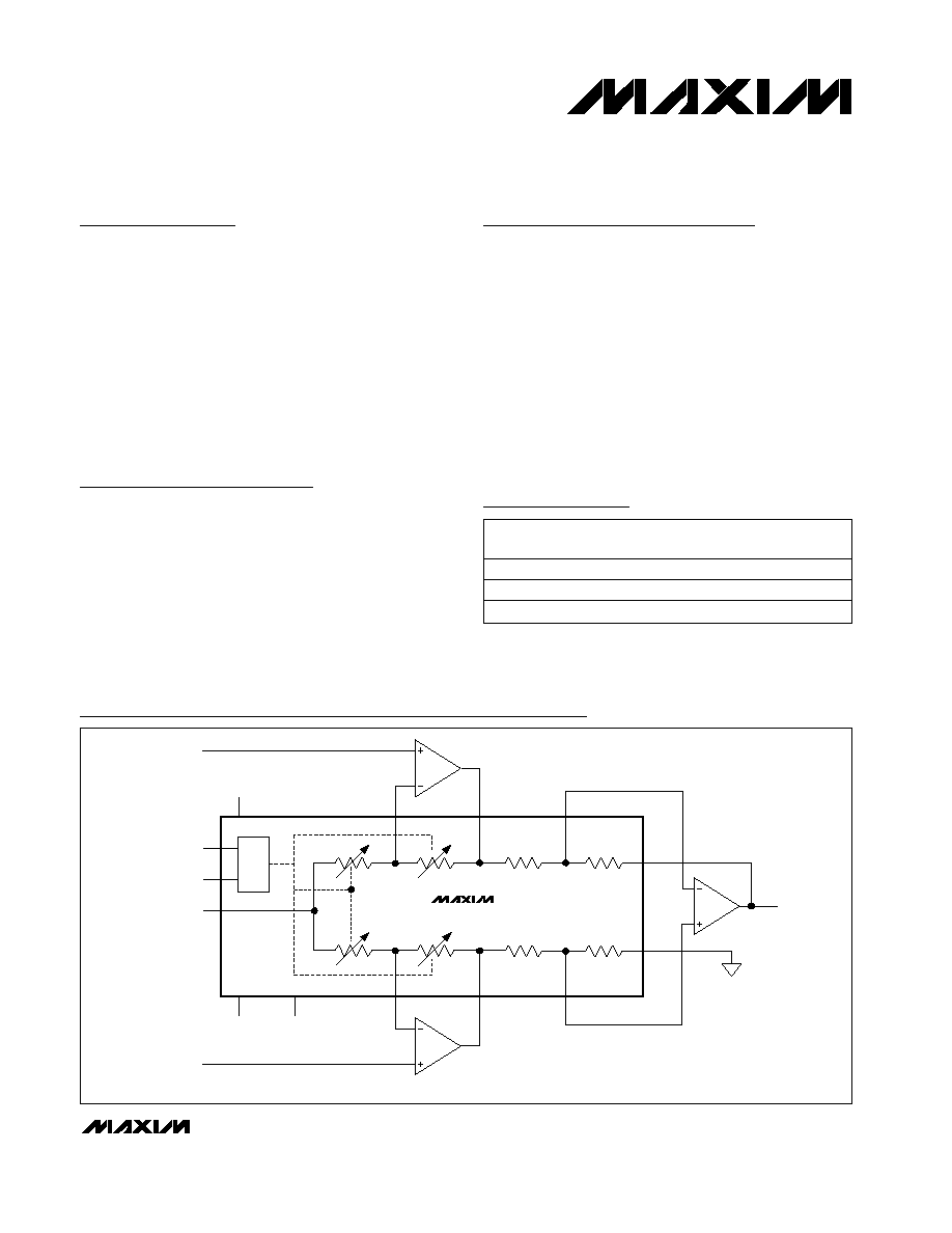
Typical Operating Circuit
Pin Configuration and Functional Diagram appear at
end of data sheet.
MAX5426
Precision Resistor Network for
Programmable Instrumentation Amplifiers
2
_______________________________________________________________________________________
ABSOLUTE MAXIMUM RATINGS
ELECTRICAL CHARACTERISTICS
(V
DD
= +15V, V
SS
= -15V, GND = 0, T
A
= T
MIN
to T
MAX
, unless otherwise noted. Typical values are at T
A
= +25°C.)
Stresses beyond those listed under "Absolute Maximum Ratings" may cause permanent damage to the device. These are stress ratings only, and functional
operation of the device at these or any other conditions beyond those indicated in the operational sections of the specifications is not implied. Exposure to
absolute maximum rating conditions for extended periods may affect device reliability.
V
DD
to GND ............................................................-0.3V to +17V
V
SS
to GND.............................................................-17V to +0.3V
D0, D1 to GND ...........................................-0.3V to (V
DD
+ 0.2V)
D0, D1 to GND (V
DD
> +6V) .................................-0.3V to +6.0V
All Other Pins to GND ......................(V
SS
- 0.3V) to (V
DD
+ 0.2V)
Maximum Current Into V
DD
, V
SS
, D1, D0 .........................±50mA
Maximum Current from OUT1 to CM or OUT2 ..............±0.72mA
Maximum Current from OUT1 to INDIF- or OUT............±0.72mA
Maximum Current from OUT2 to INDIF+ or OFFSET.....±0.72mA
Continuous Power Dissipation (T
A
= +70°C)
14-Pin TSSOP (derate 9.1mW/°C above +70°C) ..........727mW
Operating Temperature Range ...........................-40°C to +85°C
Junction Temperature ......................................................+150°C
Storage Temperature Range .............................-60°C to +150°C
PARAMETER
SYMBOL
CONDITIONS
MIN
TYP
MAX
UNITS
MAX5426A
0.004
0.025
MAX5426B
0.025
0.090
Gain Range Accuracy (Notes 1, 2)
MAX5426C
0.080
0.500
%
Capacitance at Analog Pins
C
ANALOG
5
pF
Gain = 1
79
Gain = 2
85
Gain = 4
91
Differential CMRR (Notes 1, 2)
Gain = 8
97
dB
DIGITAL INPUTS
Input High Voltage
V
IH
2.4
V
Input Low Voltage
V
IL
0.8
V
Input Leakage Current
I
LKG
D1 = D0 = 0 or logic high
10
µA
EQUIVALENT RESISTANCES
Resistance Between OUT1 and
OUT2
R
OUT1,
R
OUT2
56
k
Resistance Between OUT1 and
INDIF-
R
OUT1,
R
INDIF-
26
k
Resistance Between INDIF- and
OUT
R
INDIF-,
R
OUT
26
k
Resistance Between OUT2 and
INDIF+
R
OUT2,
R
INDIF+
26
k
Resistance Between INDIF+ and
OFFSET
R
INDIF+,
R
OFFSET
26
k
Gain = 1
0
Gain = 2
15
Gain = 4
22
Resistance Between OUT1 and
FB1
R
OUT1,
R
FB1
Gain = 8
26
k
MAX5426
Precision Resistor Network for
Programmable Instrumentation Amplifiers
_______________________________________________________________________________________
3
Note 1: Total error when configured as instrumentation amplifier. Assumes ideal op amps.
Note 2: Each stage (input stage and output stage) is tested for accuracy separately and combined to give the total gain accuracy.
The input stage is tested as follows: OUT1 = 10V, OUT2 = 0. Output stage is tested as follows OUT1 = 10V, OUT2 = 0 and
OUT2 = 10V, OFFSET = 0.
Note 3: Gain of 1 configuration is open circuit (infinite impedance).
Note 4: Equivalent load at each pin is calculated according to instrumentation amplifier configuration and assumes ideal op amps.
Note 5: See Timing Diagram.
ELECTRICAL CHARACTERISTICS (continued)
(V
DD
= +15V, V
SS
= -15V, GND = 0, T
A
= T
MIN
to T
MAX
, unless otherwise noted. Typical values are at T
A
= +25°C.)
PARAMETER
SYMBOL
CONDITIONS
MIN
TYP
MAX
UNITS
Gain = 2
29
Gain = 4
15
Resistance Between FB1 and FB2
(Note 3)
R
FB1,
R
FB2
Gain = 8
7
k
Gain = 1
0
Gain = 2
15
Gain = 4
22
Resistance Between OUT2 and
FB2
R
OUT2,
R
FB2
Gain = 8
26
k
Input Impedance at FB1
Z
FB1
0
k
Input Impedance at FB2
Z
FB2
0
k
Gain = 1
0
Gain = 2
9.5
Gain = 4
12
Input Impedance at OUT1
(Note 4)
Z
OUT1
Gain = 8
13
k
Gain = 1
0
Gain = 2
9.5
Gain = 4
12
Input Impedance at OUT2
(Note 4)
Z
OUT2
Gain = 8
13
k
Input Impedance at INDIF+
(Note 4)
Z
INDIF+
0
k
Input Impedance at INDIF-
(Note 4)
Z
INDIF-
0
k
Input Impedance at OUT (Note 4)
Z
OUT
26
k
Input Impedance at OFFSET
(Note 4)
Z
OFFSET
26
k
POWER REQUIREMENTS
Positive Power-Supply Voltage
V
DD
4.75
15.75
V
Negative Power-Supply Voltage
V
SS
-15.75
-4.75
V
D1 = D0 = 0
10
Positive Supply Current
I
DD
D1 = D0 = 5V
36
80
µA
Negative Supply Current
I
SS
0.01
10
µA
TIMING REQUIREMENTS
Switching Time (Note 5)
t
SWITCHING
(Figure 3)
60
ns
MAX5426
Precision Resistor Network for
Programmable Instrumentation Amplifiers
4
_______________________________________________________________________________________
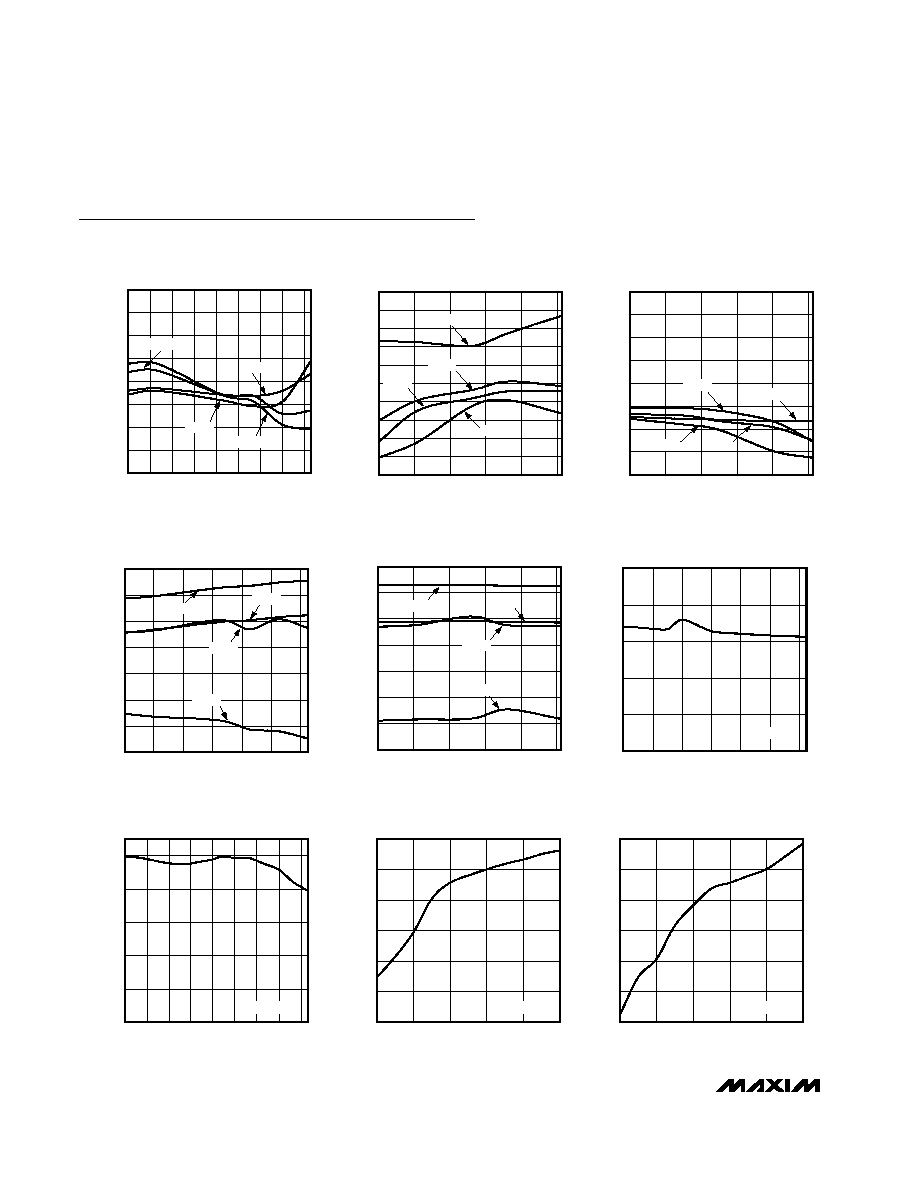
Typical Operating Characteristics
(V
DD
= +15V, V
SS
= -15V, T
A
= +25°C, unless otherwise noted.)
MAX5426A GAIN ACCURACY
vs. TEMPERATURE
MAX5426 toc01
TEMPERATURE (
°C)
GAIN ACCURACY (%)
80
65
-25 -10
5
35
20
50
-0.015
-0.010
-0.005
0
0.005
0.010
0.015
0.020
-0.020
-40
GAIN 4
GAIN 1
GAIN 2
GAIN 8
MAX5426A GAIN ACCURACY
vs. POSITIVE SUPPLY VOLTAGE
MAX5426 toc02
POSITIVE SUPPLY VOLTAGE (V)
GAIN ACCURACY (%)
14.75
12.75
10.75
8.75
6.75
-0.012
-0.010
-0.008
-0.006
-0.004
-0.002
0
0.002
0.004
0.006
-0.014
4.75
GAIN 1
GAIN 4
GAIN 2
GAIN 8
MAX5426A GAIN ACCURACY
vs. NEGATIVE SUPPLY VOLTAGE
MAX5426 toc03
NEGATIVE SUPPLY VOLTAGE (V)
GAIN ACCURACY (%)
-5
-7
-13
-11
-9
-0.015
-0.010
-0.005
0
0.005
0.010
0.015
0.020
-0.020
-15
GAIN 1
GAIN 4
GAIN 8
GAIN 2
MAX5426B GAIN ACCURACY
vs. TEMPERATURE
MAX5426 toc04
TEMPERATURE (
°C)
GAIN ACCURACY (%)
80
60
40
20
0
-20
-0.025
-0.020
-0.015
-0.010
-0.005
0
0.005
-0.030
-40
GAIN 1
GAIN 2
GAIN 4
GAIN 8
MAX5426B GAIN ACCURACY
vs. POSITIVE SUPPLY VOLTAGE
MAX5426 toc05
POSITIVE SUPPLY VOLTAGE (V)
GAIN ACCURACY (%)
14.75
12.75
10.75
8.75
6.75
-0.025
-0.020
-0.015
-0.010
-0.005
0
0.005
-0.030
4.75
GAIN 1
GAIN 4
GAIN 2
GAIN 8
0
3
9
6
12
15
-40
0
-20
20
40
60
80
POSITIVE SUPPLY CURRENT
vs. TEMPERATURE
MAX5426 toc06
TEMPERATURE (
°C)
POSITIVE SUPPLY CURRENT (
µ
A)
D1 = D0 = 0
-10
-8
-6
-4
-2
0
-40
-10
-25
5
20
35
50
65
80
NEGATIVE SUPPLY CURRENT
vs. TEMPERATURE
MAX5426 toc07
TEMPERATURE (
°C)
NEGATIVE SUPPLY CURRENT (
µ
A)
D1 = D0 = 0
5
15
10
25
20
30
35
5
15
POSITIVE SUPPLY CURRENT
vs. POSITIVE SUPPLY VOLTAGE
MAX5426 toc08
POSITIVE SUPPLY VOLTAGE (V)
POSITIVE SUPPLY CURRENT (
µ
A)
9
7
11
13
D1 = D0 = 5V
-1.2
-0.8
-1.0
-0.4
-0.6
-0.2
0
-15
-5
NEGATIVE SUPPLY CURRENT
vs. NEGATIVE SUPPLY VOLTAGE
MAX5426 toc09
NEGATIVE SUPPLY VOLTAGE (V)
NEGATIVE SUPPLY CURRENT (
µ
A)
-11
-13
-9
-7
D1 = D0 = 0
MAX5426
Precision Resistor Network for
Programmable Instrumentation Amplifiers
_______________________________________________________________________________________
5
Detailed Description
The MAX5426 is a precision resistor network with low
temperature drift and high accuracy that performs the
same function as a precision resistor array and CMOS
switches. Operationally, this device consists of fixed
resistors and digitally controlled variable resistors that
provide differential gains of 1, 2, 4, and 8 (see
Functional Diagram). The MAX5426 provides gains
accurate to 0.025% (MAX5426A), 0.09% (MAX5426B)
or 0.5% (MAX5426C).
The MAX5426 is ideal for programmable instrumenta-
tion amplifiers. An offset pin is available to apply a DC
offset voltage to the output of the differential amplifier.
Pin CM is the common-mode input voltage and can be
buffered and connected to the common-mode input of
the instrumentation amplifier (usually the shield of the
input cable to reduce the effects of cable capacitance
and leakage).
Digital Interface Operation
The MAX5426 features a simple two-bit parallel pro-
gramming interface. D1 and D0 program the gain set-
ting according to the Logic-Control Truth Table (see
Table 1). The digital interface is CMOS/TTL logic com-
patible.
Timing Diagram
Figure 3 shows the timing diagram of MAX5426 for two
cases. In case 1, the differential input changes are at
OUT1 and OUT2, while the voltage settling is observed
at FB1 and FB2. The settling time (t
SETTLE
) is defined
as the time for the output voltage (from the change in
the input) to reach (and stay) within 0.02% of its final
value.
In case 2, the differential inputs (OUT1 and OUT2) are
at constant voltages, while D1 and D0 are varied (for
example from 01 to 10) to make a change in the gain.
No op amps are used in these cases.
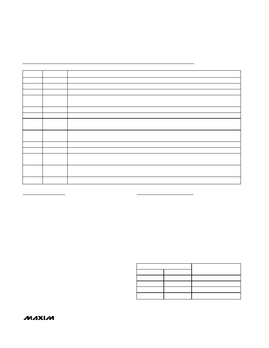
Pin Description
PIN
NAME
FUNCTION
1
V
DD
Positive Power Supply. Bypass V
DD
to GND with a 0.1µF capacitor.
2
GND
Ground
3
V
SS
Negative Power Supply. Bypass V
SS
to GND with a 0.1µF capacitor.
4
FB2
First Stage Positive Input Terminal Resistor. Connect to the inverting terminal of the second input buffer
(see Figure 1).
5
OUT2
First Stage Positive Output Terminal Resistor. Connect to the output terminal of the second input buffer.
6
OFFSET
Second Stage Offset Terminal. Connect to a DC voltage to offset the output of the differential amplifier.
7
INDIF-
Second Stage Negative Input Terminal Resistor. Connect to the inverting input terminal of the
differential op amp.
8
INDIF+
Second Stage Positive Input Terminal Resistor. Connect to the noninverting input terminal of the
differential op amp.
9
OUT
Second Stage Output Terminal, Final Output Terminal
10
OUT1
First Stage Negative Output Terminal of Resistor. Connect to the output terminal of the first input buffer.
11
FB1
First Stage Negative Input Terminal of Resistor. Connect to the inverting input terminal of the first input
buffer.
12
CM
Common-Mode Voltage. CM is the input common-mode voltage of the instrumentation amplifier.
Typically varies ±1% of input common-mode voltage.
13, 14
D0, D1
Digital Inputs. See Table 1.
DIGITAL INPUTS
D1
D0
GAIN
0
0
1
0
1
2
1
0
4
1
1
8
Table 1. Logic-Control Truth Table