 | –≠–ª–µ–∫—Ç—Ä–æ–Ω–Ω—ã–π –∫–æ–º–ø–æ–Ω–µ–Ω—Ç: MAX5512 | –°–∫–∞—á–∞—Ç—å:  PDF PDF  ZIP ZIP |
General Description
The MAX5512≠MAX5515 are dual, 8-bit, ultra-low-
power, voltage-output, digital-to-analog converters
(DACs) offering Rail-to-Rail
Æ
buffered voltage outputs.
The DACs operate from a 1.8V to 5.5V supply and con-
sume less than 5µA, making the devices suitable for
low-power and low-voltage applications. A shutdown
mode reduces overall current, including the reference
input current, to just 0.18µA. The MAX5512≠MAX5515
use a 3-wire serial interface that is compatible with
SPITM, QSPITM, and MICROWIRETM.
Upon power-up, the MAX5512≠MAX5515 outputs are
driven to zero scale, providing additional safety for
applications that drive valves or for other transducers
that need to be off during power-up. The zero-scale
outputs enable glitch-free power-up.
The MAX5512 accepts an external reference input and
provides unity-gain outputs. The MAX5513 contains a
precision internal reference and provides a buffered
external reference output with unity-gain DAC outputs.
The MAX5514 accepts an external reference input and
provides force-sense outputs. The MAX5515 contains a
precision internal reference and provides a buffered
external reference output with force-sense DAC outputs.
The MAX5514/MAX5515 are available in a 4mm x 4mm
x 0.8mm, 12-pin, thin QFN package. The MAX5512/
MAX5513 are available in an 8-pin µMAX package. All
devices are guaranteed over the extended -40∞C to
+85∞C temperature range.
For 10-bit compatible devices, refer to the MAX5522≠
MAX5525 data sheet. For 12-bit compatible devices,
refer to the MAX5532≠MAX5535 data sheet.
Applications
Portable Battery-Powered Devices
Instrumentation
Automatic Trimming and Calibration in Factory
or Field
Programmable Voltage and Current Sources
Industrial Process Control and Remote
Industrial Devices
Remote Data Conversion and Monitoring
Chemical Sensor Cell Bias for Gas Monitors
Programmable LCD Bias
Features
Ultra-Low 5µA Supply Current
Shutdown Mode Reduces Supply Current to
0.18µA (max)
Single +1.8V to +5.5V Supply
Small 4mm x 4mm x 0.8mm Thin QFN Package
Internal Reference Sources 8mA of Current
(MAX5513/MAX5515)
Flexible Force-Sense-Configured Rail-to-Rail
Output Buffers
Fast 16MHz, 3-Wire, SPI-/QSPI-/MICROWIRE-
Compatible Serial Interface
TTL- and CMOS-Compatible Digital Inputs with
Hysteresis
Glitch-Free Outputs During Power-Up
MAX5512≠MAX5515
Dual, Ultra-Low-Power,
8-Bit, Voltage-Output DACs
________________________________________________________________ Maxim Integrated Products
1
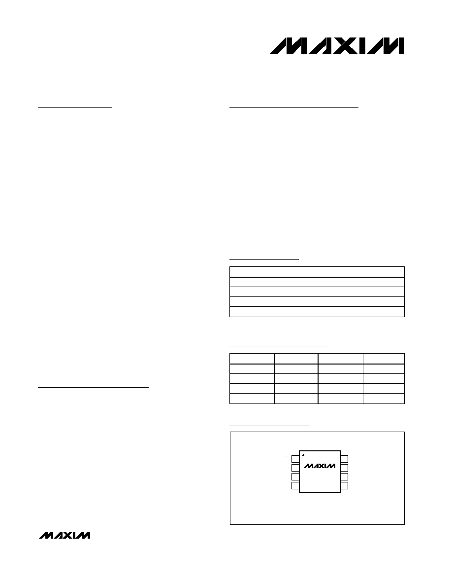
Ordering Information
19-3066; Rev 0; 1/04
For pricing, delivery, and ordering information, please contact Maxim/Dallas Direct! at
1-888-629-4642, or visit Maxim's website at www.maxim-ic.com.
* EP = Exposed paddle (internally connected to GND).
Pin Configurations continued at end of data sheet.
PART
TEMP RANGE
PIN-PACKAGE
MAX5512
EUA
-40∞C to +85∞C
8 µMAX
MAX5513
EUA
-40∞C to +85∞C
8 µMAX
MAX5514
ETC
-40∞C to +85∞C
12 Thin QFN-EP*
MAX5515
ETC
-40∞C to +85∞C
12 Thin QFN-EP*
Rail-to-Rail is a registered trademark of Nippon Motorola, Inc.
SPI and QSPI are trademarks of Motorola, Inc.
MICROWIRE is a trademark of National Semiconductor Corp.
Selector Guide
PART
OUTPUTS
REFERENCE
TOP MARK
MAX5512EUA
Unity gain
External
--
MAX5513EUA
Unity gain
Internal
--
MAX5514ETC
Force sense
External
AACI
MAX5515ETC
Force sense
Internal
AACJ
1
2
3
4
8
7
6
5
OUTA
GND
V
DD
OUTB
REFIN(MAX5512)
REFOUT(MAX5513)
DIN
SCLK
CS
MAX5512
MAX5513
µ
MAX
TOP VIEW
Pin Configurations
MAX5512≠MAX5515
Dual, Ultra-Low-Power,
8-Bit, Voltage-Output DACs
2
_______________________________________________________________________________________
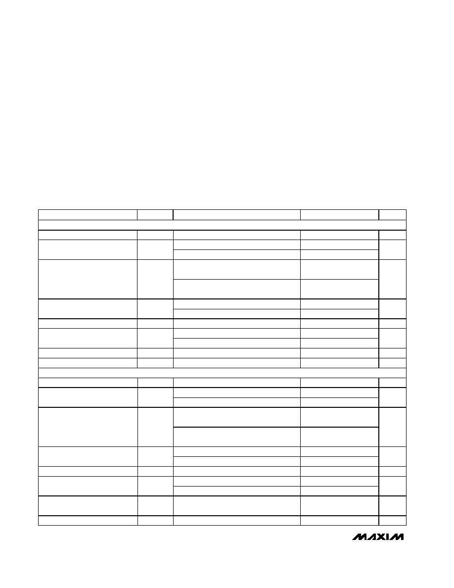
ABSOLUTE MAXIMUM RATINGS
ELECTRICAL CHARACTERISTICS
(V
DD
= +1.8V to +5.5V, OUT_ unloaded, T
A
= T
MIN
to T
MAX
, unless otherwise noted. Typical values are at T
A
= +25∞C.)
Stresses beyond those listed under "Absolute Maximum Ratings" may cause permanent damage to the device. These are stress ratings only, and functional
operation of the device at these or any other conditions beyond those indicated in the operational sections of the specifications is not implied. Exposure to
absolute maximum rating conditions for extended periods may affect device reliability.
V
DD
to GND ..............................................................-0.3V to +6V
OUTA, OUTB to GND .................................-0.3V to (V
DD
+ 0.3V)
FBA, FBB to GND .......................................-0.3V to (V
DD
+ 0.3V)
SCLK, DIN, CS to GND ..............................-0.3V to (V
DD
+ 0.3V)
REFIN, REFOUT to GND ............................-0.3V to (V
DD
+ 0.3V)
Continuous Power Dissipation (T
A
= +70∞C)
12-Pin Thin QFN (derate 16.9mW/∞C above +70∞C).....1349mW
8-Pin µMAX (derate 5.9mW/∞C above +70∞C) .............471mW
Operating Temperature Range ...........................-40∞C to +85∞C
Storage Temperature Range .............................-65∞C to +150∞C
Junction Temperature ......................................................+150∞C
Lead Temperature (soldering, 10s) .................................+300∞C
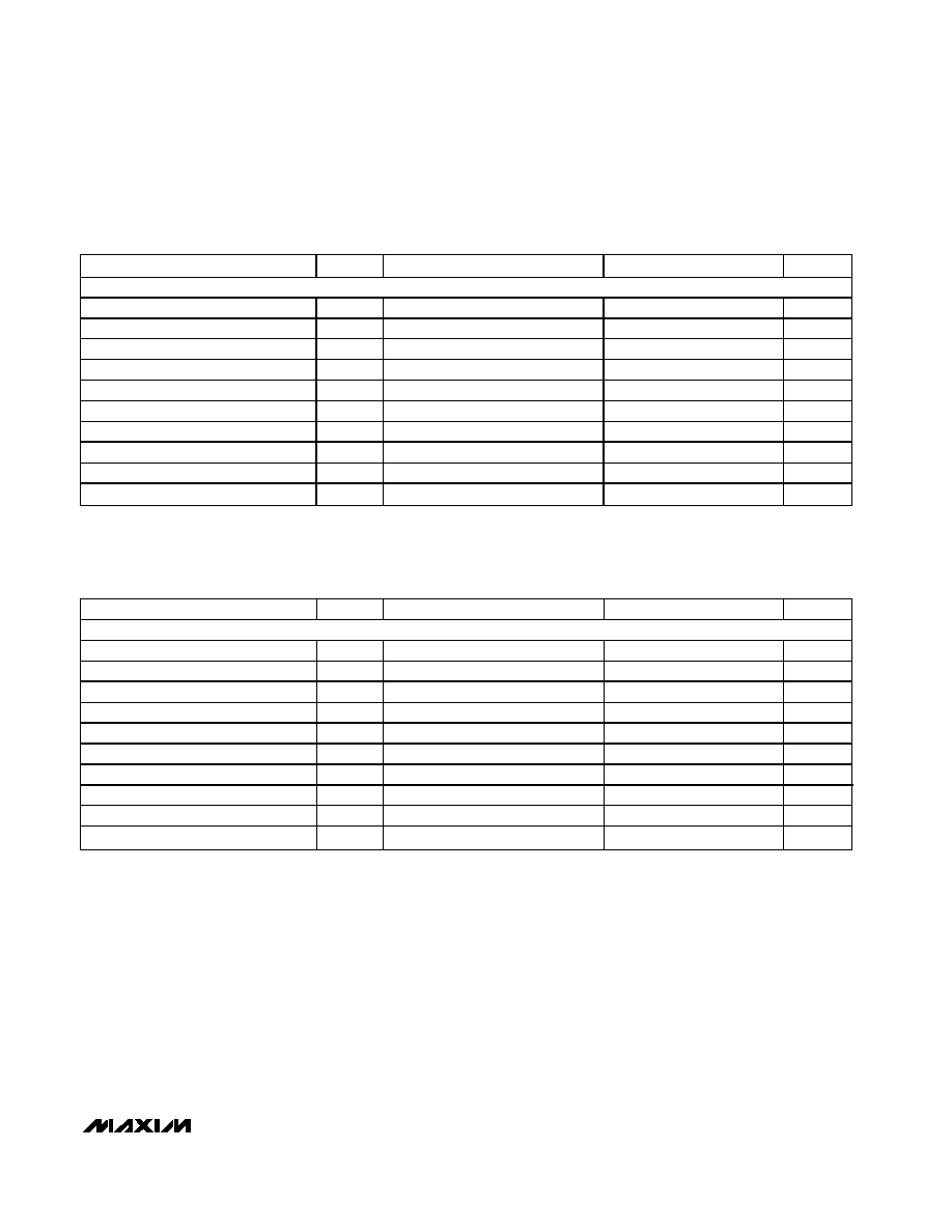
PARAMETER
SYMBOL
CONDITIONS
MIN
TYP
MAX
UNITS
STATIC ACCURACY (MAX5512/MAX5514 EXTERNAL REFERENCE)
Resolution
N
8
Bits
V
DD
= 5V, V
REF
= 4.096V
±0.25
±1
Integral Nonlinearity (Note 1)
INL
V
DD
= 1.8V, V
REF
= 1.024V
±0.25
±1
LSB
Guaranteed monotonic, V
DD
= 5V,
V
REF
= 4.096V
±0.2
±1
Differential Nonlinearity (Note 1)
DNL
Guaranteed monotonic, V
DD
= 1.8V,
V
REF
= 1.024V
±0.2
±1
LSB
V
DD
= 5V, V
REF
= 4.096V
±1
±20
Offset Error (Note 2)
V
OS
V
DD
= 1.8V, V
REF
= 1.024V
±1
±20
mV
Offset-Error Temperature Drift
±2
µV/∞C
V
DD
= 5V, V
REF
= 4.096V
±0.5
±1
Gain Error (Note 3)
GE
V
DD
= 1.8V, V
REF
= 1.024V
±0.5
±1
LSB
Gain-Error Temperature
±4
ppm/∞C
Power-Supply Rejection Ratio
PSRR
1.8V
V
DD
5.5V
85
dB
STATIC ACCURACY (MAX5513/MAX5515 INTERNAL REFERENCE)
Resolution
N
8
Bits
V
DD
= 5V, V
REF
= 3.9V
±0.25
±1
Integral Nonlinearity (Note 1)
INL
V
DD
= 1.8V, V
REF
= 1.2V
±0.25
±1
LSB
Guaranteed monotonic, V
DD
= 5V,
V
REF
= 3.9V
±0.2
±1
Differential Nonlinearity (Note 1)
DNL
Guaranteed monotonic, V
DD
= 1.8V,
V
REF
= 1.2V
±0.2
±1
LSB
V
DD
= 5V, V
REF
= 3.9V
±1
±20
Offset Error (Note 2)
V
OS
V
DD
= 1.8V, V
REF
= 1.2V
±1
±20
mV
Offset-Error Temperature Drift
±2
µV/∞C
V
DD
= 5V, V
REF
= 3.9V
±0.5
±1
Gain Error (Note 3)
GE
V
DD
= 1.8V, V
REF
= 1.2V
±0.5
±1
LSB
Gain-Error Temperature
Coefficient
±4
ppm/∞C
Power-Supply Rejection Ratio
PSRR
1.8V
V
DD
5.5V
85
dB
MAX5512≠MAX5515
Dual, Ultra-Low-Power,
8-Bit, Voltage-Output DACs
_______________________________________________________________________________________
3
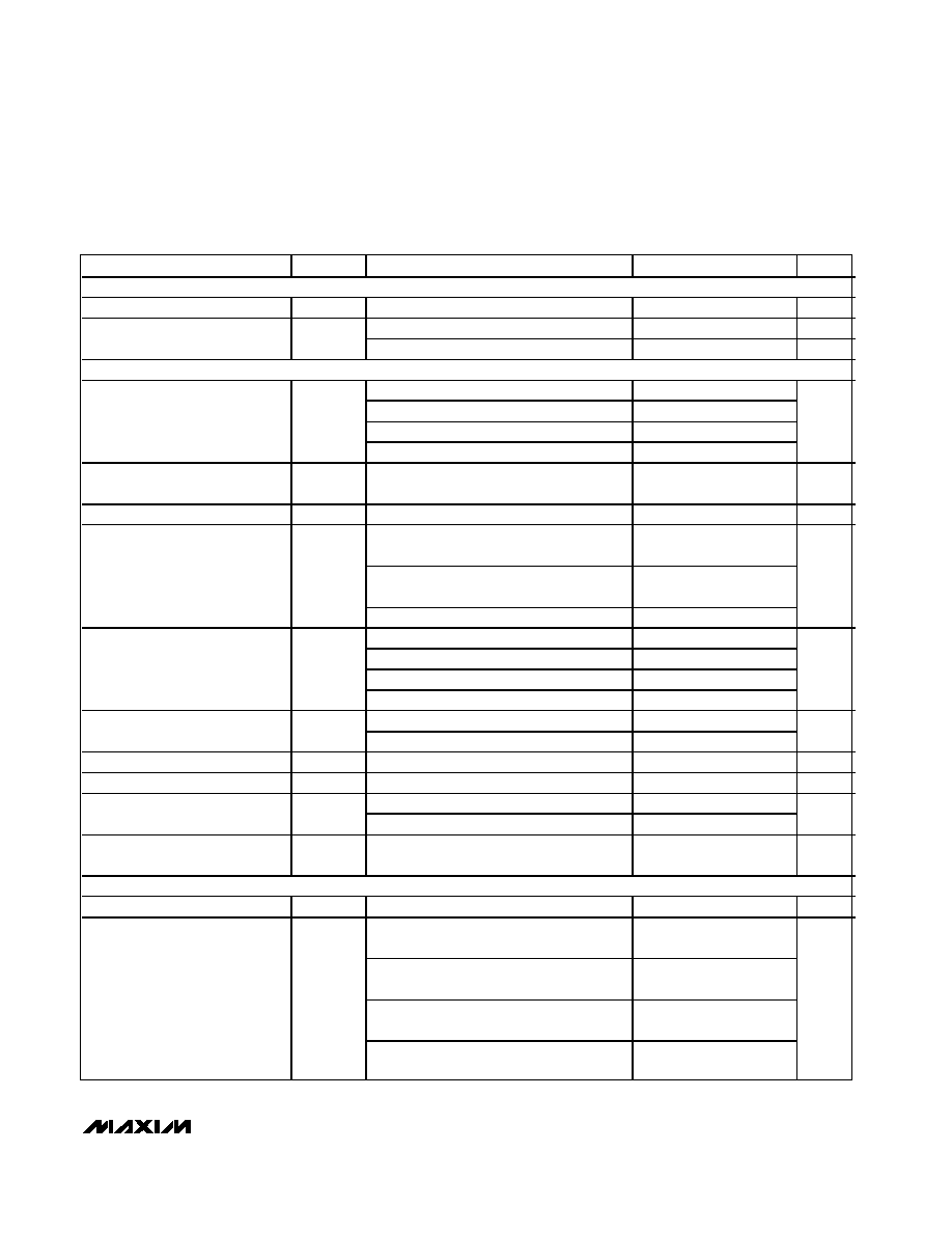
ELECTRICAL CHARACTERISTICS (continued)
(V
DD
= +1.8V to +5.5V, OUT_ unloaded, T
A
= T
MIN
to T
MAX
, unless otherwise noted. Typical values are at T
A
= +25∞C.)
PARAMETER
SYMBOL
CONDITIONS
MIN
TYP
MAX
UNITS
REFERENCE INPUT (MAX5512/MAX5514)
Reference-Input Voltage Range
V
REFIN
0
V
DD
V
Normal operation
4.1
M
Reference-Input Impedance
R
REFIN
In shutdown
2.5
G
REFERENCE OUTPUT (MAX5513/MAX5515)
No external load, V
DD
= 1.8V
1.197
1.214
1.231
No external load, V
DD
= 2.5V
1.913
1.940
1.967
No external load, V
DD
= 3V
2.391
2.425
2.459
Initial Accuracy
V
REFOUT
No external load, V
DD
= 5V
3.828
3.885
3.941
V
Output-Voltage Temperature
Coefficient (Note 4)
V
TEMPCO
T
A
= -40∞C to +85∞C
12
30
ppm/∞C
Line Regulation
V
REFOUT
< V
DD
- 200mV (Note 5)
12
200
µV/V
0
I
REFOUT
1mA, sourcing, V
DD
= 1.8V,
V
REF
= 1.2V
0.3
2
0
I
REFOUT
8mA, sourcing, V
DD
= 5V,
V
REF
= 3.9V
0.3
2
Load Regulation
-150µA
I
REFOUT
0, sinking
0.2
µV/µA
0.1Hz to 10Hz, V
REF
= 3.9V
150
10Hz to 10kHz, V
REF
= 3.9V
600
0.1Hz to 10Hz, V
REF
= 1.2V
50
Output Noise Voltage
10Hz to 10kHz, V
REF
= 1.2V
450
µV
P-P
V
DD
= 5V
30
Short-Circuit Current (Note 6)
V
DD
= 1.8V
14
mA
C ap aci ti ve Load S tab i l i ty Rang e
( N ote 7)
0 to 10
nF
Thermal Hysteresis
(Note 8)
200
ppm
REFOUT unloaded, V
DD
= 5V
5.4
Reference Power-Up Time
(from Shutdown)
REFOUT unloaded, V
DD
= 1.8V
4.4
ms
Long-Term Stability
200
ppm/
1khrs
DAC OUTPUTS (OUTA, OUTB)
Capacitive Driving Capability
C
L
1000
pF
V
DD
= 5V, V
OUT
set to full scale, OUT
shorted to GND, source current
65
V
DD
= 5V, V
OUT
set to 0V,
OUT shorted to V
DD
, sink current
65
V
D D
= 1.8V , V
OU T
set to ful l scal e, OU T
shor ted to G N D , sour ce cur r ent
14
Short-Circuit Current (Note 6)
V
DD
= 1.8V, VOUT set to 0V,
OUT shorted to V
DD
, sink current
14
mA
MAX5512≠MAX5515
Dual, Ultra-Low-Power,
8-Bit, Voltage-Output DACs
4
_______________________________________________________________________________________
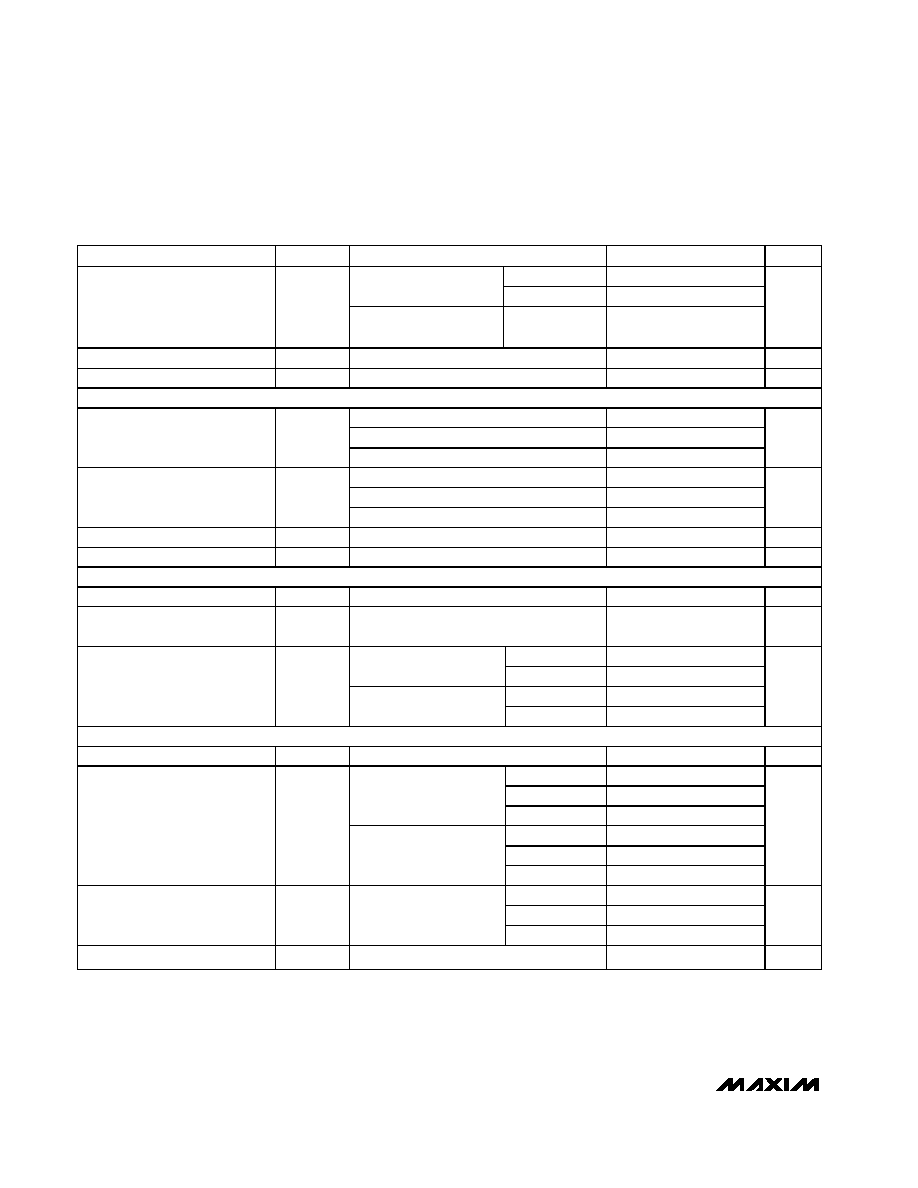
ELECTRICAL CHARACTERISTICS (continued)
(V
DD
= +1.8V to +5.5V, OUT_ unloaded, T
A
= T
MIN
to T
MAX
, unless otherwise noted. Typical values are at T
A
= +25∞C.)
PARAMETER
SYMBOL
CONDITIONS
MIN
TYP
MAX
UNITS
V
DD
= 5V
3
C omi ng out of shutdow n
(MAX5512/MAX5514)
V
DD
= 1.8V
3.8
DAC Power-Up Time
C omi ng out of standb y
(MAX5513/MAX5515)
V
DD
= 1.8V to
V
DD
= 5V
0.4
ms
Output Power-Up Glitch
C
L
= 100pF
10
mV
FB_ Input Current
10
pA
DIGITAL INPUTS (SCLK, DIN,
CS
)
4.5V
V
DD
5.5V
2.4
2.7V
<
V
DD
3.6V
2.0
Input High Voltage
V
IH
1.8V
V
DD
2.7V
0.7 x V
DD
V
4.5V
V
DD
5.5V
0.8
2.7V
<
V
DD
3.6V
0.6
Input Low Voltage
V
IL
1.8V
V
DD
2.7V
0.3 x V
DD
V
Input Leakage Current
I
IN
(Note 9)
±0.05
±0.5
µA
Input Capacitance
C
IN
10
pF
DYNAMIC PERFORMANCE
Voltage-Output Slew Rate
SR
Positive and negative (Note 10)
10
V/ms
Voltage-Output Settling Time
0.1 to 0.9 of full scale to within 0.5 LSB
(Note 10)
660
µs
V
DD
= 5V
80
0.1Hz to 10Hz
V
DD
= 1.8V
55
V
DD
= 5V
620
Output Noise Voltage
10Hz to 10kHz
V
DD
= 1.8V
476
µV
P-P
POWER REQUIREMENTS
Supply Voltage Range
V
DD
1.8
5.5
V
V
DD
= 5V
7.0
8.0
V
DD
= 3V
6.4
8.0
MAX5513/MAX5515
V
DD
= 1.8V
7.0
8.0
V
DD
= 5V
3.8
5.0
V
DD
= 3V
3.8
5.0
Supply Current (Note 9)
I
DD
MAX5512/MAX5514
V
DD
= 1.8V
4.7
6.0
µA
V
DD
= 5V
3.3
4.5
V
DD
= 3V
2.8
4.0
Standby Supply Current
I
DDSD
MAX5513/MAX5515
(Note 9)
V
DD
= 1.8V
2.4
3.5
µA
Shutdown Supply Current
I
DDPD
(Note 9)
0.05
0.25
µA
MAX5512≠MAX5515
Dual, Ultra-Low-Power,
8-Bit, Voltage-Output DACs
_______________________________________________________________________________________
5
Note 1:
Linearity is tested within codes 6 to 255.
Note 2:
Offset is tested at code 6.
Note 3:
Gain is tested at code 255. For the MAX5514/MAX5515, FB_ is connected to its respective OUT_.
Note 4:
Guaranteed by design. Not production tested.
Note 5:
V
DD
must be a minimum of 1.8V.
Note 6:
Outputs can be shorted to V
DD
or GND indefinitely, provided that package power dissipation is not exceeded.
Note 7:
Optimal noise performance is at 2nF load capacitance.
Note 8:
Thermal hysteresis is defined as the change in the initial +25∞C output voltage after cycling the device from T
MAX
to T
MIN
.
Note 9:
All digital inputs at V
DD
or GND.
Note 10:
Load = 10k in parallel with 100pF, V
DD
= 5V, VREF = 4.096V (MAX5512/MAX5514) or V
REF
= 3.9V (MAX5513/MAX5515).
TIMING CHARACTERISTICS
(V
DD
= +4.5V to +5.5V, T
A
= T
MIN
to T
MAX
, unless otherwise noted. Typical values are at T
A
= +25∞C.)
PARAMETER
SYMBOL
CONDITIONS
MIN
TYP
MAX
UNITS
TIMING CHARACTERISTICS (V
DD
= 4.5V to 5.5V )
Serial Clock Frequency
f
SCLK
0
16.7
MHz
DIN to SCLK Rise Setup Time
t
DS
15
ns
DIN to SCLK Rise Hold Time
t
DH
0
ns
SCLK Pulse-Width High
t
CH
24
ns
SCLK Pulse-Width Low
t
CL
24
ns
CS Pulse-Width High
t
CSW
100
ns
SCLK Rise to
CS Rise Hold Time
t
CSH
0
ns
CS Fall to SCLK Rise Setup Time
t
CSS
20
ns
SCLK Fall to
CS Fall Setup
t
CSO
0
ns
CS Rise to SCK Rise Hold Time
t
CS1
20
ns
TIMING CHARACTERISTICS
(VDD = +1.8V to +5.5V, TA = TMIN to TMAX, unless otherwise noted. Typical values are at TA = +25∞C.)
PARAMETER
SYMBOL
CONDITIONS
MIN
TYP
MAX
UNITS
TIMING CHARACTERISTICS (V
DD
= 1.8V to 5.5V )
Serial Clock Frequency
f
SCLK
0
10
MHz
DIN to SCLK Rise Setup Time
t
DS
24
ns
DIN to SCLK Rise Hold Time
t
DH
0
ns
SCLK Pulse-Width High
t
CH
40
ns
SCLK Pulse-Width Low
t
CL
40
ns
CS Pulse-Width High
t
CSW
150
ns
SCLK Rise to
CS Rise Hold Time
t
CSH
0
ns
CS Fall to SCLK Rise Setup Time
t
CSS
30
ns
SCLK Fall to
CS Fall Setup
t
CSO
0
ns
CS Rise to SCK Rise Hold Time
t
CS1
30
ns