 | –≠–ª–µ–∫—Ç—Ä–æ–Ω–Ω—ã–π –∫–æ–º–ø–æ–Ω–µ–Ω—Ç: MAX552 | –°–∫–∞—á–∞—Ç—å:  PDF PDF  ZIP ZIP |
For free samples & the latest literature: http://www.maxim-ic.com, or phone 1-800-998-8800.
For small orders, phone 408-737-7600 ext. 3468.
_______________General Description
The MAX551/MAX552 are 12-bit, current-output, 4-quad-
rant multiplying digital-to-analog converters (DACs).
These devices are capable of providing unipolar or
bipolar outputs when operating from either a single +5V
(MAX551) or +3V (MAX552) power supply. An internal
power-on-reset circuit clears all DAC registers on
power-up, setting the DAC output voltage to 0V.
The SPITM/QSPITM and MicrowireTM-compatible 3-wire
serial interface saves board space and reduces power
dissipation compared with parallel-interface devices.
The MAX551/MAX552 feature double-buffered interface
logic with a 12-bit input register and a 12-bit DAC regis-
ter. Data in the DAC register sets the DAC output volt-
age. Data is loaded into the input register via the serial
interface. The LOAD input transfers data from the input
register to the DAC register, updating the DAC output
voltage.
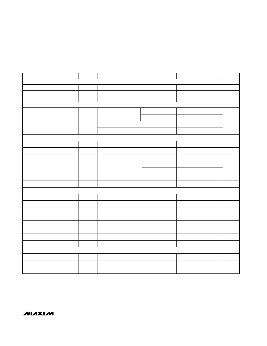
The MAX551/MAX552 are available in an 8-pin DIP
package or a space-saving 10-pin µMAX package. The
µMAX package provides an asynchronous clear (CLR)
input that clears all DAC registers when pulled to GND,
setting the output voltage to 0V.
________________________Applications
Automatic Calibration
Gain Adjustment
Transducer Drivers
Process-Control I/O Boards
Digitally Controlled Filters
Motion-Controlled Systems
µP-Controlled Systems
Programmable Amplifiers/Attenuators
____________________________Features
o
Single-Supply Operation:
+4.5V to +5.25V (MAX551)
+2.7V to +3.6V (MAX552)
o
12.5MHz 3-Wire Serial Interface
o
SPI/QSPI and Microwire Compatible
o
Power-On Reset Clears DAC Output to Zero
o
Asynchronous Clear Input Clears DAC Output
to Zero
o
Voltage Mode or Bipolar Mode Operation with
a Single Power Supply
o
Schmitt-Trigger Digital Inputs for Direct
Optocoupler Interface
o
0.4µA Supply Current
o
10-Pin µMAX Package
MAX551/MAX552
+3V/+5V, 12-Bit, Serial, Multiplying DACs
in 10-Pin µMAX Package
________________________________________________________________
Maxim Integrated Products
1
1
2
3
4
5
10
9
8
7
6
RFB
REF
CLR
SCLK
V
DD
GND
AGND
OUT
MAX551
MAX552
µ
MAX
TOP VIEW
DIN
LOAD
SCLK
DIN
LOAD
1
2
8
7
RFB
REF
GND
V
DD
OUT
DIP
3
4
6
5
MAX551
MAX552
19-1260; Rev 0; 10/97
PART
MAX551
ACPA
MAX551BCPA
MAX551ACUB
0∞C to +70∞C
0∞C to +70∞C
0∞C to +70∞C
TEMP. RANGE
PIN-
PACKAGE
8 Plastic DIP
8 Plastic DIP
10 µMAX
______________Ordering Information
Ordering Information continued at end of data sheet.
SPI and QSPI are trademarks of Motorola Inc. Microwire is a trademark of National Semiconductor Corp.
MAX551BCUB
MAX551AEPA
MAX551BEPA
-40∞C to +85∞C
-40∞C to +85∞C
0∞C to +70∞C
10 µMAX
8 Plastic DIP
8 Plastic DIP
MAX551AEUB
-40∞C to +85∞C
10 µMAX
MAX551BEUB
-40∞C to +85∞C
10 µMAX
LINEARITY
(LSB)
±1/2
±1
±1/2
±1
±1/2
±1
±1/2
±1
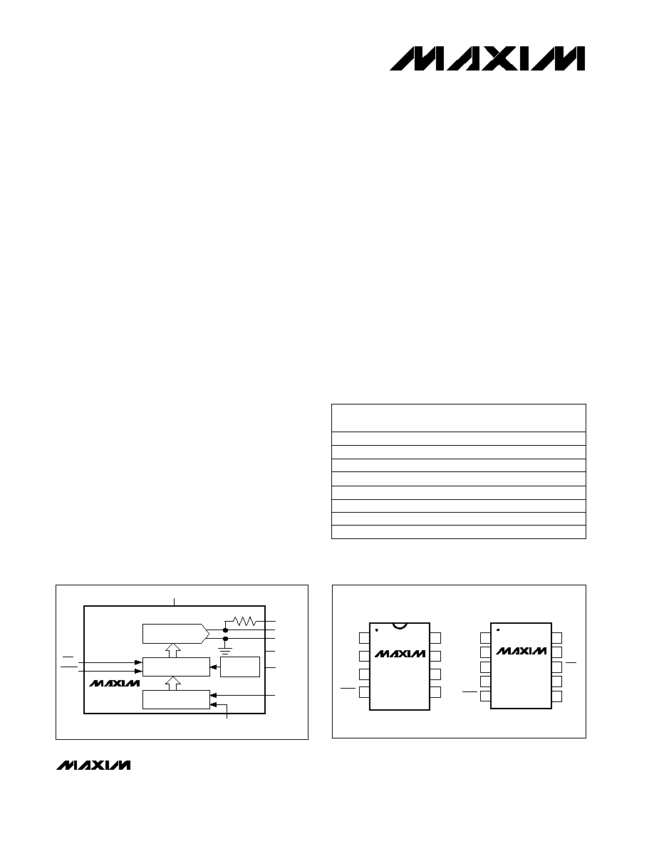
_________________Pin Configurations
12-BIT
D/A CONVERTER
RFB
OUT
AGND*
CLR*
LOAD
V
DD
REF
SCLK
GND
*
µ
MAX PACKAGE ONLY
12-BIT
DAC REGISTER
DIN
R
FB
12-BIT
SHIFT REGISTER
POWER-ON
RESET
MAX551
MAX552
________________Functional Diagram

MAX551/MAX552
+3V/+5V, 12-Bit, Serial, Multiplying DACs
in 10-Pin µMAX Package
2
_______________________________________________________________________________________
ABSOLUTE MAXIMUM RATINGS
ELECTRICAL CHARACTERISTICS--MAX551
(V
DD
= +4.5V to +5.25V, V
REF
= 5V, OUT = AGND = GND, T
A
= T
MIN
to T
MAX
, unless otherwise noted. Typical values are at
T
A
= +25∞C.) (Note 1)
Stresses beyond those listed under "Absolute Maximum Ratings" may cause permanent damage to the device. These are stress ratings only, and functional
operation of the device at these or any other conditions beyond those indicated in the operational sections of the specifications is not implied. Exposure to
absolute maximum rating conditions for extended periods may affect device reliability.
V
DD
to GND..............................................................................6V
REF, RFB to GND.................................................................±12V
Digital Inputs (SCLK, DIN, LOAD, CLR)
to GND .....................................................................-0.3V to 6V
OUT to GND ...............................................-0.3V to (V
DD
+ 0.3V)
AGND to GND ............................................-0.3V to (V
DD
+ 0.3V)
Continuous Power Dissipation (T
A
= +70∞C)
Plastic DIP (derate 9.09mW/∞C above +70∞C) .............727mW
µMAX (derate 5.60mW/∞C above +70∞C) .....................444mW
Operating Temperature Ranges
MAX55_ _C_ _......................................................0∞C to +70∞C
MAX55_ _E_ _ ...................................................-40∞C to +85∞C
Storage Temperature Range .............................-65∞C to +150∞C
Lead Temperature (soldering, 10sec) .............................+300∞C
V
REF
= 6V
RMS
at 1kHz, DAC register loaded
with all 1s
V
REF
= 5Vp-p at 10kHz, DAC register loaded
with all 0s
Using internal feedback resistor (R
FB
)
(Note 2)
V
DD
= +5%, -10%
T
A
= +25∞C, to 1/2LSB, OUT load is
100
||13pF, DAC register alternately loaded
with 1s and 0s
10Hz to 100kHz, measured between RFB and
OUT
CONDITIONS
nV/
Hz
13
15
Output Noise-Voltage Density
±1
Gain Error
LSB
±1/2
INL
dB
-85
THD
Total Harmonic Distortion
mVp-p
0.3
1
AC Feedthrough at OUT
µs
0.08
1
ppm/∞C
±0.2
±1
Gain Tempco
(
Gain/
Temp)
ppm/%
2
PSR
Power-Supply Rejection
t
S
Current Settling Time
UNITS
MIN
TYP
MAX
SYMBOL
PARAMETER
MAX551A
Bits
12
N
Resolution
MAX551B
±1
Integral Nonlinearity
Guaranteed monotonic over
temperature
MAX551A
±1/2
DNL
Differential Nonlinearity
MAX551B
±1
MAX551A
MAX551B
Using internal feedback
resistor (R
FB
)
±2
V
REF
= 0V, OUT load is 100
||13pF, DAC
register alternately loaded with 1s and 0s
Digital-to-Analog Glitch
nV-s
0.65
20
STATIC PERFORMANCE
DYNAMIC PERFORMANCE
(Note 3)
LSB
LSB
MAX551/MAX552
+3V/+5V, 12-Bit, Serial, Multiplying DACs
in 10-Pin µMAX Package
_______________________________________________________________________________________
3
ELECTRICAL CHARACTERISTICS--MAX551 (continued)
(V
DD
= +4.5V to +5.25V, V
REF
= 5V, OUT = AGND = GND, T
A
= T
MIN
to T
MAX
, unless otherwise noted. Typical values are at
T
A
= +25∞C.) (Note 1)
CLR
DAC register loaded
with all 0s
CONDITIONS
ppm/∞C
6.5
±25
µA
±1
I
IN
V
0.8
V
IL
nA
±0.15
±5
OUT Leakage Current
UNITS
MIN
TYP
MAX
SYMBOL
PARAMETER
V
OUT
= 0.31Vp-p, R
L
= 50
, code = full-scale
k
7
11
15
R
REF
Input Resistance
Measured between REF and OUT
kHz
725
Input Resistance Tempco
BW
Reference -3dB Bandwidth
T
A
= +25∞C
T
A
= T
MIN
to T
MAX
Code = full scale (Note 2)
Code = zero scale (Note 2)
20
30
pF
14
20
C
OUT
OUT Capacitance
V
IH
Input High Voltage
V
2.4
LOAD, CLR, DIN, and SCLK, V
DD
= 5V
mV
156
HYST
18
100
SCLK, LOAD, DIN
Inputs at 0V or V
DD
(Note 2)
pF
8
Input Leakage Current
±1
Input Low Voltage
Input Hysteresis
V
CLR
= V
DD
V
CLR
= 0V
Inputs at 0V or V
DD
C
IN
Input Capacitance
ns
25
t
CH
SCLK Pulse Width High
ns
25
t
CL
SCLK Pulse Width Low
ns
15
t
DS
DIN Data to SCLK Setup
ns
15
t
DH
DIN Data to SCLK Hold
ns
20
t
LD
LOAD Pulse Width
ns
0
t
SL
LSB SCLK to LOAD
ns
15
t
LC
LOAD High to SCLK
ns
20
t
CLR
CLR Pulse Width
V
4.50
5.25
V
DD
Supply Voltage
All digital inputs at V
IL
or V
IH,
CLR = V
DD
mA
0.5
1.5
I
DD
Supply Current
All digital inputs at 0V or V
DD,
CLR = V
DD
µA
0.4
5
REFERENCE INPUT
ANALOG OUTPUT
DIGITAL INPUTS
SWITCHING CHARACTERISTICS
POWER SUPPLY

MAX551/MAX552
+3V/+5V, 12-Bit, Serial, Multiplying DACs
in 10-Pin µMAX Package
4
_______________________________________________________________________________________
ELECTRICAL CHARACTERISTICS --MAX552
(V
DD
= +2.7V to +3.6V, V
REF
= 2.5V, OUT = AGND = GND, T
A
= T
MIN
to T
MAX
, unless otherwise noted. Typical values are at
T
A
= +25∞C.) (Note 1)
MAX552A
V
REF
= 6V
RMS
at 1kHz, DAC register loaded
with all 1s
V
REF
= 3Vp-p at 10kHz, DAC register loaded
with all 0s
Using internal feedback resistor (R
FB
)
(Note 2)
V
DD
= +20%, -10%
T
A
= +25∞C, to 1/2LSB, OUT load is
100
||13pF, DAC register alternately loaded
with 1s and 0s
10Hz to 100kHz, measured between RFB and
OUT
CONDITIONS
nV/
Hz
13
15
Output Noise-Voltage Density
LSB
±1
Gain Error
±1/2
INL
dB
-85
THD
Total Harmonic Distortion
mVp-p
0.2
0.6
AC Feedthrough at OUT
µs
0.12
1
ppm/∞C
±0.3
±1
Gain Tempco
(
Gain/
Temp)
ppm/%
1
PSR
Power-Supply Rejection
t
S
Current Settling Time
MAX552A
V
REF
= 0V, OUT load is 100
||13pF, DAC
register alternately loaded with 1s and 0s
UNITS
MIN
TYP
MAX
SYMBOL
PARAMETER
Guaranteed monotonic over
temperature
Bits
12
N
Resolution
MAX552A
MAX552B
±1
±1/2
Integral Nonlinearity
DNL
Differential Nonlinearity
MAX552B
±1
MAX552B
Using internal feedback
resistor (R
FB
)
Digital-to-Analog Glitch
nV-s
±2
0.6
20
Measured between REF and OUT
k
7
11
15
R
REF
Input Resistance
ppm/∞C
7.5
Input Resistance Tempco
V
OUT
= 0.31Vp-p, R
L
= 50
, code = full-scale
kHz
725
BW
Reference -3dB Bandwidth
DAC register loaded
with all 0s
nA
±0.13
±5
OUT Leakage Current
Code = zero code (Note 2)
pF
14
20
T
A
= +25∞C
±25
T
A
= T
MIN
to T
MAX
Code = full scale (Note 2)
20
30
C
OUT
OUT Capacitance
STATIC PERFORMANCE
DYNAMIC PERFORMANCE
(Note 3)
REFERENCE INPUT
ANALOG OUTPUT
LSB
LSB

MAX551/MAX552
+3V/+5V, 12-Bit, Serial, Multiplying DACs
in 10-Pin µMAX Package
_______________________________________________________________________________________
5
ELECTRICAL CHARACTERISTICS --MAX552 (continued)
(V
DD
= +2.7V to +3.6V, V
REF
= 2.5V, VOUT = AGND = GND, T
A
= T
MIN
to T
MAX
, unless otherwise noted. Typical values are at
T
A
= +25∞C.) (Note 1)
CLR
V
IH
Input High Voltage
V
CONDITIONS
2.1
LOAD, CLR, DIN, and SCLK, V
DD
= 3V
mV
135
HYST
Input Low Voltage
ns
12
75
V
CLR
= 0V
Input Hysteresis
SCLK, LOAD, DIN
Inputs at 0V or V
DD
(Note 2)
pF
8
V
CLR
= V
DD
Input Leakage Current
40
±1
t
CH
Inputs at 0V or V
DD
C
IN
Input Capacitance
SCLK Pulse Width High
ns
40
t
CL
SCLK Pulse Width Low
ns
15
t
DS
DIN Data to SCLK Setup
ns
15
t
DH
DIN Data to SCLK Hold
ns
30
t
LD
LOAD Pulse Width
ns
0
t
SL
LSB SCLK to LOAD
ns
15
t
LC
LOAD High to SCLK
ns
µA
±1
I
IN
30
V
0.6
V
IL
t
CLR
CLR Pulse Width
V
2.7
3.6
V
DD
Supply Voltage
UNITS
MIN
TYP
MAX
SYMBOL
PARAMETER
All digital inputs at V
IL
or V
IH,
CLR = V
DD
mA
0.1
0.5
I
DD
Supply Current
All digital inputs at 0V or V
DD,
CLR = V
DD
µA
0.07
5
DIGITAL INPUTS
SWITCHING CHARACTERISTICS
POWER SUPPLY
Note 1:
AGND and CLR are for µMAX only.
Note 2:
Guaranteed by design. Not subject to production testing.
Note 3:
Parametric limits are provided for design guidance, and are not production tested.