 | ÐлекÑÑоннÑй компоненÑ: MAX5541 | СкаÑаÑÑ:  PDF PDF  ZIP ZIP |
Äîêóìåíòàöèÿ è îïèñàíèÿ www.docs.chipfind.ru
General Description
The MAX5541 serial-input, voltage-output, 16-bit
monotonic digital-to-analog converter (DAC) operates
from a single +5V supply. The DAC output is
unbuffered, resulting in low 0.3mA supply current and
low 1LSB offset error. The DAC output range is 0V to
V
REF
. The DAC latch accepts a 16-bit serial word. A
power-on reset circuit clears the DAC output to 0V
(unipolar mode) when power is initially applied.
The 10MHz 3-wire serial interface is SPITM/QSPITM/
MICROWIRETM compatible and interfaces directly with
optocouplers for applications requiring isolation. The
MAX5541 is available in an 8-pin SO package.
Applications
High-Resolution Offset and Gain Adjustment
Industrial Process Control
Automated Test Equipment
Data Acquisition Systems
Features
o Full 16-Bit Performance Without Adjustments
o +5V Single-Supply Operation
o Low Power: 1.5mW
o 1µs Settling Time
o Unbuffered Voltage Output Directly Drives 60k
Loads
o SPI/QSPI/MICROWIRE-Compatible Serial Interface
o Power-On Reset Circuit Clears DAC Output to 0V
(unipolar mode)
o Schmitt Trigger Inputs for Direct Optocoupler
Interface
MAX5541
Low-Cost, +5V, Serial-Input,
Voltage-Output, 16-Bit DAC
________________________________________________________________ Maxim Integrated Products
1
TOP VIEW
SO
DIN
REF
SCLK
CS
1
2
8
7
V
DD
DGND
AGND
OUT
MAX5541
3
4
6
5
Pin Configuration
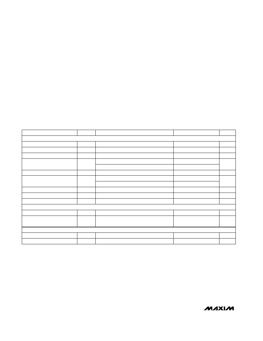
16-BIT DAC
16-BIT DATA LATCH
SERIAL INPUT REGISTER
CONTROL
LOGIC
MAX5541
REF
CS
DIN
SCLK
AGND
OUT
V
DD
DGND
Functional Diagram
19-1572; Rev 0; 12/99
PART
MAX5541CSA
MAX5541ESA
-40°C to +85°C
0°C to +70°C
TEMP. RANGE
PIN-PACKAGE
8 SO
8 SO
Ordering Information
SPI and QSPI are trademarks of Motorola, Inc.
MICROWIRE is a trademark of National Semiconductor Corp.
For free samples & the latest literature: http://www.maxim-ic.com, or phone 1-800-998-8800.
For small orders, phone 1-800-835-8769.
MAX5541
Low-Cost, +5V, Serial-Input,
Voltage-Output, 16-Bit DAC
2
_______________________________________________________________________________________
ABSOLUTE MAXIMUM RATINGS
ELECTRICAL CHARACTERISTICS
(V
DD
= +5V ±5%, V
REF
= +2.5V, V
AGND
= V
DGND
= 0, T
A
= T
MIN
to T
MAX
, unless otherwise noted. Typical values are at T
A
= +25°C.)
Stresses beyond those listed under "Absolute Maximum Ratings" may cause permanent damage to the device. These are stress ratings only, and functional
operation of the device at these or any other conditions beyond those indicated in the operational sections of the specifications is not implied. Exposure to
absolute maximum rating conditions for extended periods may affect device reliability.
V
DD
to DGND............................................................-0.3V to +6V
CS, SCLK, DIN to DGND..........................................-0.3V to +6V
REF to AGND, DGND ..................................-0.3V to (V
DD
+0.3V)
AGND to DGND.....................................................-0.3V to +0.3V
OUT to AGND, DGND.................................. ............-0.3V to V
DD
Maximum Current into Any Pin............................................50mA
Continuous Power Dissipation (T
A
= +70°C)
8-Pin SO (derate 5.88mW/°C above +70°C)................471mW
Operating Temperature Ranges
MAX5541CSA .....................................................0°C to +70°C
MAX5541ESA ..................................................-40°C to +85°C
Junction Temperature ......................................................+150°C
Storage Temperature Range .............................-65°C to +150°C
Lead Temperature (soldering, 10sec) ............................ +300°C
(Note 3)
4.75V
V
DD
5.25V
T
A
= T
MIN
to T
MAX
T
A
= +25°C
T
A
= T
MIN
to T
MAX
T
A
= +25°C
T
A
= T
MIN
to T
MAX
(Note 2)
CONDITIONS
k
11.5
R
REF
Reference Input Resistance
(Note 4)
V
2.0
3.0
V
REF
Reference Input Range
PSR
Power-Supply Rejection
LSB
±1.0
R
OUT
DAC Output Resistance
k
6.25
Bits
16
N
Resolution
ppm/°C
±0.1
Gain-Error Tempco
LSB
±10
Gain Error (Note 1)
±5
ppm/°C
±0.05
ZS
TC
Zero-Code Tempco
LSB
INL
Integral Nonlinearity
±4
±16
±1
±2
Zero-Code Offset Error
UNITS
MIN
TYP
MAX
SYMBOL
PARAMETER
ZSE
LSB
To ±
1
/
2
LSB of FS, C
L
= 10pF
1
µs
Output Settling Time
V
DD
= 5V
Guaranteed monotonic
Bits
±0.5
±1.0
DNL
Differential Nonlinearity
C
L
= 10pF (Note 5)
25
V/µs
SR
Voltage-Output Slew Rate
STATIC PERFORMANCE--ANALOG SECTION (R
L
=
)
REFERENCE INPUT
DYNAMIC PERFORMANCE--ANALOG SECTION (R
L
=
)
MAX5541
Low-Cost, +5V, Serial-Input,
Voltage-Output, 16-Bit DAC
_______________________________________________________________________________________
3
ELECTRICAL CHARACTERISTICS (continued)
(V
DD
= +5V ±5%, V
REF
= +2.5V, V
AGND
= V
DGND
= 0, T
A
= T
MIN
to T
MAX
, unless otherwise noted. Typical values are at T
A
= +25°C.)
TIMING CHARACTERISTICS
(V
DD
= +5V ±5%, V
REF
= +2.5V, V
AGND
= V
DGND
= 0, CMOS inputs, T
A
= T
MIN
to T
MAX
, unless otherwise noted.)
Note 1: Gain Error tested at V
REF
= +2.0V, +2.5V, and +3.0V.
Note 2: R
OUT
tolerance is typically ±20%.
Note 3: Min/Max ranges guaranteed by gain-error test. Operation outside min/max limits will result in degraded performance.
Note 4: Reference input resistance is code dependent, minimum at 8555 hex.
Note 5: Slew-rate value is measured from 0% to 63%.
Note 6: Guaranteed by design. Not production tested.
Code = 0000 hex, CS = V
DD
,
SCLK = V
DIN
= 0 to V
DD
levels
Major-carry transition
V
IN
= 0
Code = 0000 hex, V
REF
= 1Vp-p at 100kHz
Code = 0000 hex
Code = FFFF hex
(Note 6)
CONDITIONS
mW
1.5
PD
Power Dissipation
mA
0.3
1.1
I
DD
Positive Supply Current
V
4.75
5.25
V
DD
Positive Supply Range
V
0.40
V
H
Hysteresis Voltage
pF
10
C
IN
Input Capacitance
mVp-p
1
nVs
10
nVs
10
DAC Glitch Impulse
Digital Feedthrough
µA
±1
I
IN
Input Current
V
0.8
V
IL
Input Low Voltage
V
2.4
V
IH
Input High Voltage
Reference Feedthrough
dB
92
SNR
Signal-to-Noise Ratio
75
pF
120
C
IN
Reference Input Capacitance
UNITS
MIN
TYP
MAX
SYMBOL
PARAMETER
(Note 6)
CONDITIONS
µs
20
V
DD
High to CS Low
(power-up delay)
ns
45
t
CL
SCLK Pulse Width Low
ns
45
t
CH
MHz
10
f
CLK
SCLK Frequency
SCLK Pulse Width High
ns
0
t
DH
DIN to SCLK High Hold
ns
40
t
DS
DIN to SCLK High Setup
ns
45
t
CSS0
CS Low to SCLK High Setup
ns
45
t
CSS1
CS High to SCLK High Setup
ns
30
t
CSH0
SCLK High to CS Low Hold
ns
45
t
CSH1
SCLK High to CS High Hold
UNITS
MIN
TYP
MAX
SYMBOL
PARAMETER
Code = FFFF hex
MHz
1
BW
Reference -3dB Bandwidth
DYNAMIC PERFORMANCE--REFERENCE SECTION
STATIC PERFORMANCE--DIGITAL INPUTS
POWER SUPPLY
MAX5541
Low-Cost, +5V, Serial-Input,
Voltage-Output, 16-Bit DAC
4
_______________________________________________________________________________________
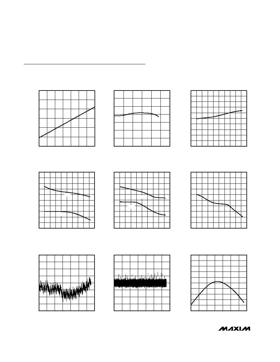
Typical Operating Characteristics
(V
DD
= +5V, V
REF
= +2.5V, T
A
= +25°C, unless otherwise noted.)
0.50
0.45
0.40
0.35
0.30
0.25
0.20
-40
-20
0
20
40
60
80
100
MAX5541-01
SUPPLY CURRENT (mA)
SUPPLY CURRENT
vs. TEMPERATURE
TEMPERATURE (°C)
0.35
0.34
0.33
0.32
0.31
0.30
0.29
0.28
0
1
2
3
4
5
6
MAX5541-02
SUPPLY CURRENT (mA)
SUPPLY CURRENT
vs. REFERENCE VOLTAGE
REFERENCE VOLTAGE (V)
1.0
0.6
0.2
0
-0.2
-0.6
0.8
0.4
-0.4
-0.8
-1.0
-60
-20
20
60
100
140
MAX5541-03
ZERO-CODE OFFSET ERROR (LSB)
ZERO-CODE OFFSET ERROR
vs. TEMPERATURE
TEMPERATURE (°C)
1.0
0.6
0.2
0
-0.2
-0.6
0.8
0.4
-0.4
-0.8
-1.0
-60
-20
20
60
100
140
MAX5541-04
INL (LSB)
INTEGRAL NONLINEARITY
vs. TEMPERATURE
TEMPERATURE (°C)
+INL
-INL
1.00
0.50
0.25
0.75
0
-0.25
-0.50
-0.75
-1.00
0
10k
20k
30k
40k
50k
60k
70k
MAX5541-07
INL (LSB)
INTEGRAL NONLINEARITY
vs. CODE
DAC CODE
1.0
0.6
0.2
0
-0.2
-0.6
0.8
0.4
-0.4
-0.8
-1.0
-60
-20
20
60
100
140
MAX5541-05
DNL (LSB)
DIFFERENTIAL NONLINEARITY
vs. TEMPERATURE
TEMPERATURE (°C)
+DNL
-DNL
1.0
0.8
0.6
0.4
0.2
0
-0.2
-0.4
-0.6
-0.8
-1.0
-60
-20
20
60
100
140
MAX5541-06
GAIN ERROR (LSB)
GAIN ERROR
vs. TEMPERATURE
TEMPERATURE (°C)
0.25
0.75
0.50
1.00
0
-0.25
-0.50
-0.75
-1.00
0
10k
20k
30k
40k
50k
60k
70k
MAX5541-08
DNL (LSB)
DIFFERENTIAL NONLINEARITY
vs. CODE
DAC CODE
200
160
120
80
40
0
0
10k
20k
30k
40k
50k
60k
70k
MAX5541-09
REFERENCE CURRENT (µA)
REFERENCE CURRENT
vs. CODE
DAC CODE
MAX5541
Low-Cost, +5V, Serial-Input,
Voltage-Output, 16-Bit DAC
_______________________________________________________________________________________
5
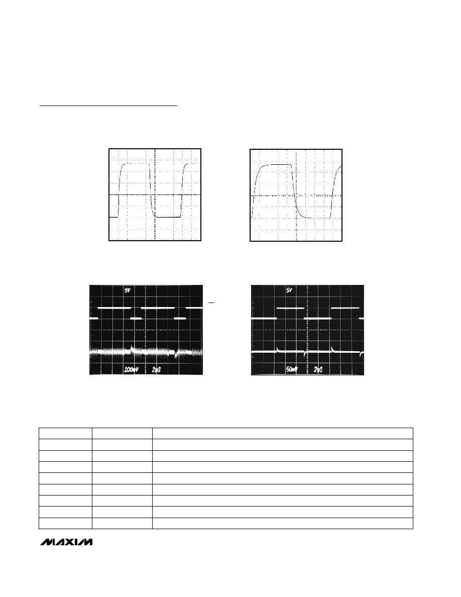
MAX5541-12
MAJOR-CARRY OUTPUT GLITCH
2
µs/div
CS
5V/div
OUT
AC-COUPLED
100mV/div
MAX5541-13
DIGITAL FEEDTHROUGH
2
µs/div
SCLK
5V/div
OUT
AC-COUPLED
50mV/div
CODE = 0000 hex
Typical Operating Characteristics (continued)
(V
DD
= +5V, V
REF
= +2.5V, T
A
= +25°C, unless otherwise noted.)
______________________________________________________________Pin Description
+5V Supply Voltage
V
DD
8
Digital Ground
DGND
7
Serial-Data Input
DIN
6
Serial-Clock Input. Duty cycle must be between 40% and 60%.
SCLK
5
Chip-Select Input
CS
4
Voltage Reference Input. Connect to external +2.5V reference.
REF
3
Analog Ground
AGND
2
DAC Output Voltage
OUT
1
FUNCTION
NAME
PIN
1
µs/div
FULL-SCALE STEP RESPONSE
(f
SCLK
= 10MHz)
MAX5541-10
OUT
500mV/div
C
L
= 13pF, R
L
=
400ns/div
FULL-SCALE STEP RESPONSE
(f
SCLK
= 20MHz)
MAX5541-11
OUT
500mV/div
C
L
= 13pF, R
L
=