 | –≠–ª–µ–∫—Ç—Ä–æ–Ω–Ω—ã–π –∫–æ–º–ø–æ–Ω–µ–Ω—Ç: MAX5547 | –°–∫–∞—á–∞—Ç—å:  PDF PDF  ZIP ZIP |

General Description
The MAX5547 dual, 10-bit, dual range, digital-to-analog
converter (DAC) sinks up to 3.6mA of current, making it
ideal for laser-driver-control applications. Parallel the
MAX5547 outputs to sink higher current (up to 7.2mA
max). Operating from a single +2.7V to +5.25V
supply, the MAX5547 typically consumes 1mA
(internal reference).
The MAX5547 operates from a precision +2.5V internal
4ppm/∞C reference or an external reference in the
+2.45V to +2.55V range. The maximum full-scale cur-
rent-sink range is software programmable to 3.6mA or
1.2mA for each DAC. A 10MHz SPITM-compatible serial
interface configures the device.
The MAX5547 is available in a 3mm x 3mm x 0.8mm 8-
pin TDFN package and is specified over the -40∞C to
+85∞C extended temperature range.
Applications
Laser-Driver Control
Pin-Diode Bias Currents
Modulation Currents
Average Power
Extinction Ratios
Features
Dual Current-Sink DACs
10-Bit Resolution
Two Software-Programmable Full-Scale Current
Ranges: 3.6mA or 1.2mA
Parallelable Outputs for Up to 7.2mA (max)
+2.5V Internal Reference Drifts Only 4ppm/∞C
+2.7V to +5.25V Single-Supply Operation
INL: ±4 LSB (1.2mA Output)
DNL: ±0.75 LSB (Guaranteed Monotonic)
Low +0.8V Output Compliance
Ultra-Small, 3mm x 3mm x 0.8mm, 8-Pin TDFN
Package
MAX5547
Dual, 10-Bit, Current-Sink Output DAC
________________________________________________________________ Maxim Integrated Products
1
19-3988; Rev 0; 2/06
For pricing, delivery, and ordering information, please contact Maxim/Dallas Direct! at
1-888-629-4642, or visit Maxim's website at www.maxim-ic.com.
Ordering Information
+2.7V TO +5.25V
+2.5V
+3.3V
OUTA
OUTB
CS
DIN
SCLK
MICROCONTROLLER WITH ADC
REF
I
I
BIASSET
MODSET
DIS
BC_MON
OUT-
OUT+
BIAS
AIN0
AIN1
AIN2
CS
MOSI
SCLK
GND
GND
V
CC
REF
FERRITE
BEAD
I/O1
I/O2
I/O3
TX_DISABLE
MOD-DEF1
MOD-DEF2
+3.3V
GND
V
CC
+3.3V
+3.3V
MAX5547
MAX3736
V
DD
Typical Operating Circuit
PART
TEMP RANGE
PIN-
PACKAGE
TOP
MARK
PKG
CODE
MAX5547ETA -40∞C to +85∞C 8 TDFN-EP*
APF
T833-2
SPI is a trademark of Motorola, Inc.
*EP = Exposed pad.
Pin Configuration appears at end of data sheet.

MAX5547
Dual, 10-Bit, Current-Sink Output DAC
2
_______________________________________________________________________________________
ABSOLUTE MAXIMUM RATINGS
Stresses beyond those listed under "Absolute Maximum Ratings" may cause permanent damage to the device. These are stress ratings only, and functional
operation of the device at these or any other conditions beyond those indicated in the operational sections of the specifications is not implied. Exposure to
absolute maximum rating conditions for extended periods may affect device reliability.
V
DD
to GND .............................................................-0.3V to +6V
OUTA, OUTB, REF to GND ........................-0.3V to (V
DD
+ 0.3V)
SCLK, DIN, CS to GND ............................................-0.3V to +6V
Continuous Power Dissipation (T
A
= +70∞C)
8-Pin TDFN (derate 18.2mW/∞C above +70∞C) .......1454.5mW
Operating Temperature Range ...........................-40∞C to +85∞C
Junction Temperature .....................................................+150∞C
Storage Temperature Range ............................-65∞C to +150∞C
Lead Temperature (soldering, 10s) ................................+300∞C
ELECTRICAL CHARACTERISTICS
(V
DD
= +2.7 to +5.25V, GND = 0, external reference = +2.5V, output voltage = +2.0V, T
A
= -40∞C to +85∞C. Typical values are at
V
DD
= +3.0V, and T
A
= +25∞C.) (Note 1)
PARAMETER
SYMBOL
CONDITIONS
MIN
TYP
MAX
UNITS
STATIC PERFORMANCE--ANALOG SECTION
Resolution
10
Bits
I
OUT
_ = 1.2mA
±4
Integral Nonlinearity (Note 2)
INL
I
OUT
_ = 3.6mA
±6
LSB
Differential Nonlinearity
DNL
Guaranteed monotonic
±0.75
LSB
Offset Error
OE
Code = 030h
±4
LSB
Offset Temperature Coefficent
0.05
LSB/∞C
I
OUT
= 1.2mA
±0.1
±3
Gain Error
GE
Measured from code
030h to 3FFh
I
OUT
= 3.6mA
±0.1
±5.5
%
I
OUT_
= 1.2mA
15
Gain Temperature Coefficient
I
OUT_
= 3.6mA
25
ppm/∞C
Line Regulation
V
DD
= +2.7V to +5.25V
0.8
LSB/V
Output Crosstalk
OUTA = midscale, OUTB switching from
030h to 3FFh
54
dB
REFERENCE
Internal-Reference Voltage
V
REF
T
A
= +25∞C
2.48
2.5
2.52
V
Internal-Reference Temperature
Coefficient
(Note 3)
4
35
ppm/∞C
Internal-Reference Load
Regulation
0µA < I
REF
< +300µA
1
3.5
Internal-Reference Power-Up
Time
C
REF
= 1µF, to 0.05%
0.55
ms
Internal-Reference Sink Current
50
µA
Internal-Reference Source
Current
300
µA
REF Capacitive Load
(Note 3)
0.1
10.0
µF
Reference Line Regulation
V
DD
= +2.7V to +5.25V
25
µV/V
f = 0.1Hz to 10Hz
10
Internal-Reference Noise
f = 10Hz to 10kHz
27
µV
RMS
External-Reference Range
V
REF
2.45
2.55
V

MAX5547
Dual, 10-Bit, Current-Sink Output DAC
_______________________________________________________________________________________
3
ELECTRICAL CHARACTERISTICS (continued)
(V
DD
= +2.7 to +5.25V, GND = 0, external reference = +2.5V, output voltage = +2.0V, T
A
= -40∞C to +85∞C. Typical values are at
V
DD
= +3.0V, and T
A
= +25∞C.) (Note 1)
PARAMETER
SYMBOL
CONDITIONS
MIN
TYP
MAX
UNITS
External-Reference Input
Impedance
R
REF
90
k
DAC OUTPUTS
Code = 030h
50
1.2mA low-current
range
Code = 3FFh
1170
1200
1230
Code = 030h
150
Output Current (Note 4)
I
OUT
_
3.6mA high-current
range
Code = 3FFh
3400
3600
3800
µA
1.2mA full-scale current
1.17
LSB Size
3.6mA full-scale current
3.52
µA
Current-Source Compliance
Voltage Range
I
OUT
_ = full-scale (Note 5)
0.8
V
DD
V
I
OUT
_ = 1.2mA
800
Output Impedance at Full-Scale
Current
I
OUT
_ = 3.6mA
180
k
DYNAMIC PERFORMANCE
Settling Time
t
S
To 1% (Note 6)
10
µs
f = 0.1Hz to 10Hz
0.05
Output Noise
I
RMS
f = 10Hz to 10kHz
0.35
LSB
RMS
Supply Feedthrough
100mV, 1kHz signal added to V
DD
0.85
LSB/V
Digital Feedthrough
R
LOAD
= 500
, C
LOAD
= 100pF
2
pA
∑
s
Digital-to-Analog Glitch Impulse
R
LOAD
= 500
, C
LOAD
= 100pF
16
pA
∑
s
DAC-to-DAC Full-Scale Current
Matching
2
%
POWER SUPPLIES
Supply Voltage
V
DD
+2.70
+5.25
V
Internal reference
mode
1.1
2
Supply Current
I
DD
V
DD
= +5.25V, no load,
SCLK not switching
External reference
mode
0.75
1.5
mA
LOGIC AND CONTROL INPUTS
Input High Voltage
V
IH
(Note 7)
0.7 x
V
DD
V
Input Low Voltage
V
IL
(Note 7)
0.8
V
Input Hysteresis
V
HYS
0.05 x
V
DD
V
Input Capacitance
C
IN
10
pF
Input Leakage Current
I
IN
±1
µA

MAX5547
Dual, 10-Bit, Current-Sink Output DAC
4
_______________________________________________________________________________________
ELECTRICAL CHARACTERISTICS (continued)
(V
DD
= +2.7 to +5.25V, GND = 0, external reference = +2.5V, output voltage = +2.0V, T
A
= -40∞C to +85∞C. Typical values are at
V
DD
= +3.0V, and T
A
= +25∞C.) (Note 1)
PARAMETER
SYMBOL
CONDITIONS
MIN
TYP
MAX
UNITS
SPI TIMING CHARACTERISTICS (see Figure 1)
SCLK Clock Period
t
CP
100
ns
SCLK Pulse-Width High
t
CH
40
ns
SCLK Pulse-Width Low
t
CL
40
ns
CS Fall to SCLK Fall Setup Time
t
CSS
25
ns
SCLK Fall to CS Rise Hold Time
t
CSH
50
ns
DIN to SCLK Fall Setup Time
t
DS
40
ns
DIN to SCLK Fall Hold Time
t
DH
0
ns
CS Pulse-Width High
t
CSW
100
ns
Note 1: Devices are 100% production tested at T
A
= +25∞C. Limits over temperature are guaranteed by design.
Note 2: INL linearity is from code 48 to code 1023.
Note 3: Guaranteed by design. Not production tested.
Note 4: The DACs continue to operate at currents lower than 50µA on the 1.2mA range and 150µA on the 3.6mA range. However,
performance is not guaranteed at these low currents. A code of all zeros has a nominal output current of 0µA.
Note 5: Compliance voltage range is defined as the range where the output current is -2 LSB of its value at V
OUT
= +1V.
Note 6: Settling time is measured from 0.25 x full scale to 0.75 x full scale.
Note 7: The device draws higher supply current when the digital inputs are driven with voltages between (V
DD
- 0.5V) and (GND +
0.5V). See Supply Current vs. Digital Input Voltage in the Typical Operating Characteristics.
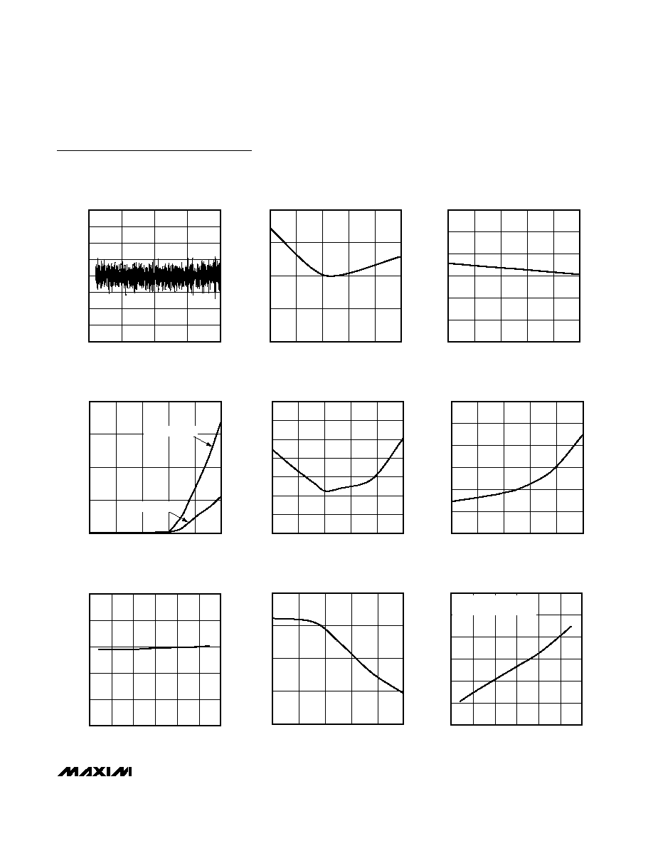
Typical Operating Characteristics
(V
DD
= +3.0V, GND = 0, external reference = +2.5V, T
A
= +25∞C, unless otherwise noted.)
-4
-3
-2
-1
0
1
2
3
4
0
256
512
768
1024
INTEGRAL NONLINEARITY
vs. DIGITAL INPUT CODE (1.2mA SETTING)
MAX5547 toc01
DIGITAL INPUT CODE
INL (LSB)
-4
-3
-2
-1
0
1
2
3
4
0
256
512
768
1024
INTEGRAL NONLINEARITY
vs. DIGITAL INPUT CODE (3.6mA SETTING)
MAX5547 toc02
DIGITAL INPUT CODE
INL (LSB)
-1.00
-0.75
-0.50
-0.25
0
0.25
0.50
0.75
1.00
0
256
512
768
1024
DIFFERENTIAL NONLINEARITY
vs. DIGITAL INPUT CODE (1.2mA SETTING)
MAX5547 toc03
DIGITAL INPUT CODE
DNL (LSB)
MAX5547
Dual, 10-Bit, Current-Sink Output DAC
_______________________________________________________________________________________
5
Typical Operating Characteristics (continued)
(V
DD
= +3.0V, GND = 0, external reference = +2.5V, T
A
= +25∞C, unless otherwise noted.)
-1.00
-0.75
-0.50
-0.25
0
0.25
0.50
0.75
1.00
0
256
512
768
1024
DIFFERENTIAL NONLINEARITY
vs. DIGITAL INPUT CODE (3.6mA SETTING)
MAX5547 toc04
DIGITAL INPUT CODE
DNL (LSB)
8
6
4
2
0
-40
10
-15
35
60
85
MAXIMUM INTEGRAL NONLINEARITY
vs. TEMPERATURE (3.6mA SETTING)
MAX5547 toc05
TEMPERATURE (
∞C)
INL (LSB)
0
0.2
0.1
0.4
0.3
0.5
0.6
-40
85
MAXIMUM DIFFERENTIAL NONLINEARITY
vs. TEMPERATURE (3.6mA SETTING)
MAX5547 toc06
TEMPERATURE (
∞C)
DNL (LSB)
10
-15
35
60
20
15
10
5
0
-40
10
-15
35
60
85
ZERO-SCALE SINK CURRENT
vs. TEMPERATURE
MAX5547 toc07
TEMPERATURE (
∞C)
ZERO-SCALE CURRENT (
µ
A)
3.6mA FULL SCALE
1.2mA FULL SCALE
1.196
1.200
1.198
1.204
1.202
1.208
1.206
1.210
-40
10
-15
35
60
85
FULL-SCALE SINK CURRENT
vs. TEMPERATURE (1.2mA SETTING)
MAX5547 toc08
TEMPERATURE (
∞C)
FULL-SCALE CURRENT (mA)
3.50
3.60
3.55
3.70
3.65
3.75
3.80
-40
10
-15
35
60
85
FULL-SCALE SINK CURRENT
vs. TEMPERATURE (3.6mA SETTING)
MAX5547 toc09
TEMPERATURE (
∞C)
FULL-SCALE CURRENT (mA)
2.4950
2.4952
2.4956
2.4954
2.4958
2.4960
2.5
3.5
3.0
4.0
4.5
5.0
5.5
INTERNAL REFERENCE VOLTAGE
vs. SUPPLY VOLTAGE
MAX5547 toc10
SUPPLY VOLTAGE (V)
INTERNAL REFERENCE VOLTAGE (V)
2.4940
2.4935
2.4930
2.4925
2.4920
-40
10
-15
35
60
85
INTERNAL REFERENCE
VOLTAGE vs. TEMPERATURE
MAX5547 toc11
TEMPERATURE (
∞C)
INTERNAL REFERENCE VOLTAGE (V)
490
494
492
498
496
500
502
2.5
3.5
4.0
3.0
4.5
5.0
5.5
SUPPLY CURRENT vs. SUPPLY VOLTAGE
MAX5547 toc12
SUPPLY VOLTAGE (V)
I
DD
(
µ
A)
EXTERNAL REFERENCE = 2.5V,
CS = SCLK = DIN = GND