 | –≠–ª–µ–∫—Ç—Ä–æ–Ω–Ω—ã–π –∫–æ–º–ø–æ–Ω–µ–Ω—Ç: MAX5632 | –°–∫–∞—á–∞—Ç—å:  PDF PDF  ZIP ZIP |
For pricing, delivery, and ordering information, please contact Maxim/Dallas Direct! at
1-888-629-4642, or visit Maxim's website at www.maxim-ic.com.
General Description
The MAX5631/MAX5632/MAX5633 are 16-bit digital-to-
analog converters (DACs) with 32 sample-and-hold
(SHA) outputs for applications where a high number of
programmable voltages are required. These devices
include a clock oscillator and a sequencer that updates
the DAC with codes from an internal SRAM. No external
components are required to set offset and gain.
The MAX5631/MAX5632/MAX5633 feature a -4.5V to
+9.2V output voltage range. Other features include a
200µV/step resolution, with output linearity error, typi-
cally 0.005% of full-scale range (FSR). The 100kHz
refresh-rate updates each SHA every 320µs, resulting
in negligible output droop. Remote ground sensing
allows the outputs to be referenced to the local ground
of a separate device.
These devices are controlled through a 20MHz
SPITM/QSPITM/MICROWIRETM-compatible 3-wire serial
interface. Immediate Update Mode allows any chan-
nel's output to be updated within 20µs. Burst Mode
allows multiple values to be loaded into memory in a
single, high-speed data burst. All channels are updated
within 330µs after data has been loaded.
Each device features an output clamp and output resis-
tors for filtering. The MAX5631 features a 50
output
impedance and is capable of driving up to 250pF of out-
put capacitance. The MAX5632 features a 500
output
impedance and is capable of driving up to 10nF of output
capacitance. The MAX5633 features a 1k
output imped-
ance and is capable of driving up to 10nF of output
capacitance.
The MAX5631/MAX5632/MAX5633 are available in 12mm
x 12mm, 64-pin TQFP, and 10mm x 10mm, 68-pin thin
QFN packages.
________________________Applications
MEMS Mirror Servo Control
Industrial Process Control
Automatic Test Equipment
Instrumentation
Features
o Integrated 16-Bit DAC and 32-Channel SHA with
SRAM and Sequencer
o 32 Voltage Outputs
o 0.005% Output Linearity
o 200µV Output Resolution
o Flexible Output Voltage Range
o Remote Ground Sensing
o Fast Sequential Loading: 1.3µs per Register
o Burst and Immediate Mode Addressing
o No External Components Required for Setting
Gain and Offset
o Integrated Output Clamp Diodes
o Three Output Impedance Options:
MAX5631 (50
), MAX5632 (500), and
MAX5633 (1k
)
19-2171; Rev 3; 1/05
MAX5631/MAX5632/MAX5633
16-Bit DACs with 32-Channel
Sample-and-Hold Outputs
________________________________________________________________ Maxim Integrated Products
1
Pin Configurations
Ordering Information
*For other temperature-range options, contact factory.
SPI and QSPI are trademarks of Motorola, Inc.
MICROWIRE is a trademark of National Semiconductor, Corp.
PART
TEMP RANGE*
PIN-PACKAGE
MAX5631UCB
0∞C to +85∞C
64 TQFP
MAX5631UTK
0∞C to +85∞C
68 Thin QFN
MAX5632UCB
0∞C to +85∞C
64 TQFP
MAX5632UTK
0∞C to +85∞C
68 Thin QFN
MAX5633UCB
0∞C to +85∞C
64 TQFP
MAX5633UTK
0∞C to +85∞C
68 Thin QFN
Pin Configurations continued at end of data sheet.
58
59
60
61
62
54
55
56
57
63
38
39
40
41
42
43
44
45
46
47
ECLK
OUT0
V
REF
TQFP
TOP VIEW
AGND
OUT31
OUT30
OUT29
OUT28
OUT27
OUT26
AGND
OUT25
52
53
49
50
51
OUT24
OUT23
OUT22
OUT21
CL
CL
OUT2
OUT1
OUT4
OUT3
AGND
OUT5
OUT7
OUT6
OUT9
OUT8
CH
OUT10
V
SS
CH
V
SS
OUT20
OUT19
OUT18
OUT17
OUT16
AGND
V
DD
OUT15
33
34
35
36
37
OUT14
OUT13
OUT12
OUT11
CL
IMMED
V
LOGIC
SCLK
DIN
CS
V
SS
AGND
V
LSHA
DGND
CLKSEL
RST
V
LDAC
GS
N.C.
48
V
DD
N.C.
64
CH
V
DD
23
22
21
20
19
27
26
25
24
18
29
28
32
31
30
17
11
10
9
8
7
6
5
4
3
2
16
15
14
13
12
1
MAX5631
MAX5632
MAX5633
MAX5631/MAX5632/MAX5633
16-Bit DACs with 32-Channel
Sample-and-Hold Outputs
2
_______________________________________________________________________________________
ABSOLUTE MAXIMUM RATINGS
ELECTRICAL CHARACTERISTICS
(V
DD
= +10V, V
SS
= -4V, V
LOGIC
= V
LDAC
= V
LSHA
= +5V, V
REF
= +2.5V, AGND = DGND = V
GS
= 0, R
L
10M, C
L
= 50pF,
CLKSEL = +5V, f
ECLK
= 400kHz, T
A
= T
MIN
to T
MAX
, unless otherwise noted. Typical values are at T
A
= +25∞C.)
Stresses beyond those listed under "Absolute Maximum Ratings" may cause permanent damage to the device. These are stress ratings only, and functional
operation of the device at these or any other conditions beyond those indicated in the operational sections of the specifications is not implied. Exposure to
absolute maximum rating conditions for extended periods may affect device reliability.
V
DD
to AGND.......................................................-0.3V to +12.2V
V
SS
to AGND .........................................................-6.0V to +0.3V
V
DD
to V
SS
...........................................................................+15V
V
LDAC
, V
LOGIC
, V
LSHA
to AGND or DGND ..............-0.3V to +6V
REF to AGND............................................................-0.3V to +6V
GS to AGND................................................................V
SS
to V
DD
CL and CH to AGND...................................................V
SS
to V
DD
Logic Inputs to DGND ..............................................-0.3V to +6V
DGND to AGND........................................................-0.3V to +2V
Maximum Current Into OUT_ ............................................±10mA
Maximum Current Into Logic Inputs .................................±20mA
Continuous Power Dissipation (T
A
= +70∞C)
64-Pin TQFP (derate 13.3mW/∞C above +70∞C) ............1066mW
68-Pin QFN (derate 28.6mW/∞C above +70∞C) ..............2285mW
Operating Temperature Range...............................0∞C to +85∞C
Maximum Junction Temperature .....................................+150∞C
Storage Temperature Range .............................-65∞C to +150∞C
Lead Temperature (soldering, 10s) .................................+300∞C
PARAMETER
SYMBOL
CONDITIONS
MIN
TYP
MAX
UNITS
DC CHARACTERISTICS
Resolution
N
16
Bits
Output Range
V
OUT_
(Note 1)
V
SS
+
0.75
V
DD
-
2.4
V
Offset Voltage
Code = 4F2C hex
±15
±200
mV
Offset Voltage Tempco
±50
µV/∞C
Gain Error
(Note 2)
±1
%
Gain Tempco
±5
ppm/∞C
Integral Linearity Error
INL
V
OUT_
= -3.25V to +7.6V
0.005
0.015
%FSR
Differential Linearity Error
DNL
V
OUT_
= -3.25V to +7.6V. Monotonicity
guaranteed to 14 bits
±1
±4
LSB
Maximum Output Drive Current
I
OUT
Sinking and sourcing
±2
mA
MAX5631
35
50
65
MAX5632
350
500
650
DC Output Impedance
R
OUT
MAX5633
700
1000
1300
MAX5631
250
pF
MAX5632
10
Maximum Capacitive Load
MAX5633
10
nF
DC Crosstalk
Internal oscillator enabled (Note 3)
-90
dB
Power-Supply Rejection Ratio
PSRR
Internal oscillator enabled
-80
dB
MAX5631/MAX5632/MAX5633
16-Bit DACs with 32-Channel
Sample-and-Hold Outputs
_______________________________________________________________________________________
3
ELECTRICAL CHARACTERISTICS (continued)
(V
DD
= +10V, V
SS
= -4V, V
LOGIC
= V
LDAC
= V
LSHA
= +5V, V
REF
= +2.5V, AGND = DGND = V
GS
= 0, R
L
10M, C
L
= 50pF,
CLKSEL = +5V, f
ECLK
= 400kHz, T
A
= T
MIN
to T
MAX
, unless otherwise noted. Typical values are at T
A
= +25∞C.)
PARAMETER
SYMBOL
CONDITIONS
MIN
TYP
MAX
UNITS
DYNAMIC CHARACTERISTICS
Sample-and-Hold Settling
(Notes 4)
0.08
%
SCLK Feedthrough
0.5
nV-s
f
SEQ
Feedthrough
0.5
nV-s
Hold-Step
0.25
1
mV
Droop Rate
V
OUT
_
= 0 (Note 5), T
A
= +25∞C
1
40
mV/s
Output Noise
250
µV
RMS
REFERENCE INPUT
Input Resistance
7
k
Reference Input Voltage
V
REF
2.5
V
GROUND SENSE INPUT
Input Voltage Range
V
GS
-0.5
0.5
V
Input Bias Current
I
GS
-0.5
V
GS
0.5
-60
0
µA
GS Gain
(Note 6)
0.998
1
1.002
V/V
DIGITAL INTERFACE DC CHARACTERISTICS
Input High Voltage
V
IH
2.0
V
Input Low Voltage
V
IL
0.8
V
Input Current
±1
µA
TIMING CHARACTERISTICS (FIGURE 2)
Sequencer Clock Frequency
f
SEQ
Internal oscillator
80
100
120
kHz
External Clock Frequency
f
ECLK
(Note 7)
440
kHz
SCLK Frequency
f
SCLK
20
MHz
SCLK Pulse Width High
t
CH
15
ns
SCLK Pulse Width Low
t
CL
15
ns
CS Low to SCLK High Setup
Time
t
CSSO
15
ns
CS High to SCLK High Setup
Time
t
CSS1
15
ns
SCLK High to
CS Low Hold Time
t
CSH0
10
ns
MAX5631/MAX5632/MAX5633
16-Bit DACs with 32-Channel
Sample-and-Hold Outputs
4
_______________________________________________________________________________________
Note 1: The nominal zero-scale (code = 0) voltage is -4.0535V. The nominal full-scale (code = FFFF hex) voltage is +9.0535V. The
output voltage is limited by the Output Range specification, restricting the useable range of DAC codes. The nominal zero-
scale voltage may be achieved when V
SS
< -4.9V, and the nominal full-scale voltage may be achieved when V
DD
> +11.5V.
Note 2: Gain is calculated from measurements
for voltages V
DD
= 10V and V
SS
= -4V at codes C000 hex and 4F2C hex,
for voltages V
DD
= 11.6V and V
SS
= -2.9V at codes FFFF hex and 252E hex,
for voltages V
DD
= 9.25V and V
SS
= -5.25V at codes D4F6 hex and 0 hex, and
for voltages V
DD
= 8.55V and V
SS
= -2.75V at codes C74A hex and 281C hex.
Note 3: Steady-state change in any output with an 8V change in an adjacent output.
Note 4: Settling during the first update for an 8V step. The output will settle to within the linearity specification on subsequent
updates. Tested with an external sequencer clock frequency of 480kHz.
Note 5: External clock mode with the external clock not toggling.
Note 6: The output voltage is the sum of the DAC output and the voltage at GS. GS gain is measured at 4F2C hex.
Note 7: The sequencer runs at f
SEQ
= f
ECLK
/4. Maximum speed is limited by settling of the DAC and SHAs. Minimum speed is
limited by acceptable droop and update time after a Burst Mode Update.
Note 8: V
DD
rise to
CS low = 500µs maximum.
Note 9: Guaranteed by gain-error test.
Note 10: The serial interface is inactive. V
IH
= V
LOGIC
, V
IL
= 0.
Note 11: The serial interface is active. V
IH
= V
LOGIC
, V
IL
= 0.
ELECTRICAL CHARACTERISTICS (continued)
(V
DD
= +10V, V
SS
= -4V, V
LOGIC
= V
LDAC
= V
LSHA
= +5V, V
REF
= +2.5V, AGND = DGND = V
GS
= 0, R
L
10M, C
L
= 50pF,
CLKSEL = +5V, f
ECLK
= 400kHz, T
A
= T
MIN
to T
MAX
, unless otherwise noted. Typical values are at T
A
= +25∞C.)
PARAMETER
SYMBOL
CONDITIONS
MIN
TYP
MAX
UNITS
SCLK High to
CS High Hold Time
t
CSH1
0
ns
DIN to SCLK High Setup Time
t
DS
15
ns
DIN to SCLK High Hold Time
t
DH
0
ns
RST to CS Low
(Note 8)
500
µs
POWER SUPPLIES
Positive Supply Voltage
V
DD
(Note 9)
8.55
10
11.6
V
Negative Supply Voltage
V
SS
(Note 9)
-5.25
-4
-2.75
V
Supply Difference
V
DD
- V
SS
(Note 9)
14.5
V
Logic Supply Voltage
V
LOGIC
,
V
LDAC
,
V
LSHA
4.75
5
5.25
V
Positive Supply Current
I
DD
32
42
mA
Negative Supply Current
I
SS
32
40
mA
(Note 10)
1
1.5
Logic Supply Current
I
LOGIC
f
SCLK
= 20MHz (Note 11)
2
3
mA
-0.007
-0.003
-0.005
0.001
-0.001
0.005
0.003
0.007
4018
19520 27271
11769
35021 42723 58268
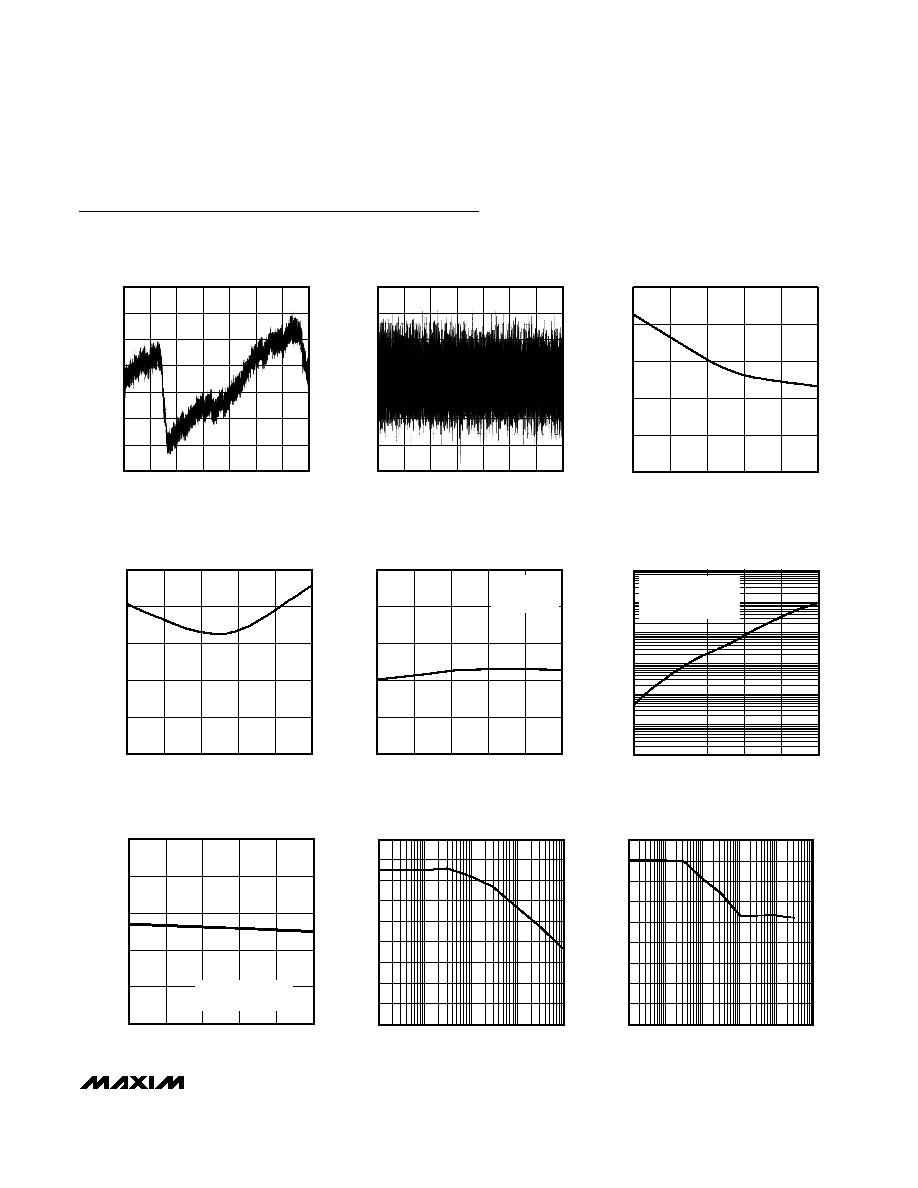
INTEGRAL NONLINEARITY vs. CODE
MAX5631 toc01
INPUT CODE
INTEGRAL NONLINEARITY (%)
-1.4
-0.6
-1.0
0.2
-0.2
1.0
0.6
1.4
DIFFERENTIAL NONLINEARITY vs. CODE
MAX5631 toc02
INPUT CODE
DIFFERENTIAL NONLINEARITY (LSB)
4018
19520 27271
11769
35021 42723 58268
0
0.002
0.006
0.004
0.008
0.010
-40
10
-15
35
60
85
INTEGRAL NONLINEARITY
VS.
TEMPERATURE
MAX5631 toc03
TEMPERATURE (
∞C)
INTEGRAL NONLINEARITY (%)
0.5
0.6
0.8
0.7
0.9
1.0
-40
10
-15
35
60
85
DIFFERENTIAL NONLINEARITY
VS.
TEMPERATURE
MAX5631 toc04
TEMPERATURE (
∞C)
DIFFERENTIAL NONLINEARITY (LSB)
-20
-18
-14
-16
-12
-10
-40
10
-15
35
60
85
OFFSET VOLTAGE
VS.
TEMPERATURE
MAX5631 toc05
TEMPERATURE (
∞C)
OFFSET VOLTAGE (mV)
V
DD
= +8.55V
V
SS
= -4V
CODE = 4F2C hex
DROOP RATE vs. TEMPERATURE
TEMPERATURE (
∞C)
-40
35
60
-15
10
85
DROOP RATE (mV/s)
100
0.0001
0.001
0.010
0.100
10
1
MAX5631 toc06
CODE = 4F2C hex
EXTERNAL CLOCK MODE
NO CLOCK APPLIED
0
0.01
0.03
0.02
0.04
0.05
-40
10
-15
35
60
85
GAIN ERROR
VS.
TEMPERATURE
MAX5631 toc07
TEMPERATURE (
∞C)
GAIN ERROR (%)
CODE = C168 hex
OFFSET CODE = 4F2C hex
10
100
0
-10
-20
-30
-40
-60
-50
-70
-80
0.01
0.1
1
POSITIVE SUPPLY PSRR
VS.
FREQUENCY
MAX5361 toc08
FREQUENCY (kHz)
PSRR (dB)
-90
-90
0
0.001
0.01
0.1
1
10
100
NEGATIVE SUPPLY PSRR
VS.
FREQUENCY
-10
-20
MAX5631 toc09
FREQUENCY (kHz)
PSRR (dB)
-40
-30
-70
-80
-60
-50
Typical Operating Characteristics
(V
DD
= +10V, V
SS
= -4V, V
REF
= +2.5V, V
GS
= 0, T
A
= +25∞C, unless otherwise noted.)
MAX5631/MAX5632/MAX5633
16-Bit DACs with 32-Channel
Sample-and-Hold Outputs
_______________________________________________________________________________________
5